EP1868223A2 - Anzeigetafel - Google Patents
Anzeigetafel Download PDFInfo
- Publication number
- EP1868223A2 EP1868223A2 EP07102390A EP07102390A EP1868223A2 EP 1868223 A2 EP1868223 A2 EP 1868223A2 EP 07102390 A EP07102390 A EP 07102390A EP 07102390 A EP07102390 A EP 07102390A EP 1868223 A2 EP1868223 A2 EP 1868223A2
- Authority
- EP
- European Patent Office
- Prior art keywords
- light
- display panel
- light guides
- filter
- disposed
- Prior art date
- Legal status (The legal status is an assumption and is not a legal conclusion. Google has not performed a legal analysis and makes no representation as to the accuracy of the status listed.)
- Granted
Links
Images


Classifications
-
- H—ELECTRICITY
- H01—ELECTRIC ELEMENTS
- H01J—ELECTRIC DISCHARGE TUBES OR DISCHARGE LAMPS
- H01J11/00—Gas-filled discharge tubes with alternating current induction of the discharge, e.g. alternating current plasma display panels [AC-PDP]; Gas-filled discharge tubes without any main electrode inside the vessel; Gas-filled discharge tubes with at least one main electrode outside the vessel
- H01J11/10—AC-PDPs with at least one main electrode being out of contact with the plasma
- H01J11/12—AC-PDPs with at least one main electrode being out of contact with the plasma with main electrodes provided on both sides of the discharge space
-
- H—ELECTRICITY
- H01—ELECTRIC ELEMENTS
- H01J—ELECTRIC DISCHARGE TUBES OR DISCHARGE LAMPS
- H01J11/00—Gas-filled discharge tubes with alternating current induction of the discharge, e.g. alternating current plasma display panels [AC-PDP]; Gas-filled discharge tubes without any main electrode inside the vessel; Gas-filled discharge tubes with at least one main electrode outside the vessel
- H01J11/20—Constructional details
- H01J11/34—Vessels, containers or parts thereof, e.g. substrates
- H01J11/44—Optical arrangements or shielding arrangements, e.g. filters, black matrices, light reflecting means or electromagnetic shielding means
-
- H—ELECTRICITY
- H01—ELECTRIC ELEMENTS
- H01J—ELECTRIC DISCHARGE TUBES OR DISCHARGE LAMPS
- H01J2211/00—Plasma display panels with alternate current induction of the discharge, e.g. AC-PDPs
- H01J2211/20—Constructional details
- H01J2211/34—Vessels, containers or parts thereof, e.g. substrates
- H01J2211/44—Optical arrangements or shielding arrangements, e.g. filters or lenses
- H01J2211/444—Means for improving contrast or colour purity, e.g. black matrix or light shielding means
Definitions
- the present invention relates to a display panel, and more particularly, to an advanced display panel which displays images using a plasma type of display.
- PDP plasma display panels
- display images using electric discharge are widely popular due to their display performance, including superior luminance, visual angle and other features.
- PDPs are divided into a facing discharge type and a surface discharge type, depending on the location structure of the electrodes.
- Facing discharge type PDPs have a pair of sustaining electrodes which is disposed on an upper substrate and a lower substrate, and form an electric discharge in a direction perpendicular to the panel.
- Surface discharge type PDPs have a pair of sustaining electrodes which is disposed on the same substrate, and generates an electric discharge on one surface.
- Facing discharge type PDPs have a high luminous efficacy, but suffer from the problem that phosphor is easily degraded by the electric discharge, thus, recently surface discharge type PDPs have become more widely used.
- Figure 1 shows the structure of a conventional PDP.
- the PDP in Figure 1 is a surface discharge type PDP.
- the PDP is partially incised and an upper substrate 20 is rotated at a 90° angle.
- a plurality of address electrodes 11 are disposed on the lower substrate 10 in a striped pattern and are buried by a first dielectric layer 12, which is white.
- a plurality of dams 13 are formed on the first dielectric layer 12 at predetermined intervals in order to prevent electrical and optical cross-talk between discharge cells 15.
- the insides of the discharge cells 15, which are partitioned by the plurality of dams 13, are coated with a phosphor layer 14 and are filled with discharge gas for plasma discharge.
- the discharge gas is a mixture of neon (Ne), Xenon (Xe) and other gases.
- the upper substrate 20 is a transparent substrate through which visible light can penetrate, is made mainly of glass, and is sealed on the lower substrate 10 with the dams 13.
- Sustaining electrodes 21a and 21b are disposed in pairs under the upper substrate 20 and are perpendicular to the address electrodes 11.
- the sustaining electrodes 21a and 21b are made of transparent conductive material such as Indium Tin Oxide (ITO).
- ITO Indium Tin Oxide
- bus electrodes 22a and 22b composed of metal are disposed under the sustaining electrodes 21a and 21b and have a narrower width than the sustaining electrodes 21a and 21b.
- the sustaining electrodes 21a and 21b and the bus electrodes 22a and 22b are buried by a second dielectric layer 23, which is transparent.
- a protection layer 24 is disposed under the second dielectric layer 23.
- the protection layer 24 prevents damage to the second dielectric layer 23 caused by sputtering of plasma particles, emits secondary electrons so as to lower discharge voltage and sustaining voltage, and is generally composed of magnesium oxide (MgO).
- a plurality of black stripes 30 are disposed on the upper substrate 20 at predetermined intervals parallel to the sustaining electrodes 21a and 21b so as to prevent external light from entering the inside of the panel.
- a wall charge is formed by generating an address discharge between one of the sustaining electrodes 21a and 21b and the address electrode 11, and then sustaining discharge is generated by the electric potential difference between the pair of sustaining electrodes 21a and 21b, so ultraviolet rays are generated by the discharge gas.
- the phosphor layer 14 is excited by the ultraviolet rays, causing visible light to be emitted.
- the visible light exits the upper substrate 20 and forms images which are perceptible to the user.
- Exemplary embodiments of the present invention address at least some of the above problems and/or disadvantages.
- An apparatus consistent with the present invention provides a PDP having an upper substrate of an improved structure so as to enhance the bright room contrast of the PDP.
- Another apparatus consistent with the present invention provides a PDP employing a filter with an improved structure so as to enhance the bright room contrast of the PDP.
- an exemplary display panel comprising: a plurality of light guides which emit received light; and a plurality of external light blocking members which are disposed between exit surfaces of the plurality of light guides, and block light from the outside.
- spaces are formed between the plurality of light guides.
- the spaces are formed under the plurality of external light blocking members.
- the space is filled with gaseous material.
- the external light blocking member is composed of carbon black of maximum density.
- the light guide has an exit surface which is wider than the incidence surface through which light enters.
- the display panel further comprises an electromagnetic interface (EMI) prevention layer which is formed as a mesh or as a conductive film and prevents EMI; an antireflection layer which is formed as an anti-reflective (AR) film and prevents external light from being reflected; and a near infrared blocking layer which blocks near infrared rays included in light rays passing through the light guide.
- EMI electromagnetic interface
- AR anti-reflective
- a plasma display panel comprising: a lower substrate and an upper substrate which are separated to form a plurality of discharge cells therebetween, wherein the upper substrate comprises a plurality of light guides which focus and emit light generated from the plurality of discharge cells; and a plurality of external light blocking members which are disposed between exit surfaces of the plurality of light guides, and block light from the outside.
- spaces are formed on the upper substrate by being surrounded by the plurality of light guides and the plurality of external light blocking members.
- the space is filled with gaseous material.
- the gaseous material is air.
- the PDP further comprises a plurality of address electrodes which are disposed on the lower substrate in a striped pattern and generate a wall charge in the discharge cells.
- the plurality of light guides are parallel to the plurality of address electrodes, or perpendicular to the plurality of address electrodes.
- a filter which filters screen output of a display device, the filter comprising: a plurality of light guides which emit received light; and a plurality of external light blocking members which are disposed between exit surfaces of the plurality of light guides, and block light from the outside.
- spaces may be formed between the plurality of light guides.
- the spaces are formed under the plurality of external light blocking members.
- the space is filled with gaseous material.
- the gaseous material is air.
- the external light blocking member may be composed of carbon black of maximum density.
- the light guide has an exit surface wider than the incidence surface through which light enters.
- the display device is a PDP.
- a filter comprising: a plurality of light guides which are bonded on a display panel, and focus, and emit light generated from the display panel; and a plurality of external light blocking members which are disposed between exit surfaces of the plurality of light guides, and block light from the outside, wherein air layers are formed between the plurality of light guides and the plurality of external light blocking members.
- Figure 2 shows the structure of a PDP according to an exemplary embodiment of the present invention.
- the plasma display panel (PDP) in Figure 2 according to an exemplary embodiment of the present invention comprises an upper substrate 130 and a lower substrate 110 which are separated from each other.
- a plurality of discharge cells 115 are formed between the upper substrate 130 and the lower substrate 110 and cause plasma discharge.
- the lower substrate 110 is a glass substrate and has a plurality of address electrodes 111 arranged in a striped pattern thereon for address discharge.
- a first dielectric layer 112 is disposed on the lower substrate 110 to cover the address electrodes 111 and is formed by applying a predetermined thickness of dielectric material, which is white, on the lower substrate 110.
- a plurality of dams 113 are disposed on the first dielectric layer 112 at predetermined intervals parallel to the address electrodes 111.
- the plurality of dams 113 form discharge cells 115 by partitioning space between the lower substrate 110 and the upper substrate 130, and prevent electrical and optical cross-talk between discharge cells 115 to enhance color purity.
- a phosphor layer 114 of red, green and blue colors is applied on the first dielectric layer 112 and both sides of the dams 113, which constitute the inner wall of the discharge cell 115, at a predetermined thickness.
- the inside of the discharge cell 115 is filled with discharge gas which is a mixture of neon (Ne), generally used for plasma discharge, and a small amount of Xenon (Xe).
- the phosphor layer 114 is excited by ultraviolet rays generated by plasma discharge of the discharge gas, and emits visible light corresponding to the phosphor layer 114 of each color.
- the upper substrate 130 comprises light guides 131 which focus and emit ultraviolet rays generated by discharge.
- the light guides 131 are disposed parallel to the address electrodes 111.
- An external light blocking member 132 is disposed between exit surfaces 131b of the light guides 131 to block light from the outside to the discharge cell 115.
- a space 133 which is surrounded by the light guides 131 and the external light blocking member 132, is formed on the upper substrate 130 and is filled with gases such as air.
- the external light blocking member 132 is composed of carbon black of maximum density and absorbs light from the outside, so that it can prevent contrast from being lowered by external light.
- the external light blocking member 132 may comprise a conductive film (not shown) for blocking electro-magnetic interference (EMI).
- the light guides 131 can be configured so that one light guide 131 corresponds to one discharge cell 115 as shown in Figure 2, or can be configured so that one light guide 131 corresponds to several discharge cells 115.
- an incidence surface 131a thereof is wider than the exit surface 131b, so visible light generated from the discharge cell 115 is received through the incidence surface 131a and focused so as to exit through the exit surface 131b.
- the light guide 131 can be produced in a width of scores of ⁇ m, it can be used to implement high precision images to enhance the luminance of a panel. Moreover, the exit surfaces 131b of the light guides 131 are processed with non-glare treatment, so it can prevent glare caused by reflecting external light from the exit surface 131b of the light guide 131.
- a discharge electrode 121a is disposed under the upper substrate 130 for sustaining discharge and is perpendicular to the address electrode 111.
- the discharge electrodes 121a are disposed in pairs in the same manner as the electrodes in Figure 1, but the upper substrate 130 of Figure 2 is not rotated to 90°, so just one discharge electrode 121a is illustrated in Figure 2.
- the discharge electrode 121a is composed of mainly transparent conductive material such as indium tin oxide (ITO) so that visible light generated from the discharge cell 115 may pass through.
- a bus electrode 122a is disposed under the discharge electrode 121a and is composed of metal.
- the bus electrodes 122a are disposed in pairs in the same manner as the discharge electrodes 121a.
- the bus electrode 122a reduces line resistance of the discharge electrodes 121a and has a narrower width than the discharge electrodes 121a.
- a second dielectric layer 123 is disposed to cover the discharge electrodes 121a and the bus electrode 122a.
- the second dielectric layer 123 can be formed by applying a predetermined thickness of transparent dielectric material under the upper substrate 130.
- a protection layer 124 is disposed under the second dielectric layer 123, prevents damage of the second dielectric layer 123 and the discharge electrodes 121a caused by the sputtering of plasma particles, emits secondary electrons so as to lower discharge voltage.
- the protection layer 124 can be formed by applying a predetermined thickness of magnesium oxide (MgO) under the second dielectric layer 123.
- MgO magnesium oxide
- the visible light is received and focused by the incidence surface 131a of the light guide 131 and exits through the exit surface 131b. As the interface of the light guide 131 is processed not to cause light scattering, total reflection inside the light guide 131 is maximized. At this time, the external light blocking member 132 prevents external light from entering the discharge cell 115 or reflecting, so that the bright room contrast is enhanced.
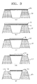
- Figures 3(a) - 3(b) are drawings describing a process of forming an external light blocking member of a PDP according to an exemplary embodiment of the present invention.
- the area of the exit surface 131b in Figure 3 is smaller than that of the incidence surface 131a, a bonding agent (not shown) is applied to the exit surface 131b, and the external light blocking member 132 is attached thereto ( Figure 3(a)).
- the external light blocking member 132 is made of carbon black of maximum density.
- a photosensitive material 135 such as photoresist is applied to the external surface of the external light blocking member 132 ( Figure 3(b)).
- the photosensitive material 135 corresponding to the shape of the external light blocking member 132 is left by being exposed using a photomask (not shown) formed corresponding to the shape of the external light blocking member 132 and by developing the photosensitive material 135 ( Figure 3 (c)) .
- the shape of the external light blocking member 132 including a certain area for bonding is left by etching the external light blocking member 132 applied on the exit surface 131b of the light guide 131 ( Figure 3(d)), and then the photosensitive material 135 is stripped ( Figure 3 (e)) .
- the external light blocking member 132 is formed between the exit surfaces 131b of the light guide 131 according to the aforementioned photolithograph process, and the space 133 is formed between the external light blocking member 132 and the light guides 131.
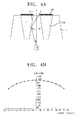
- Figures 4A and 4B are drawings describing the optical characteristics of a light guide in a PDP according to an exemplary embodiment of the present invention.
- the light guide 131 focuses and exits visible light generated from the discharge cell 115 using this feature.
- Equation 1 Na is the refractive index of the medium which fills the space 133, and Nf is the refractive index of the light guide 131. The lower the refractive index of the medium which fills the space 133, the higher the critical angle ⁇ is obtained.
- the refraction index of the space 133 is 1. In this condition, the light guide 131 meets total internal reflection conditions at maximum. This is because a medium of the minimum total internal reflection is a vacuum. If the space 133 is filled with air, the total internal reflection is 1.00029, so the total internal reflection condition of the light guide 131 is similar to that encountered in a vacuum. That is, a critical angle ⁇ lower than in any condition where the space 133 is filled with other material, not air, can be obtained. Accordingly, as the critical angle ⁇ gets lower, total internal reflection occurs well in spite of the low launch angle ⁇ .
- Figure 4B is a profile showing the distribution of luminance according to the visual angle ⁇ of visible light which has excited from the discharge cell 115. Visible light generated from the discharge cell 115 of the PDP is diffused light, which exits in all directions and distribution of luminance of which varies according to the visual angle ⁇ .
- Table 1 shows the correlation between the luminance and the launch angle ⁇ according to the visual angle ⁇ of the diffused light shown in Figure 4B.
- Visual angle (°) Luminance (%) launch angle (°) -70 72.7 16.73 -60 84.0 26.73 -50 90.4 36.73 -40 94.4 46.73 -30 96.7 56.73 -20 98.5 66.73 -10 100 76.73 0 100 86.73 10 100 76.73 20 98.5 66.73 30 96.7 56.73 40 94.4 46.73 50 90.4 36.73 60 84.0 26.73 70 72.7 16.73
- the luminance of the diffused light and launch angle ⁇ on the interface 131c vary according to the visual angle ⁇ . That is, the higher the absolute value of the visual angle ⁇ , the lower the luminance of the diffused light and the lower the launch angle ⁇ .
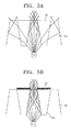
- Figures 5A and 5B are drawings describing the total internal reflection efficiency of a light guide in a PDP according to an exemplary embodiment of the present invention.
- Figure 5A shows total internal reflection in the light guide 131, when space between the light guides 131 is filled with a low refractive index medium 134.
- Figure 5B shows total internal reflection in the light guide 131, when space between the light guides 131 is implemented with the space 133 according to the exemplary embodiment of the present invention.
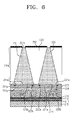
- Figure 6 shows the structure of a PDP according to another exemplary embodiment of the present invention.
- a PDP according to another exemplary embodiment of the present invention has the same structure as Figure 2, except that the light guide 231 is perpendicular to an address electrode 211.
- the address electrode 211, a first dielectric layer 212, a dam (not shown) and a phosphor layer 214 are disposed on a lower substrate 210.
- An upper substrate 230 includes the light guide 231 which is perpendicular to the address electrode 211, an external light blocking member 232 between exit surfaces 231b of the light guides 231, and a space 233 surrounded by the light guides 231 and the external light blocking member 232.
- a pair of discharge electrodes 221a and 221b, a pair of bus electrodes 222a and 222b, a second dielectric layer 223 and a protection layer 224 are disposed under the upper substrate 230.
- the lower substrate 210 and the upper substrate 230 are separated from each other, so a plurality of discharge cells 215 are formed for plasma discharge.
- the discharge cell 215 is filled with discharge gas, which is a mixture of neon (Ne) and a small amount of Xenon (Xe).
- discharge gas which is a mixture of neon (Ne) and a small amount of Xenon (Xe).
- Ne neon
- Xe Xenon
- visible light generated from the discharge cell 115 is received through an incidence surface 231a and focused so as to exit through the exit through surface 231b.
- Figure 7 shows a filter which is employed to enhance the bright room contrast of a PDP according to yet another exemplary embodiment of the present invention.
- the PDP of Figure 7 has the same structure as a conventional PDP, as shown in Figure 1, and the PDP is partially incised and has an upper substrate 320 rotated 90°.
- An address electrode 311, a first dielectric layer 312, a dam 313 and a phosphor layer 314 are disposed on a lower substrate 310.
- a pair of sustaining electrodes 321a and 321b, a pair of bus electrodes 322a and 322b, a second dielectric layer 323 and a protection layer 324 are disposed under the upper substrate 320.
- the lower substrate 310 and the upper substrate 320 are separated by a predetermined space and sealed to form discharge cells 315.
- a filter 330 is disposed on the upper substrate 320 to focus and emit visible light generated from the discharge cells 315.
- the filter 330 comprises a light guide 331 in which the incidence surface 331a is wider than the exit surface 331b, and an external light blocking member 332 between the exit surfaces 331b.
- a space 333 which is surrounded by the light guide 331 and the external light blocking member 332, is formed in the filter 330 and is filled with gases, such as air.
- gases such as air.
- the light guide 331 can be configured so that one light guide 331 corresponds to one discharge cell 315 as shown in Figure 7, or can be configured so that several light guides 331 correspond to one discharge cell 315.
- the light guide 331 can be produced with a width of less than a few tens of micrometers, it can be employed in a display device for high precision images.
- the exit surface 331b of the light guide 331 is processed with a non-glare treatment, so it can prevent glare by reflecting external light from the exit surface 331b of the light guide 331.
- the filter 330 can be bonded on the upper substrate 320 in a film form.
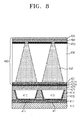
- Figure 8 shows components added to the PDP of Figure 2.
- the PDP of Figure 8 has the same basic structure as that of Figure 2. That is, an address electrode 411, a first dielectric layer 412, a plurality of dams 413 and a phosphor layer 414 are disposed on a lower substrate 410. A discharge cell 415 is filled with discharge gas. Discharge electrodes 421a (and 421b, not shown), bus electrodes 422a (and 422b, not shown), a second dielectric layer 423 and a protection layer 424 are disposed under an upper substrate 430.
- the upper substrate 430 comprises a near infrared blocking layer 431 which blocks near infrared rays closest to visible light among the light rays generated from the discharge cell 415, and enhances color purity.
- a light guide 432 is disposed on the near infrared blocking layer 431, and an external light blocking member 433 is formed between exit surfaces of the light guides 432 to block external light from entering the discharge cell 415.
- a space 436 is formed surrounded by the light guide 432 and the external light blocking member 433.
- An electromagnetic interference (EMI) prevention layer 434 which prevents EMI, is disposed on the exit surface of the light guide 432 and the external light blocking member 433 as a mesh manner or conductive film.
- An antireflection layer 435 is disposed on the EMI prevention layer 434 to prevent external light from being reflected and is implemented as an anti-reflective (AR) film.
- the light guides 432 can be configured so that one light guide corresponds to one discharge cell 415 as shown in Figure 2, or can be configured so that one light guide corresponds to several discharge cells 415.
- the near infrared blocking layer 431, the light guide 432, the external light blocking member 433, the EMI prevention layer 434 and the antireflection layer 435 can be disposed differently.
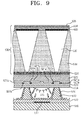
- Figure 9 shows components added to a filter which is employed to enhance the bright room contrast of the PDP of Figure 7.
- the PDP of Figure 9 has the same structure as a conventional PDP, as shown in Figure 1, and the PDP is partially incised and has an upper substrate 520 rotated at 90°.
- An address electrode 511, a first dielectric layer 512, a dam 513 and a phosphor layer 514 are disposed on a lower substrate 510.
- a pair of sustaining electrodes 521a and 521b, a pair of bus electrodes 522a and 522b, a second dielectric layer 523 and a protection layer 524 are disposed under the upper substrate 520.
- the lower substrate 510 and the upper substrate 520 are separated by a predetermined space and sealed to form discharge cells 515.
- a filter 530 is disposed on the upper substrate 520 to focus and emit visible light generated from the discharge cells 515 and to block light from the outside.
- the filter 530 comprises a near infrared blocking layer 531 which blocks near infrared rays closest to visible light among light rays generated by the discharge cell 515, and enhances color purity.
- a light guide 532 is disposed on the near infrared blocking layer 531, and an external light blocking member 533 is formed between exit surfaces of the light guides 532 to block light from the outside into the discharge cell 515.
- a space 536 is formed surrounded by the light guide 532 and the external light blocking member 533.
- An electromagnetic interference (EMI) prevention layer 534 which prevents EMI, is disposed on the exit surface of the light guide 532 and the external light blocking member 533 as a mesh or a conductive film.
- An antireflection layer 535 is disposed on the EMI prevention layer 534 to prevent external light from being reflected, and is implemented as an anti-reflective (AR) film.
- the light guides 532 can be configured so that one light guide 532 corresponds to one discharge cell 515 as shown in Figure 9, or can be configured so that several light guides 532 correspond to one discharge cell 515.
- the near infrared blocking layer 531, the light guide 532, the external light blocking member 533, the EMI prevention layer 534 and the antireflection layer 535 can be located differently.
- the filter 530 may be bonded on the upper substrate 520 as a film.
- the upper substrates 130, 230 and 430 of Figures 2, 6 and 8 and the filters 330 and 530 of Figures 7 and 9 can be bonded on the PDP as a film.
- the bright room contrast of the PDP can be enhanced by improving the capability of totally reflecting visible light generated from the discharge cell.
Landscapes
- Physics & Mathematics (AREA)
- Engineering & Computer Science (AREA)
- Plasma & Fusion (AREA)
- Electromagnetism (AREA)
- Gas-Filled Discharge Tubes (AREA)
- Devices For Indicating Variable Information By Combining Individual Elements (AREA)
Applications Claiming Priority (1)
| Application Number | Priority Date | Filing Date | Title |
|---|---|---|---|
| KR1020060053851A KR100740227B1 (ko) | 2006-06-15 | 2006-06-15 | 디스플레이 패널 |
Publications (3)
| Publication Number | Publication Date |
|---|---|
| EP1868223A2 true EP1868223A2 (de) | 2007-12-19 |
| EP1868223A3 EP1868223A3 (de) | 2008-12-10 |
| EP1868223B1 EP1868223B1 (de) | 2012-06-06 |
Family
ID=38498868
Family Applications (1)
| Application Number | Title | Priority Date | Filing Date |
|---|---|---|---|
| EP07102390A Not-in-force EP1868223B1 (de) | 2006-06-15 | 2007-02-14 | Anzeigetafel |
Country Status (4)
| Country | Link |
|---|---|
| US (1) | US8058804B2 (de) |
| EP (1) | EP1868223B1 (de) |
| KR (1) | KR100740227B1 (de) |
| CN (1) | CN101090055A (de) |
Cited By (1)
| Publication number | Priority date | Publication date | Assignee | Title |
|---|---|---|---|---|
| US6197126B1 (en) | 1992-03-31 | 2001-03-06 | Henkel Kommanditgesellschaft Auf Aktien | Nickel-free phosphating process |
Families Citing this family (4)
| Publication number | Priority date | Publication date | Assignee | Title |
|---|---|---|---|---|
| KR100937964B1 (ko) | 2008-12-01 | 2010-01-21 | 삼성에스디아이 주식회사 | 디스플레이 장치 및 광학 필터 |
| CN103968333A (zh) * | 2014-04-24 | 2014-08-06 | 京东方科技集团股份有限公司 | 聚光膜以及显示装置 |
| US20160178812A1 (en) * | 2014-12-19 | 2016-06-23 | Industrial Technology Research Institute | Optical film and display assembly applying the same |
| CN121399716A (zh) * | 2024-05-13 | 2026-01-23 | 京东方科技集团股份有限公司 | 显示面板和显示装置 |
Citations (1)
| Publication number | Priority date | Publication date | Assignee | Title |
|---|---|---|---|---|
| WO2005104167A1 (en) | 2004-04-27 | 2005-11-03 | Samsung Electronics Co., Ltd. | Plasma display panel |
Family Cites Families (9)
| Publication number | Priority date | Publication date | Assignee | Title |
|---|---|---|---|---|
| JPH08138559A (ja) * | 1994-11-11 | 1996-05-31 | Hitachi Ltd | プラズマディスプレイ装置 |
| US5608286A (en) * | 1994-11-30 | 1997-03-04 | Texas Instruments Incorporated | Ambient light absorbing face plate for flat panel display |
| US6636355B2 (en) | 2000-12-27 | 2003-10-21 | 3M Innovative Properties Company | Microstructured rear projection screen |
| EP1449016B1 (de) * | 2001-11-12 | 2007-06-06 | Koninklijke Philips Electronics N.V. | Filter zur kontraststeigerung und diesen filter verwendendes anzeigegerät |
| US7327083B2 (en) * | 2003-06-25 | 2008-02-05 | Samsung Sdi Co., Ltd. | Plasma display panel |
| US7050227B2 (en) * | 2003-12-11 | 2006-05-23 | 3M Innovative Properties Company | Composition for microstructured screens |
| KR100738814B1 (ko) | 2004-12-09 | 2007-07-12 | 엘지전자 주식회사 | 플라즈마 표시 장치용 필터 및 이를 포함한 플라즈마 표시 장치 |
| KR100629207B1 (ko) * | 2005-03-11 | 2006-09-27 | 주식회사 동진쎄미켐 | 전계 구동 차광형 표시 장치 |
| KR20070117162A (ko) * | 2006-06-07 | 2007-12-12 | 삼성전자주식회사 | 디스플레이 패널 |
-
2006
- 2006-06-15 KR KR1020060053851A patent/KR100740227B1/ko not_active Expired - Fee Related
-
2007
- 2007-02-12 CN CNA2007100055574A patent/CN101090055A/zh active Pending
- 2007-02-14 EP EP07102390A patent/EP1868223B1/de not_active Not-in-force
- 2007-03-19 US US11/723,251 patent/US8058804B2/en not_active Expired - Fee Related
Patent Citations (1)
| Publication number | Priority date | Publication date | Assignee | Title |
|---|---|---|---|---|
| WO2005104167A1 (en) | 2004-04-27 | 2005-11-03 | Samsung Electronics Co., Ltd. | Plasma display panel |
Cited By (1)
| Publication number | Priority date | Publication date | Assignee | Title |
|---|---|---|---|---|
| US6197126B1 (en) | 1992-03-31 | 2001-03-06 | Henkel Kommanditgesellschaft Auf Aktien | Nickel-free phosphating process |
Also Published As
| Publication number | Publication date |
|---|---|
| CN101090055A (zh) | 2007-12-19 |
| US20070290946A1 (en) | 2007-12-20 |
| KR100740227B1 (ko) | 2007-07-18 |
| US8058804B2 (en) | 2011-11-15 |
| EP1868223B1 (de) | 2012-06-06 |
| EP1868223A3 (de) | 2008-12-10 |
Similar Documents
| Publication | Publication Date | Title |
|---|---|---|
| CN100447932C (zh) | 等离子体显示板 | |
| EP1868223B1 (de) | Anzeigetafel | |
| KR100724057B1 (ko) | 플라즈마 디스플레이 패널 | |
| EP1745498B1 (de) | Plasmaanzeigetafel | |
| KR100793964B1 (ko) | 디스플레이 패널 | |
| EP1585161A2 (de) | Plasmaanzeigetafel | |
| US20070285790A1 (en) | Display panel | |
| CN1763897A (zh) | 等离子显示板 | |
| KR100797409B1 (ko) | 명암비 향상 필름 및 이를 포함하는 플라즈마 디스플레이패널 | |
| KR100804692B1 (ko) | 플라즈마 디스플레이 패널 | |
| KR100659068B1 (ko) | 플라즈마 디스플레이 패널 | |
| KR100615289B1 (ko) | 플라즈마 디스플레이 패널 | |
| CN1767130A (zh) | 等离子体显示面板 | |
| EP1667195A2 (de) | Plasmaanzeigetafel | |
| JP2002373589A (ja) | ガス放電パネルおよびその製造方法 | |
| US20080238313A1 (en) | Plasma display panel | |
| US20080211739A1 (en) | Plasma display panel | |
| KR20050101430A (ko) | 플라즈마 디스플레이 패널 | |
| KR20080039650A (ko) | 플라즈마 디스플레이 패널 | |
| KR20070047432A (ko) | 플라즈마 디스플레이 패널 | |
| KR20070055294A (ko) | 플라즈마 디스플레이 패널 |
Legal Events
| Date | Code | Title | Description |
|---|---|---|---|
| PUAI | Public reference made under article 153(3) epc to a published international application that has entered the european phase |
Free format text: ORIGINAL CODE: 0009012 |
|
| AK | Designated contracting states |
Kind code of ref document: A2 Designated state(s): AT BE BG CH CY CZ DE DK EE ES FI FR GB GR HU IE IS IT LI LT LU LV MC NL PL PT RO SE SI SK TR |
|
| AX | Request for extension of the european patent |
Extension state: AL BA HR MK YU |
|
| PUAL | Search report despatched |
Free format text: ORIGINAL CODE: 0009013 |
|
| AK | Designated contracting states |
Kind code of ref document: A3 Designated state(s): AT BE BG CH CY CZ DE DK EE ES FI FR GB GR HU IE IS IT LI LT LU LV MC NL PL PT RO SE SI SK TR |
|
| AX | Request for extension of the european patent |
Extension state: AL BA HR MK RS |
|
| RIC1 | Information provided on ipc code assigned before grant |
Ipc: H01J 17/16 20060101ALI20081104BHEP Ipc: H01J 17/49 20060101AFI20070927BHEP |
|
| 17P | Request for examination filed |
Effective date: 20090513 |
|
| 17Q | First examination report despatched |
Effective date: 20090615 |
|
| AKX | Designation fees paid |
Designated state(s): DE FR GB NL |
|
| GRAP | Despatch of communication of intention to grant a patent |
Free format text: ORIGINAL CODE: EPIDOSNIGR1 |
|
| GRAS | Grant fee paid |
Free format text: ORIGINAL CODE: EPIDOSNIGR3 |
|
| GRAA | (expected) grant |
Free format text: ORIGINAL CODE: 0009210 |
|
| AK | Designated contracting states |
Kind code of ref document: B1 Designated state(s): DE FR GB NL |
|
| REG | Reference to a national code |
Ref country code: GB Ref legal event code: FG4D |
|
| REG | Reference to a national code |
Ref country code: DE Ref legal event code: R096 Ref document number: 602007023108 Country of ref document: DE Effective date: 20120802 |
|
| REG | Reference to a national code |
Ref country code: NL Ref legal event code: T3 |
|
| RAP2 | Party data changed (patent owner data changed or rights of a patent transferred) |
Owner name: SAMSUNG ELECTRONICS CO., LTD. |
|
| PLBE | No opposition filed within time limit |
Free format text: ORIGINAL CODE: 0009261 |
|
| STAA | Information on the status of an ep patent application or granted ep patent |
Free format text: STATUS: NO OPPOSITION FILED WITHIN TIME LIMIT |
|
| 26N | No opposition filed |
Effective date: 20130307 |
|
| REG | Reference to a national code |
Ref country code: DE Ref legal event code: R097 Ref document number: 602007023108 Country of ref document: DE Effective date: 20130307 |
|
| REG | Reference to a national code |
Ref country code: FR Ref legal event code: ST Effective date: 20131031 |
|
| PG25 | Lapsed in a contracting state [announced via postgrant information from national office to epo] |
Ref country code: FR Free format text: LAPSE BECAUSE OF NON-PAYMENT OF DUE FEES Effective date: 20130228 |
|
| PGFP | Annual fee paid to national office [announced via postgrant information from national office to epo] |
Ref country code: DE Payment date: 20140211 Year of fee payment: 8 Ref country code: NL Payment date: 20140213 Year of fee payment: 8 |
|
| PGFP | Annual fee paid to national office [announced via postgrant information from national office to epo] |
Ref country code: GB Payment date: 20140211 Year of fee payment: 8 |
|
| REG | Reference to a national code |
Ref country code: DE Ref legal event code: R119 Ref document number: 602007023108 Country of ref document: DE |
|
| REG | Reference to a national code |
Ref country code: NL Ref legal event code: V1 Effective date: 20150901 |
|
| PG25 | Lapsed in a contracting state [announced via postgrant information from national office to epo] |
Ref country code: NL Free format text: LAPSE BECAUSE OF NON-PAYMENT OF DUE FEES Effective date: 20150901 |
|
| GBPC | Gb: european patent ceased through non-payment of renewal fee |
Effective date: 20150214 |
|
| PG25 | Lapsed in a contracting state [announced via postgrant information from national office to epo] |
Ref country code: DE Free format text: LAPSE BECAUSE OF NON-PAYMENT OF DUE FEES Effective date: 20150901 Ref country code: GB Free format text: LAPSE BECAUSE OF NON-PAYMENT OF DUE FEES Effective date: 20150214 |