EP1868263A1 - Antenne transparente pour affichage, organe phototransmetteur pour affichage possedant une antenne, et element pour boitier, dote d une antenne - Google Patents
Antenne transparente pour affichage, organe phototransmetteur pour affichage possedant une antenne, et element pour boitier, dote d une antenne Download PDFInfo
- Publication number
- EP1868263A1 EP1868263A1 EP06730905A EP06730905A EP1868263A1 EP 1868263 A1 EP1868263 A1 EP 1868263A1 EP 06730905 A EP06730905 A EP 06730905A EP 06730905 A EP06730905 A EP 06730905A EP 1868263 A1 EP1868263 A1 EP 1868263A1
- Authority
- EP
- European Patent Office
- Prior art keywords
- antenna
- transparent
- antenna pattern
- section
- electrically conductive
- Prior art date
- Legal status (The legal status is an assumption and is not a legal conclusion. Google has not performed a legal analysis and makes no representation as to the accuracy of the status listed.)
- Withdrawn
Links
Images






Classifications
-
- H—ELECTRICITY
- H01—ELECTRIC ELEMENTS
- H01Q—ANTENNAS, i.e. RADIO AERIALS
- H01Q1/00—Details of, or arrangements associated with, antennas
- H01Q1/40—Radiating elements coated with or embedded in protective material
-
- H—ELECTRICITY
- H01—ELECTRIC ELEMENTS
- H01Q—ANTENNAS, i.e. RADIO AERIALS
- H01Q1/00—Details of, or arrangements associated with, antennas
- H01Q1/12—Supports; Mounting means
- H01Q1/22—Supports; Mounting means by structural association with other equipment or articles
- H01Q1/24—Supports; Mounting means by structural association with other equipment or articles with receiving set
- H01Q1/241—Supports; Mounting means by structural association with other equipment or articles with receiving set used in mobile communications, e.g. GSM
- H01Q1/242—Supports; Mounting means by structural association with other equipment or articles with receiving set used in mobile communications, e.g. GSM specially adapted for hand-held use
- H01Q1/243—Supports; Mounting means by structural association with other equipment or articles with receiving set used in mobile communications, e.g. GSM specially adapted for hand-held use with built-in antennas
-
- H—ELECTRICITY
- H01—ELECTRIC ELEMENTS
- H01Q—ANTENNAS, i.e. RADIO AERIALS
- H01Q1/00—Details of, or arrangements associated with, antennas
- H01Q1/36—Structural form of radiating elements, e.g. cone, spiral, umbrella; Particular materials used therewith
- H01Q1/38—Structural form of radiating elements, e.g. cone, spiral, umbrella; Particular materials used therewith formed by a conductive layer on an insulating support
-
- H—ELECTRICITY
- H01—ELECTRIC ELEMENTS
- H01Q—ANTENNAS, i.e. RADIO AERIALS
- H01Q9/00—Electrically-short antennas having dimensions not more than twice the operating wavelength and consisting of conductive active radiating elements
- H01Q9/04—Resonant antennas
- H01Q9/0407—Substantially flat resonant element parallel to ground plane, e.g. patch antenna
-
- H—ELECTRICITY
- H01—ELECTRIC ELEMENTS
- H01Q—ANTENNAS, i.e. RADIO AERIALS
- H01Q9/00—Electrically-short antennas having dimensions not more than twice the operating wavelength and consisting of conductive active radiating elements
- H01Q9/04—Resonant antennas
- H01Q9/16—Resonant antennas with feed intermediate between the extremities of the antenna, e.g. centre-fed dipole
-
- H—ELECTRICITY
- H01—ELECTRIC ELEMENTS
- H01Q—ANTENNAS, i.e. RADIO AERIALS
- H01Q9/00—Electrically-short antennas having dimensions not more than twice the operating wavelength and consisting of conductive active radiating elements
- H01Q9/04—Resonant antennas
- H01Q9/30—Resonant antennas with feed to end of elongated active element, e.g. unipole
Definitions
- the present invention relates to a transparent antenna for a display, a translucent member for a display with an antenna and a housing component with an antenna composed so as to receive terrestrial broadcasting and satellite broadcasting or to transmit and receive radio which are attached to a display screen of a television monitor, a mobile terminal such as a cellular phone handset or built in a housing of a cellular phone handset as a part thereof.
- a loop antenna, a rod antenna and the like have been conventionally known, and these antennas are placed near a television to be connected to the television via an antenna cable.
- an antenna for mobile devices such as mobile phone and the like
- a rod-shaped miniaturized antenna protruded from a body of the mobile phone is commonly used (For example, refer to Japanese Unexamined Patent Application Publication No. 2004-207880 ).
- the loop antenna and the rod antenna are bulky and are not good in terms of appearance and design, and are inconvenient in carrying.
- an antenna for mobile devices is required to respond to various communication frequencies such as television, radio broadcasting, GPS (global positioning system), RFID (radio frequency identification), and Bluetooth in addition to having functions of telephone, internet communication and the like, so a plurality of antennas are required.
- GPS global positioning system
- RFID radio frequency identification
- Bluetooth radio frequency identification
- a space to be allocated to one antenna is becoming even smaller.
- a main object of the present invention is to provide a transparent antenna for a display, a translucent member for a display with an antenna and a housing component with an antenna which is capable of good transmission and reception which is not bulky and does not damage design of the device.
- a transparent antenna for a display according to the present invention comprises a sheet-like transparent substrate having an electrical isolation, an antenna pattern formed on a surface of the transparent substrate in a planar form, characterized in that an electrically conductive part of the antenna pattern comprises an electrically conductive thin film of a mesh structure, outlines of each mesh comprise extra fine bands having substantially equal width and that a light transmittance of the antenna pattern formation section is 70 % or more.
- the transparent antenna for a display of the present invention is composed so as to be attached planarity on a display screen of a television, a mobile phone and the like.
- a display screen of a television, a mobile phone and the like is composed so as to be attached planarity on a display screen of a television, a mobile phone and the like.
- miniaturized mobile devices such as a mobile phone
- a proportion of the display is relatively large compared to a body size thereof
- an antenna is attached by effectively utilizing an area of the display.
- a front surface of the display which has not been conventionally regarded as an antenna-setting space is used as an antenna-setting space.
- a transparent antenna for a display of the present invention since an electrically conductive part constituting the antenna pattern is formed into a mesh structure having a multitude of apertures, and outlines of each mesh are composed of extra fine bands, there is an advantage that the antenna pattern is recognized only as a slight variation of shading when looking at the display screen through the transparent antenna for a display.
- a light transmittance is more preferably 80 % or more.
- a transparent electrically conductive film such as ITO (indium tin oxide) as an antenna on a front surface of the display
- the transparent electrically conductive film has a property that as a film thickness thereof becomes thinner and a degree of transparency becomes higher, surface resistance thereof as an indicator of electrical conductivity becomes larger. Therefore, there is a situation that it is difficult to obtain low resistivity required for an antenna while securing transparency.
- resistivity of a transparent electrically conductive film with transparency secured has a resistivity of a few dozen to a few hundreds ⁇ , a resistance value required for an antenna must be very small, as small as 3 ⁇ or less.
- a mesh structure which is an assembly of extra fine bands of the present invention can achieve low resistivity which is required for an antenna while securing transparency.
- a subject-matter of the present invention is that the antenna pattern is set in a mesh shape, a mesh pitch and a bias angle which do not form a moire pattern with a mesh pattern which forms a picture element of the display.
- a distinguish pattern can be distinguished from the antenna pattern if the mesh structure comprises a plane mesh in which a mesh having a same shape and size continues regularly on a plane surface, and in a part of the antenna pattern, the distinguishing pattern is added to an inner part of a plurality of the meshes in a linear form, or to outlines of a plurality of the meshes in a band-like form, since an amount of light that passes through those meshes becomes less than an amount of light that passes through the antenna pattern.
- the distingushing pattern can be formed by using thicker bands for the outline of the mesh constituting the plane mesh. Also, it can be formed by shifting a part of the mesh pattern of the mesh structure on the antenna pattern within a range that does not exceed a size of one mesh and overlapping it on the antenna pattern. If such a distinguishing pattern is formed continuously or intermittently on the antenna pattern, a letter and a design can be formed on the transparent antenna surface.
- the mesh structure is constituted of a plane mesh regularly continuing on a plane surface and a gradation section to reduce brightness difference formed between an antenna pattern and an antenna pattern non-formation section can be provided on a border region between the antenna pattern and the antenna pattern non-formation section of a transparent substrate.
- the gradation section can be formed by omitting a part of the outline of the mesh of the antenna pattern in the border region or by roughening the mesh.
- the gradation section can be formed by making the omitted width of the outline or a width of the aperture of the mesh longer gradually from the side of the antenna pattern toward the side of the antenna pattern non-formation section.
- the gradation section can be formed by positioning a vertical direction electrically conductive wire and a transverse direction electrically conductive wire in a lattice like state to constitute a mesh structure and omitting a part of those, at least either vertical direction electrically conductive wire or transverse direction electrically conductive wire, or by enlarging spacing between the electrically conductive wires from a side of the antenna pattern toward a side of the antenna pattern non-formation section.
- the antenna pattern can be formed into a continuous band-like state by having a slit in a part of the mesh structure. However, it is to be within a range that the width of the slit does not exceed a maximum size of the mesh size.
- the antenna pattern can be formed in a meandering shape, in order to elongate the effective length of the antenna, by forming a plurality of slits in a predetermined length alternatively from different directions in a mesh structure. Further, the antenna pattern can be formed by forming one slit in a spiral form toward the center of the mesh structure.
- a maximum size of the mesh is preferably to be 1 mm.
- a shape of the meshes may be constituted of geometric designs.
- the present invention excludes those of geometric designs in which the lines of the meshes are not constructed from extra fine bands even if the antenna pattern has a geometric design such as circles and ellipses.
- the width of the each of the extra fine bands is preferably 30 ⁇ m or less, since if the width of each of the extra fine bands is thin, the presence of the extra fine bands is hard to recognize.
- the antenna pattern can be composed of extra fine metal wires made of copper or a copper alloy.
- a transparent protection film is preferably formed on a surface of the antenna pattern, since a damage of the antenna pattern can be prevented by the transparent protection film.
- a preferred constitution is that a part of the electrically conductive part is equipped with an electrode for power supply and a transparent protection film corresponding to the electrode is provided with a through hole part to expose the electrode.
- a surface of the extra fine bands is preferably subjected to low reflection treatment. Even if a material of the extra fine bands gives off a metallic luster, the low reflection treatment reduces the luster so that it becomes inconspicuous.
- a transparent adhesive layer can be formed on a face of opposite the electrically conductive part forming side of the transparent substrate. In this manner, the transparent antenna for a display of the present invention will be easily attached afterwards on a front surface of the display.
- a feature of the translucent member for a display with an antenna of the present invention is that a transparent antenna for a display equipped with electrodes for power supply in a part of the electrically conductive part is interposed between two pieces of translucent plate material for a display in a state in which the electrodes are projected.
- the translucent plate material for the display includes a plate material made of transparent synthetic resin such as a protection panel generally used for an outermost surface of the display, and, in addition, it may also be a glass.
- the translucent member for a display with an antenna of the present invention can be obtained, for example, by making a protection panel for a display composed of a two layer structure and embedding a transparent antenna in the bonding face of the two protection panels during the process of manufacturing.
- the translucent member for a display with an antenna By the translucent member for a display with an antenna, a step equivalent to a thickness of the transparent antenna is not formed on a surface of the display just as in a case where an antenna is attached afterwards, so that design can be further improved. Additionally, a stable antenna performance can be ensured by embedding the antenna between translucent members for display with an antenna.
- the transparent antenna for a display and the translucent plate material for a display are integrated by injection molding. In this way, unity of the transparent antenna for a display and the translucent plate material for a display will be improved.
- the transparent antenna for a display and the translucent member for a display with an antenna described above are used, since a display screen can be used effectively as an antenna setting space, it will be unnecessary to secure an antenna-setting space separately, and particularly when applied to a mobile device, miniaturization thereof will be possible.
- a good display condition can be obtained without lowering visibility. Further, it does not damage design of the device, not bulky, and offer a good antenna performance. Additionally, it will be possible to mount a plurality of antennas without damaging design of the device, so it is effective for miniaturizing the device as well as enhancing performance of the device.
- a feature of the housing component woth an antenna of the present invention is that a housing component comprises a molded resin material as a main constituting layer and has an opaque decorative part in a part or an entire part thereof, and a front surface side of a layer giving a decoration of the opaque decorative part has an antenna pattern in a planar form having a light transmittance of 70 % or more, and an electrically conductive part of the antenna pattern is composed of an electrically conductive thin film of a mesh structure, and outlines of each mesh are composed of extra fine bands having substantially an equal width, and it is equipped with an electrode for power supply for the antenna pattern.
- a feature of another housing component with an antenna of the present invention is that a housing component having an antenna comprises a molded resin material as a main constituting layer, and a transparent decorative part in a part or an entire part thereof with which a decorative effect can be obtained by illumination from a back side, and the transparent decorative part has an antenna pattern in a planar form having a light transmittance of 70 % or more , and the electrically conductive part of the antenna pattern is composed of an electrically conductive thin film of a mesh structure, and outlines of each mesh are composed of extra fine bands having substantially an equal width, and it is equipped with an electrode for power supply for the antenna pattern.
- a feature of still another housing component with an antenna of the present invention is that the housing component with an antenna comprises a molded resin material as a main constituting layer and a transparent decorative part giving a decorative effect by illumination from a side surface in a part or an entire part thereof, and a front surface side of the molded resin material of the transparent decorative part has an antenna pattern in a planar form having a light transmittance of 70 % or more, and an electrically conductive part of the antenna pattern is composed of an electrically conductive thin film of a mesh structure, and outlines of each mesh are composed of extra fine bands having substantially an equal width, and is equipped with an electrode for power supply for the antenna pattern.
- the housing component with an antenna if the housing component with an antenna has a transparent window part for a display other than the decorative part, the antenna pattern can be extended up to the transparent window part.
- the housing component with an antenna includes a transparent window part and a window cover consisting only of a window frame section thereof.
- the antenna pattern is extended up to the transparent window part as described above, a relatively large area of the front surface of the display can be used when a plurality of antennas are mounted to the device, so that the antennas can be mounted without damaging design.
- the housing component with an antenna can also function as a window cover.
- the antenna pattern extended up to the transparent window part is preferably set in a mesh shape, a mesh pitch, and a bias angle which do not form a moire pattern with a mesh pattern that forms pixels of the display.
- a part of the electrically conductive part of the antenna pattern can be used as the electrode for power supply.
- an electrically conductive part of the antenna pattern is formed into a mesh structure having a number of apertures, and since outlines of each mesh are composed of extra fine bands, when looking at an opaque decorative section and an illumination-decoration section where a decorative effect can be obtained by illumination, the antenna pattern is recognized only as a slight variation of shading, so that a design provided on the housing is not damaged by the attached antenna. Further, a front surface of a relatively large display can be used for a space for mounting the antenna so that receiver sensitivity can be improved and good transmission and reception are made possible.
- the light transmittance is preferably 80 % or more.
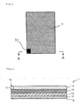
- Fig. 1 is a schematic diagram showing a state in which the transparent antenna for a display (hereinafter abbreviated as transparent antenna) 1 according to a first embodiment of the present invention is attached to a display screen 3 of a cellular phone handset 2.
- transparent antenna for a display
- the cellular phone handset 2 is a two-folded type handset equipped with a display screen (sub window) 3 on an outer surface when it is folded.
- a transparent antenna 1 is attached on an entire display area of the display screen 3.
- An electrode for power supply of the transparent antenna 1 is connected to a transmission and reception section in the cellular phone handset 2 via an input-output terminal disposed on an outer frame of the display screen 3.
- the transparent antenna 1 having an antenna pattern by an electrically conductive part 1b is formed on a transparent plastic sheet 1 as a transparent substrate having an electrical isolation.
- An outer shape of the transparent antenna 1 is a rectangular shape substantially corresponding to a size of the display screen 12.
- a transparent resin film or a plate material such as polycarbonate, an acrylic resin, polyethylene terephthalate and triacetyl cellulose may be used.
- a transparent substrate a sheet-like transparent glass may also be used.
- the electrically conductive part 1b comprises an electrically conductive thin film of a mesh structure, and a metal thin film of copper, nickel, aluminum, gold, silver and the like or an electrically conductive resin paste film containing metallic particulates or carbon particulates of those may be used.
- the electrode part 1c is provided to come in contact with the input-output terminal disposed on an outer frame of the display screen 3 of the cellular phone handset 2, and the electrode part 1c is formed in a square-shaped sheet electrically connected to the electrically conductive part 1b.
- a photoresist film is formed on a metal thin film or an electrically conductive resin paste film (hereinafter, these are occasionally referred to as metal thin film for convenience of explanation) to be subjected to exposure by photomask and development using a liquid developer, thereby forming an antenna pattern of a resist film.
- an extra fine metal wire including an extra fine electrically conductive resin wire formed of an electrically conductive resin paste film; hereinafter the same.
- the antenna pattern of the resist film is printed on the metal thin film by a method such as screen printing, gravure printing, and ink-jet printing, and the metal thin film except for a resist-covered section is subjected to etching using an etchant, followed by separation of resist film, thereby forming the antenna pattern of the metal thin film.
- the antenna pattern is formed by printing of an electrically conductive resin paste
- the antenna pattern is printed on a transparent substrate material using an electrically conductive resin paste and a carbon resin paste and the like containing metal particulates, thereby forming an electrical conductive antenna pattern.
- Printing methods used herein include screen printing, gravure printing, ink-jet printing and the like, same as described above.
- a surface of the extra fine bands formed on the mesh-shaped pattern is subjected to low reflection treatment, reflected colors of the metal and the like are suppressed so that the presence of the transparent antenna 1 becomes inconspicuous. In this way, visibility when looking at the display screen 3 through a mesh-shaped pattern is enhanced. Additionally, it can be expected that a contrast in the display screen 3 is increased and an image quality is improved.
- the low reflection treatment include a surface treatment such as a chemical conversion treatment and plating.
- the chemical conversion treatment is a treatment wherein a low-reflection layer is formed on a surface of a metal by oxidation treatment or sulfurization treatment, and for example, if copper is used for a material of the extra fine metal wire, and an oxide film is formed on a surface thereof by oxidation, the surface of the extra fine metal wire can be treated so as to be in black color having an antireflection quality without reducing a section size of the extra fine metal wire.
- a surface of the extra fine metal wire can be treated to be colored black having an antireflection quality. If it is subjected to copper plating with high current density, it can be treated to be colored brownish-red.
- the electrically conductive part 1b is formed on the transparent plastic sheet (transparent base) 1a, and the electrically conductive part 1b is covered with a transparent cover layer (transparent protection film) 1d.
- an under surface side of the transparent antenna 1 may be attached facing the display screen 3, or an upper surface side of the transparent antenna 1 may also be attached facing the display screen 3.
- the transparent antenna 1 is attached facing the display screen 3, since the transparent plastic sheet (transparent substrate) 1a functions for protecting the electrically conductive part 1b just like the transparent cover layer 1d, the transparent cover layer 1d may be omitted.
- a transparent adhesive layer 1f may be provided on a surface of the electrically conductive part 1b
- the transparent cover layer 1d protects the electrically conductive part 1b, so that a stable antenna performance can be maintained even if surrounding environment of the cellular phone handset 2 to which the transparent antenna 1 is attached, such as temperature and humidity is changed. Additionally, the antenna pattern also becomes less susceptible to scratches due to existence of the transparent cover layer 1d.
- the transparent cover layer 1d for example, it can be formed by attaching the transparent film on an antenna pattern comprising the electrically conductive part 1b using a transparent adhesive or a pressure sensitive adhesive, and also by applying a transparent resin on the antenna pattern in a predetermined thickness.
- a through hole part 1e is provided in a part of the transparent cover layer 1d, and an electrode part 1c is exposed through the through hole part 1e.
- the input-output terminal and the antenna wire provided on the outer frame of the display screen 3 are connected to the electrode part 1c which is exposed.
- a transparent adhesive layer 1f is attached on an opposite surface of the electrically conductive part 1b of the transparent plastic sheet 1a, and a separating sheet 1g is attached on a surface of the transparent adhesive layer 1f.
- the transparent adhesive layer 1f one that does not damage transparency of an antenna such as a transparent acrylic adhesive and the like may be used.
- the separating sheet 1g is separated to expose the transparent adhesive layer 1f, and the transparent antenna 1 is attached on a front surface of the display screen 3 via the transparent adhesive layer 1f.
- the transparent antenna 1 having the above structure may be attached on a front surface of various displays including the television monitor screen, display screen of a personal computer and the like in addition to the display screen 3 of the cellular phone handset 2.
- the transparent antenna 1 is interposed between two pieces of translucent plate material for a display.
- the translucent plate material for a display include a plate material made from a transparent synthetic resin such as a transparent acrylic plate and a transparent polycarbonate plate.
- the translucent member denotes a member having light transparency which is substantially transparent.
- the transparent antenna 1 When the transparent antenna 1 is embedded between the translucent plate material pieces, the transparent antenna 1 is integrated with two translucent plate material pieces, so that the transparent adhesive layer 1f is not an indispensable.
- the transparent cover layer 1d may be formed as required.
- a through hole part is provided in a position which is a part of the translucent plate material for a display and corresponds to the through hole part 1e so that the electrode part 1c is exposed through the through hole part.
- the input-output terminal and the antenna wire attached to the outer frame of the display screen 3 are connected to the electrode part 1c.
- injection molding may be employed, so that a molten resin is discharged in a paste and the transparent antenna 1 is interposed between the discharged resin.
- the transparent antenna 1 is interposed between two pieces of the translucent plate material for a display to be integrated.
- the transparent antenna 1 is inserted by injection molding, a translucent plate material for a display having a three-dimensional curve may also be easily formed. Accordingly, it can be attached when the display screen 3 is in a shape of having a three-dimensional curve.
- the transparent antenna 1 may be used instead of a conventional display protection panel.
- a translucent plate material for a display which has been subjected to low reflection treatment is used, visibility of a display items on the display screen 3 can be enhanced.
- Figs. 4 to 6 show an enlarged view of a part of the antenna pattern of the transparent antenna.
- the antenna pattern shown in Fig. 4 is formed into a lattice-shaped mesh, having a linear shaped electrically conductive partlb extended in X direction and Y direction wherein a light transmittance in the transparent antenna 1 is ensured to be 70 % or more.
- the above-mentioned light transmittance which is a gauge of the transparency means the total light transmittance with respect to total amount of light having entire of wavelength emitted from a light source having a specific color temperature which has transmitted through a surface of a specimen. If the light transmittance becomes lower than 70 %, an image of the display viewed through the transparent antenna 1 becomes darker, damaging an image quality thereof. On the other hand, if the transmission is excessively enhanced, a preferable antenna performance (such as surface resistance value) cannot be obtained; thus, this point should be taken into consideration in setting the transmittance.
- the above-mentioned light transmittance is measured using a spectrometer manufactured by Nippon Denshoku Industries Co., Ltd. (Model number NDH2000). However, 100 % of the light transmittance in air layer is defined as the standard.
- the light transmittance is measured in a state that the transparent cover layer 1d is included, and in the case where the transparent pressure adhesive layer 1f is provided, the light transmittance is measured in a state that the transparent pressure adhesive layer 1f is included.
- the wire widths w of the extra fine metal wire (extra fine band) 1i which shapes an outline of a square in X direction and a extra fine metal wire (extra fine band) l1 in Y direction are formed into an equal width of 30 ⁇ m or less, respectively. If each of the wire widths w becomes thicker than 30 ⁇ m, a mesh of the antenna pattern becomes outstandingly visible, and a design quality thereof becomes poorer. Furthermore, it becomes an obstacle for viewing an image in the display.
- the wire width w becomes 30 ⁇ m or less, a presence of the antenna pattern is hard to recognize so that display becomes easily viewable.
- a film thickness of the extra fine metal wire if an aspect ratio of the wire width/film thickness t becomes 0.5 or more, an antenna pattern having a high accuracy can be made easily.
- a light transmittance of the transparent antenna 1 is ensured to be 70 % or more by selecting combinations of the wire width of the extra fine metal wire 1i and 1j and a size of an aperture part B formed by being surrounded by these extra fine metal wires 1i and 1j.
- An antenna pattern shown in Fig. 5 is made to be mesh-like shape having a hexagonal shape as core and continuous in X-direction, Ya-direction and Yb-direction.
- the wire width w of the extra fine metal wire 1k forming the outlines of the hexagon is 30 ⁇ m or less.
- the antenna pattern shown in Fig. 6 is made to be a mesh-like shape having a ladder shape as a core and continuous in X-direction and Y-direction.
- the wire widths w of the extra fine metal wires 1l and 1m forming the outlines of the ladder shape are 30 ⁇ m or less, respectively.
- the antenna pattern may include those having continuous rectangular shapes as a core, those having continuous polygonal shapes as a core, and those having continuous ladder shapes as a core.
- a mesh shape of the transparent antenna pattern, a mesh pitch, and a bias angle are adjusted according to the size and shape of the picture element of the display.
- a convenient and easy method is to make several kinds of trial products and check an existence or nonexistence of the moire pattern by visual observation to determine a specification.
- those having continuous square shapes as a core are particularly preferable since it becomes hard to recognize the antenna pattern as stripes as compared with other polygonal shapes.
- the moire pattern denotes thick fringe streak which is visible when mesh-shaped patterns are overlapped due to a intervention of an upper and lower mesh.
- the lines tends to be seen in stripes continuous along the continuing cores (apertures).
- the lines of the above-mentioned extra fine bands along the continuous directions become zigzag and accordingly the lines are seemed to be thick to the extent corresponding to the fluctuation of the zigzag shape and as a result, the extra fine bands are seen in expanded state.
- the above-mentioned square shapes may include not only complete squares having stiff corners but also chamfered squares.
- a transparent resin layer containing a plating catalyst was formed to be subjected to electroless copper nickel plating, followed by electrolytic copper plating, thereby forming a metal thin film.
- both surfaces of the metal thin film were subjected to chemical conversion treatment(low reflection treatment). Then, an aperture was formed by photo-etching method on the metal thin film (to be an electrically conductive thin film of the mesh structure) to give an antenna pattern.
- the electrically conductive part 1b of this antenna pattern is a square mesh pattern shown by Fig. 4, and the extra fine band 1i thereof has a line width (w) of 15 ⁇ m, line space pitches of 400 ⁇ m, and a bias angle of 30°.
- a transparent polyethylene terephthalate cover film (transparent cover layer (transparent protection film ) 1d) subjected to low reflection treatment with a thickness of 125 ⁇ m was bonded on the electrically conductive part 1b of the antenna pattern using an acryl-based transparent adhesive.
- the electrode part 1c was exposed from an opening (through hole part 1e) formed by cutting a part of the cover film.
- a both side coated transparent acrylic type pressure sensitive adhesive film (transparent adhesive layer 1f) with a separating sheet for attaching the transparent antenna 1 on a display screen of a device was attached on an opposite side surface (backside) of the electrically conductive part 1b of the transparent polyethylene terephthalate film (transparent substrate 1a).
- an antenna pattern was formed on the transparent polyethylene terephthalate film, and was further covered with a cover film, and a laminated layer body in which the both side coated transparent acrylic type pressure sensitive adhesive film having a separating sheet was put on the backside of the transparent polyethylene terephthalate film was obtained; the outside of the laminated layer body was cut along the antenna pattern to produce the transparent antenna 1.
- a separating sheet 1g of the transparent antenna 1 was removed, and was attached on a screen of the liquid crystal display, and an antenna code was connected to the electrode part 1c which is exposed, and the antenna code was connected to a receiving part of a main unit of the liquid crystal display.
- a copper foil woth a thickness of 12 ⁇ m having both surfaces with lowered reflectance by chemical conversion treatment was bonded on a transparent polycarbonate film (transparent substrate 1a) having a thickness of 100 ⁇ m using a transparent adhesive, and subsequently an antenna pattern of a resist film was printed; after a copper foil except for a resist-covered section was subjected to etching using an etchant, the resist film was removed, thereby forming the antenna pattern.
- the antenna pattern has an electrically conductive part 1b in which a shape of a mesh aperture thereof is a regular hexagonal lattice pattern, 500 ⁇ m on a side, and a line width of a extra fine band 1k (refer to Fig. 5) was 25 ⁇ m.
- the transparent antenna 1 was inserted in a metal mold for a sub window protection panel of a cellular phone handset to feed a polycarbonate resin in the metal mold and carry out injection molding.
- sub window parts for a cellular phone handset in which a translucent plate material layer made from polycarbonate was positioned on front and back sides of the transparent antenna 1 was obtained.
- a structure in which an electrode part 1c was protruded from a surrounding of the translucent plate material was formed.
- a light transmittance of the resultant sub window parts having an antenna was 73 %.
- Sub window parts having an antenna were disposed on a sub window of the cellular phone handset, and an electrode part 1c was connected to an input-output terminal mounted on an outer frame of the sub window.
- a transparent antenna of the second embodiment is enabled to have letters and designs on an antenna pattern.
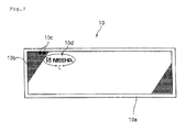
- a transparent antenna 10 shown in Fig. 7 comprises an antenna pattern as a electrically conductive section 10b planarly formed on a transparent plastic sheet 10a as an electrically insulating transparent base body and an antenna terminal 10c is formed in the left upper part of the antenna pattern formed transversely long rectangular shape.
- Reference symbol 10d shows logo designed on the transparent antenna 10 and the formation method of the logo will be described later.
- the above-mentioned transparent plastic sheet 10a is made of the same material as that of the transparent plastic sheet 1a shown in Fig. 3 and the above-mentioned electrically conductive section 10b is also made of the same material as that of the electrically conductive section 1b and has the same configuration.
- the above-mentioned antenna terminal 10c is for sticking the electric power supply section (not shown) of the antenna cord 4 and the antenna terminal 10c is constructed from a square sheet electrically connected with the mesh-like pattern.
- Fig. 8 is an enlarged view of a C part in Fig. 7.
- the logo 10d was formed on the mesh section 10e constructed from the electrically conductive section 10b and constructed by combining a letter section 10f and a letter shadow section 10g showing the shadow of the letter section 10f.
- the letter section 10f is constructed from a electrically conductive section (thick band) 10h of a electrically conductive wire with a wider width than that of the electrically conductive wire of the mesh section 10e and the aperture surface area of an aperture section 10j in the letter section 10f is adjusted to be smaller than the aperture surface area of the aperture section 10i, so that the light transmittance is changed and accordingly, the boundary of the mesh section 10e and the letter section 10f is emphasized to make the latter part outstanding.
- the letter shadow section 10g shown in Fig. 8 has the same width as that of the electrically conductive wire of the letter section 10f as being seen in further enlarged view of Fig. 10, however it is configured using the electrically conductive section 10k in a mesh pattern further denser than the letter section 10f and thus the aperture surface area of an aperture section 10m in the letter shadow section 10g is adjusted to be smaller than the aperture surface area of the aperture section 10j in the letter section 10f, so that the letter shadow section 10g can be emphasized.
- the aperture surface area of an aperture section 10m in the letter shadow section 10g is set to be about 3/4 to 1/4 of the aperture surface area of the letter section 10f.
- the letter section 10f and the letter shadow section 10g have a function as a distinguishing pattern for recognizing a part of the antenna pattern by decreasing a prescribed quantity of the light passing through the meshes.
- the letter section 10f is formed in dark mesh pattern on the pale color mesh section 10e and the letter shadow section 10g in a dense mesh pattern is formed in the right side of the letter section 10f.
- the logo 10d formed in the above-mentioned manner keeps the mesh pattern having the aperture sections with difference in the thickness and density and therefore, no light transmitting property is lost.
- Figs. 11 to 13 show various kinds of formation methods of the disringuishing patterns.
- Fig. 11(a) shows each mesh of the mesh section 10e as a unit and an electrically conductive section 10h constructed from an electrically conductive wire with a width thicker than that of the electrically conductive wire of the mesh section 10e to emphasize the logo "N".
- Fig. 11(b) shows a plurality of meshes (four meshes in this drawing) as a unit and a electrically conductive section 10h' formed in the meshes using a electrically conductive wire with a width thicker than that of the electrically conductive wire of the mesh section 10e to emphasize the U-shape logo.
- Fig. 11(c) shows a single mesh divided into a plurality of meshes (four divided sections in this drawing) as a unit and a electrically conductive section 10h" in a cross form formed in the mesh to emphasize the logo "N".
- Fig. 12 shows the logo "S" in a state that the letter pattern 10n is shifted to a part of the mesh section 10e having an aperture section 10i with a square shape: and the square shape composing the latter pattern 10n is made to have the same size as the square shape composing the mesh section 10e and shifted in parallel along the diagonal direction of the aperture section 10i in the mesh section 10e.
- Fig. 13 shows combination of the emphasizing method illustrated for Fig. 11 and the emphasizing method by shifting illustrated for Fig. 12. If various kinds of emphasizing methods are employed as described, not only letters but also designed patterns can be arbitrarily expressed.
- the letter patterns are formed continuously on the antenna pattern, however if the letter patterns can be recognized as letters, the letter patterns may be formed intermittently by, for example skipping one mesh.
- a 125 ⁇ m-thick transparent polyester film and a 18 ⁇ m-thick copper foil were laminated through an adhesive and a transparent pressure sensitive adhesive layer was formed on a face opposite the copper foil of the polyester film.
- the photomask had an antenna pattern mainly having aperture parts in a square lattice (20 ⁇ m in line width of the electrically conductive section, 500 ⁇ m in wiring pitches of the electrically conductive section) and a different square lattice (40 ⁇ m in line width of the electrically conductive section, 500 ⁇ m in wiring pitches of the electrically conductive section) with a different aperture ratio was formed in a part of the antenna pattern along a letter shape.
- the antenna pattern having the above-mentioned square lattices with different aperture ratios was produced on the basis of CAD data inputted by a personal computer, using an automatic drawing apparatus.
- the resist on parts other than the antenna pattern was removed using developer solution by a conventionally known development treatment and further etching was carried out and resist removal was carried out using a stripping solution to form a letter shape design on the antenna pattern.
- photoresist was applied and exposure was carried out using a photomask.
- the photomask had an antenna pattern mainly having aperture parts in a square lattice (30 ⁇ m in line width of the electrically conductive section, 800 ⁇ m in wiring pitches of the electrically conductive section) and a square lattice (30 ⁇ m in line width of the electrically conductive section, 800 ⁇ m in wiring pitches of the electrically conductive section) was moved in parallel to a part of the antenna pattern to form a pattern along a letter shape.
- photoresist was applied and exposure was carried out using a photomask.
- the photomask had a pattern mainly having aperture parts in a rectangular lattice (20 ⁇ m in line width of the electrically conductive section, wiring pitches of electrically conductive section: 500 ⁇ m in transverse direction x 900 ⁇ m in vertical direction) and a pattern along a letter shape was formed in a part of the antenna pattern with a square lattice (20 ⁇ m in line width of the electrically conductive section, wiring pitches of electrically conductive section: 250 ⁇ m in transverse direction x 450 ⁇ m in vertical direction) having a changed aperture ratio by dividing a single rectangular lattice into 4 parts.
- a design with a letter shape was formed on an antenna pattern in the same manner as Example 3 by carrying out conventionally known etching treatment and resist removal, except that printing resist was used and patterning was carried out using an antenna pattern mainly having aperture parts in a square lattice (30 ⁇ m in line width of the electrically conductive section, 500 ⁇ m in wiring pitches of the electrically conductive section) and a screen plate having letter shape in a square lattice (100 ⁇ m in line width of the electrically conductive section, 500 ⁇ m in wiring pitches of the electrically conductive section) with different aperture ratio on a part of the antenna pattern.
- the pattern formation precision was decreased as compared with that by the photoresist method shown in above-mentioned Examples 3 to 5, a translucent antenna with good transparency and excellent design was easily obtained.
- the transparent antenna excellent in the design can be provided.
- a transparent antenna shown as the third embodiment is made to harmonize transparent antenna and front glass while maintaining the light transmittance and antenna performance.
- an antenna pattern 23 was formed planarly as an electrically conductive section 22 on a transparent plastic sheet 21.
- the antenna pattern 23 is constructed from a band-like pattern 23a formed longitudinally in almost entire length of the transparent plastic sheet 21, band-like patterns 23b and 23c arranged at a distance and in parallel to the band-like pattern 23a, connection parts 23d and 23e for connecting the band-like patterns 23a and 23b as well as the band-like patterns 23a and 23c, respectively, and lead parts 23f and 23g extended toward a lower rim 21a of the transparent plastic sheet 21 from the opposed band-like patterns 23b and 23c, and antenna terminals 24 and 25 are attached to the tip ends of the respective lead parts 23f and 23g.
- the meshes in the electrically conductive section 22 are composed by regularly continuing geometric designs with same size and same shape and the transmittance of light passing through the electrically conductive section 22 can be controlled by changing the setting of the aperture surface area of the meshes.
- the above-mentioned antenna terminals 24 and 25 are for sticking an electric power supply part of an antenna cord, which is not shown and the antenna terminals 24 and 25 are constructed from a square sheet electrically connected with the electrically conductive section 22.
- Fig. 15 is a cross-sectional view along the line D-D in Fig. 14.
- the electrically conductive section 22 of a mesh structure is formed on the transparent plastic sheet 21 and the electrically conductive section 22 is covered with a transparent protection film 26.
- a through hole part 26a is formed in a part of the transparent protection film 26 and the antenna terminal 25 is exposed to the through hole part 26a.
- the electric power supply part of the antenna cord is stuck to the exposed antenna terminal 25.
- Reference numeral 27 denotes a transparent pressure sensitive adhesive layer and reference numeral 28 denotes a separating sheet.
- Fig. 16 is an enlarged view of an E part in Fig. 14, that is the boundary region of the antenna pattern 23 and the transparent plastic sheet 21, which is an antenna pattern non-formation section.
- a gradation section 22a for decreasing the luminance difference between the antenna pattern 23 and an antenna pattern non-formation section is formed.
- reference symbol K 1 denotes an electrically conductive section region forming the antenna pattern.
- Reference symbol K 2 denotes a first region with slightly brighter tone (higher light transmittance) than the electrically conductive section region K 1 in the gradation section 22a formed in the outer rim section of the electrically conductive section region K 1 ;
- reference symbol K 3 denotes a second region with further brighter tone than the first electrically conductive section region K 2 ;
- reference symbol K 4 denotes a third region with further brighter tone than the second electrically conductive section region K 3 ;
- reference symbol K 5 denotes a fourth region with further brighter tone than the third electrically conductive section region K 4 ; and reference symbol K 6 denotes a fifth region with further brighter tone than the fourth electrically conductive section region K 5 .
- the light transmittance of the fifth electrically conductive section region K 6 is approximately close to the light transmittance of the transparent plastic sheet 21.
- reference numeral 22b denotes the outermost periphery edge of the gradation section 22a and reference numeral 21a shows the right rim of the transparent plastic sheet 21.
- the light transmittance which is a gauge of the transparency, means the total luminous transmittance for the quantity of the total luminance of light with entire wavelength emitted from a light source having a specified color temperature and transmitted through a sample face. If the light transmittance is lower than 70%, when the transparent antenna 20 is attached, for example, to the display, the difference between the light transmittance of the display and the light transmittance of the transparent antenna 20 becomes wide to make the antenna pattern of the transparent antenna 20 seen dark. Therefore, the existence of the antenna becomes an obstacle.
- the above-mentioned light transmittance is measured using a spectroscopic analyzer (model number NDH 2000) manufactured by Nippon Denshoku Industries Co., Ltd. Also, the light transmittance 100% in an air layer is defined as the standard.
- the measurement of the light transmittance is carried out in the state that the transparent protection film 26 is included and in the case where the transparent pressure sensitive adhesive layer 27 is formed, the measurement is carried out in the state that the transparent pressure sensitive adhesive layer 27 is included.
- Fig. 17 is an enlarged view of an F part in Fig. 16;
- Fig. 18 is an enlarged view of a G part in Fig. 16; and
- Fig. 19 is an enlarged view of an H part in Fig. 16.
- the first region K 2 formed in the outside of the electrically conductive section region K 1 loses all of the crossing points of the vertical direction electrically conductive wire 22c forming the lines of the mesh and the transverse direction electrically conductive wire 22d and in such a manner, formation of the crossing point-lost section N increases the light transmittance than that in the conducive part region K 1 .
- the wire width w of the vertical direction electrically conductive wire 22c and the transverse direction electrically conductive wire 22d is made to be 30 ⁇ m width or thinner. If the wire width w exceeds 30 ⁇ m, the meshes of the antenna pattern become outstanding and the design is also worsened. If the wire width w is 30 ⁇ m or thinner, the existence of the antenna pattern is hardly recognized. Additionally, if the film thickness of the electrically conductive wire is controlled to give the aspect ratio of the wire width/film thickness t of 0.5 or higher, production of an antenna pattern with a good precision is made easy.
- the light transmittance of the transparent antenna 20 is adjusted to keep 70% or higher light transmittance by selecting combination of the wire width of the vertical direction electrically conductive wire 22c and the transverse direction electrically conductive wire 22d and aperture size of the meshes formed by surrounding with these electrically conductive wires 22c and 22d.
- the second region K 3 formed in the outside of the first region K 2 has a wider lost range of the crossing point of the vertical direction electrically conductive wire 22c and the transverse direction electrically conductive wire 22d than the above-mentioned crossing point-lost section N and formation of such a crossing point-lost section P increases the light transmittance than that in the electrically conductive section region K 1 .
- the third region K 4 formed in the outside of the second region K 3 has a wider crossing point-lost section Q than the crossing point-lost section P.
- a part of the vertical direction electrically conductive wire 22c and a part of the transverse direction electrically conductive wire 22d exist in island-like dotted state while scarcely keeping the directionality.
- the boundary part of the antenna pattern 23 and the transparent plastic sheet 21 is hardly noticeable and the existence of the antenna pattern 23 itself can be made also unnoticeable.
- Fig. 20 to Fig. 23 show modification examples of the gradation section 22a.
- the gradation provided with light transmittance is formed by leaving the vertical direction electrically conductive wire 22c and eliminating a plurality of points in the right side end portion of the transverse direction electrically conductive wire 3d.
- reference symbol R denotes a boundary of the electrically conductive section 22 and the gradation section 22a: reference symbol 22b denotes the outermost periphery rim of the gradation section 22a: and 21 denotes a transparent plastic sheet, respectively.
- the gradation provided with light transmittance is formed by leaving the transverse direction electrically conductive wire 22d and eliminating a plurality of points of the vertical direction electrically conductive wire 22c.
- gradation section 22a shown in Fig. 22 the techniques of Fig. 20 and Fig. 21 are combined and gradation provided with light transmittance is formed by eliminating a plurality of points in part of the transverse direction electrically conductive wire 22d and the vertical direction electrically conductive wire 22c respectively.
- gradation is formed by eliminating the electrically conductive wires, and on the other hand, as shown in Fig. 23, the gradation section 22a may be formed by coarsening the meshes, in particular, widening the intervals of vertical direction electrically conductive wire 22c forming the meshes step by step toward the transparent plastic sheet.
- the gradation section 22a although the gradation effect is low as compared with that by the above-mentioned elimination of the electrically conductive wires, the gradation section 22a has an advantageous that the part is also made usable as an antenna.
- a 100 ⁇ m-thick transparent polyester film and a 18 ⁇ m-thick copper foil were laminated using an adhesive and a transparent pressure sensitive adhesive layer was formed on a face opposite the copper foil of the polyester film.
- the photomask had an antenna pattern mainly having aperture parts in a square lattice (20 ⁇ m in line width of the electrically conductive wire, 500 ⁇ m in wiring pitches of the electrically conductive wire) and a gradation section shown in Fig. 20 was formed in the rim portion of the antenna pattern.
- the antenna pattern having the square lattice and the gradation section was produced on the basis of CAD data inputted on a personal computer, using an automatic drawing apparatus.
- the resist on parts other than the antenna pattern was removed by a conventionally known development treatment using a developer solution and further etching was carried out and resist removal was carried out using a stripping solution to form the antenna pattern having the gradation part.
- the light transmitting antenna produced in the above-mentioned manner showed extremely natural gradation in the rim portion of the antenna pattern and it was confirmed that the boundary of the antenna pattern and the transparent plastic sheet was not recognized and the existence of the antenna pattern itself was hardly recognized.
- photoresist was applied and exposure was carried out using a photomask.
- the photomask had an antenna pattern mainly having aperture parts in a square lattice and the gradation section as shown in Fig. 21 was formed in the rim portion of the antenna pattern.
- etching and resist removal were carried out to form an antenna pattern having the gradation section (20 ⁇ m in wire width of the electrically conductive wire, and 80 ⁇ m in wiring pitches of the electrically conductive wire).
- the light transmitting antenna produced in the above-mentioned manner showed extremely natural gradation in the rim portion of the antenna pattern and it was confirmed that the boundary of the antenna pattern and the transparent plastic sheet was not recognized and the existence of the antenna pattern itself was hardly recognized.
- photoresist was applied and exposure was carried out using a photomask.
- the photomask had an antenna pattern mainly having aperture parts in a rectangular lattice (10 ⁇ m in wire width of the electrically conductive wire, and wiring pitches: 600 ⁇ m in transverse direction x 900 ⁇ m in vertical direction) and the gradation section as shown in Fig. 23 was formed in the rim portion of the antenna pattern.
- the light transmitting antenna produced in the above-mentioned manner showed extremely natural gradation in the rim portion of the antenna pattern and it was confirmed that the boundary of the antenna pattern and the transparent plastic sheet was not recognized and the existence of the antenna pattern itself was hardly recognized.
- An antenna pattern having a gradation section was formed in the same manner as Example 7 by carrying out conventionally known etching treatment and resist removal, except that printing resist was used and patterning was carried out using a screen plate in which an antenna pattern mainly having aperture parts in a square lattice (25 ⁇ m in line width of the electrically conductive wire, 1,000 ⁇ m in wiring pitches of the electrically conductive wire) was formed.
- an antenna pattern mainly having aperture parts in a square lattice 25 ⁇ m in line width of the electrically conductive wire, 1,000 ⁇ m in wiring pitches of the electrically conductive wire
- the transparent antenna excellent in the design can be provided.
- the transparent antenna 30 shown in the fourth embedment has needed antenna length for a compact size.
- Fig. 24 while using the antenna pattern 31 formed by continuously arranging the square meshes as an example, it will be explained.
- a plurality of slits 32 are formed in parallel in a part of antenna pattern 31.
- the respective slits 23 have length L' shorter than the vertical direction length L of the antenna pattern 30 and formed in alternately different directions. Accordingly, the antenna pattern 31 is formed zigzag in Fig. 24.
- reference numeral 33 denotes an electrically conductive section.
- Fig. 25 is an enlarged view of a J part in Fig. 24, S shows the slit width and Sa shows the mesh size.
- the mesh size means the diagonal line length in the mesh U.
- slit width S it is preferable to set the above-mentioned slit width S in a range from 20 ⁇ m to the maximum size of the mesh and if the slit width S is less than 20 ⁇ m, production becomes difficult and if the slit width S exceeds the maximum size of the mesh, the slits are seen outstandingly and the design is worsened.
- the antenna pattern 31 snaked by forming the above-mentioned slits 32 is expanded to be straight, it is made possible to obtain the length with about 1/4 of the wavelength of electric wave, for example UHF wave, to be received.
- Fig. 27 shows slits 32 avoiding the crossing points 34 of the electrically conductive section 34. As it is made clear by comparison with that in Fig. 26, the existence of the slits 32 is not outstandingly visible.
- Fig. 28 shows an antenna pattern 31 of square meshes 35c formed by arranging the vertical direction electrically conductive wire 35a and transverse direction electrically conductive wire 35b at equal intervals and slits 32 are formed along the arrangement direction of the meshes (vertical direction in this drawing) in a part of the antenna pattern 31.
- the slit width S is set to be about 1/4 of the size Sa of the meshes 35c and the slits do not pass the crossing point, the existence of the slits is scarcely seen.
- the electrically conductive metal layer was photo-etched to produce a transparent antenna as shown in Fig. 29.
- the wire width of the electrically conductive section 31 was set to be 12 ⁇ m and one side length Sb of the mesh 35c was set to be 600 ⁇ m and slits 32 with a width S of 100 ⁇ m were formed vertically on the antenna pattern 31.
- both of the antenna pattern 31 and the slits 32 formed on the antenna pattern 31 could not be seen. Accordingly, a transparent antenna was obtained without worsening the design.
- the wire width of the electrically conductive section 33 was set to be 20 ⁇ m and one side length Sb of the mesh 35c was set to be 900 ⁇ m and slits 32 with a width S of 80 ⁇ m were formed slantingly along the mesh arrangement direction.
- a transparent resin coating with a thickness of 100 ⁇ m was formed as a transparent protection layer on the metal face side of the film in which the antenna pattern 31 was formed.
- a 18 ⁇ m-thick copper foil whose both faces were chemically treated for low-reflection treatment was stuck to a 100 ⁇ m-thick transparent polyethylene terephthalate film and an antenna pattern having slits was formed by photolithography and then chemical etching was carried out to produce a transparent antenna as shown in Fig. 31.
- the wire width of the electrically conductive section 33 was set to be 15 ⁇ m and the shorter side length Sc of a single mesh 35c was set to be 300 ⁇ m and the longer side length Sd was set to be 400 ⁇ m, respectively and slits 32 with a width S of 40 ⁇ m were formed transversely on the antenna pattern 31.
- both of the antenna pattern 31 and the slits 32 formed on the antenna pattern 31 could not be seen and a transparent antenna was obtained without worsening the design.
- An antenna pattern having slits was formed by high precision printing using a silver nano-particle paste on a 800 ⁇ m-thick transparent polycarbonate plate to produce a transparent antenna having a 10 ⁇ m-thick electrically conductive layer as shown in Fig. 27.
- the wire width of the electrically conductive section 33 was set to be 30 ⁇ m and one side length Sa of a single mesh 35c was set to be 1 mm and slits 32 with a width S of 150 ⁇ m were formed slantingly at an angle of 45° to the mesh 35c on the antenna pattern 31.
- both of the antenna pattern 31 and the slits 32 formed on the antenna pattern 31 could not be seen and a transparent antenna was obtained without worsening the design.
- a resist film was formed on the electrically conductive metal layer and an antenna pattern having slits was formed by photolithography.
- the resulting film was chemically etched using an iron chloride solution and the resist was peeled to produce a transparent antenna as shown in Fig. 29.
- the wire width of the electrically conductive section 33 having the mesh in a regular hexagonal shape was set to be 10 ⁇ m and one side length Sb of the mesh 35c was set to be 900 ⁇ m and slits 32 with a width S of 500 ⁇ m were formed vertically on such a antenna pattern 31.
- both of the antenna pattern 31 and the slits 32 formed on the antenna pattern 31 could not be seen. Accordingly, a transparent antenna was obtained without worsening the design.
- a 12 ⁇ m-thick copper foil whose both faces were chemically treated for low-reflection treatment was stuck to a 2 mm-thick transparent glass plate to form a electrically conductive metal layer.
- a resist film was formed on the electrically conductive metal layer and an antenna pattern having slits was formed by photolithography. Successively, chemical etching was carried out using a cupric chloride solution and the resist was peeled to produce a transparent antenna as shown in Fig. 30.
- the wire width of the electrically conductive section 33 having the mesh in a regular triangle shape was set to be 18 ⁇ m and one side length Sb of the mesh 35c was set to be 700 ⁇ m and slits 32 with a width S of 300 ⁇ m were formed slantingly along the arrangement direction of the mesh 35c on such a antenna pattern 31.
- both of the antenna pattern 31 and the slits 32 formed on the antenna pattern 31 could not be seen. Accordingly, a transparent antenna was obtained without worsening the design.
- a 12 ⁇ m-thick copper foil whose both faces were chemically treated for low-reflection treatment was stuck to a 200 ⁇ m-thick transparent acrylic film to form a electrically conductive metal layer.
- a resist film was formed on the electrically conductive metal layer and an antenna pattern having slits was formed by photolithography. Successively, chemical etching was carried out using a cupric chloride solution and the resist was peeled to produce a transparent antenna as shown in Fig. 28.
- the wire width of the electrically conductive section 33 having the mesh in a square shape was set to be 15 ⁇ m and one side length Sa of the mesh 35c was set to be 1 mm and slits 32 with a width S of 1 mm were formed vertically to the mesh 35c on such a antenna pattern 31.
- both of the antenna pattern 31 and the slits 32 formed on the antenna pattern 31 could not be seen. Accordingly, a transparent antenna was obtained without worsening the design.
- a transparent antenna 40 shown in Fig. 32 has a rectangular antenna pattern 31 and a slit 32 is formed on the antenna pattern 31.
- the slit 32 has starting point 32a of the slit at the boundary portion of the lower rim 31a of the antenna pattern 31 and a tub 31b projected from the lower rim 31a and is formed in spiral state toward the center along the outline of the antenna pattern 31 and the approximately the center of the antenna pattern 31 is the terminal point 32b of the slit 32.
- reference numeral 41 shows an antenna terminal formed in the tub 31b.
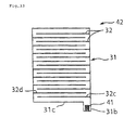
- a transparent antenna 42 shown in Fig. 33 has a rectangular antenna pattern 31 and slits 32 are formed on the antenna pattern 31.
- same symbols are assigned for the same components as those in Fig. 32 and their explanations will be omitted in the following description.
- a plurality of slits 32 are formed in parallel to the shorter side 31c of the antenna pattern 31 and among a plurality of the slits 32, slits 32c are formed with a slightly shorter length than the shorter side 31c from the right rim of the antenna pattern 31 and slits 32d are formed also with a slightly shorter length than the shorter side 31c from the left rim of the antenna pattern 31.
- the slits 32 are formed by alternately arranging the slits 32c and the slits 32d in the vertical direction and accordingly, the antenna pattern 31 snaking in the vertical direction is formed.
- a transparent antenna 43 shown in Fig. 34 has a rectangular antenna pattern 31 and provided with slits 32e extended in the vertical direction from the center of the tub 31b in the tub width direction, slits 32f branched in the transverse direction from the middle of the slits 32e, and a plurality of slits 32g and 32h formed slantingly in parallel state.
- the slits 32g are formed by cutting from the lower rim of the antenna pattern 31 and formed in a prescribed length without crossing the slits 32e and 32f
- the slits 32h are formed by cutting from the slits 32e or 32f and formed in a prescribed length without reaching the left rim 31d of the antenna pattern 31. Accordingly, the slantingly snaked antenna pattern 31 is formed within a range surrounded with the slits 32e and 32f.
- a transparent antenna 44 shown in Fig. 35 has a rectangular antenna pattern 31 and is provided with a slit 32i extended in a prescribed length from the center of the tub 31b in the tub width direction, a plurality slits 32j and 32j at right angles to the slit 32i, a slit 32k formed by cutting in a prescribed length from the left rim 31d of the antenna pattern 31, and a slit 32m formed by cutting in a prescribed length from the right rim 31e.
- antenna pattern 31 snaked in a left half and a right half of the antenna pattern 31 are formed while having the slit 32i as the boundary.
- a transparent antenna 45 shown in Fig. 36 has a rectangular antenna pattern 31 and the different point of the antenna pattern from that antenna pattern shown in Fig. 35 is that the slit 32n formed in place of the 32i is extended to the upper rim 31f of the antenna pattern 31.
- the antenna pattern 31 is divided right and left by the slit 32 n, these two antenna patterns 31, 31 are arranged adjacently and compose the transparent antenna.
- a housing component with an antenna according to the present invention is composed in a manner that it can be attached to a device without damaging a design provided on a housing of the device.
- the housing component with an antenna (hereinafter, abbreviated as housing component) 50 is composed of a resin plate 51 including a transparent window section 51a and an opaque decorative section 51b surrounding the transparent window section 51a in a frame form, and an antenna pattern as an electrically conductive section 1b formed on a surface of the opaque decorative section 51b.
- a symbol 1c denotes electrode part of the antenna pattern.
- the housing component is designed to constitute a part of TV display (including a table-top type) and a part of a housing of a mobile terminal device such as a mobile phone and the like.
- a surface cover 53 and a backside cover 54 becomes the housing component, but a window cover 53a alone can be called the housing component.
- each of a surface cover 56, an inner upper cover 57a, an inner lower cover 57b and a backside cover 58 becomes a housing component, but a window cover 57c of an inner surface side and a window cover 56a of a front surface side can also be called the housing component.
- Fig. 40 shows a T-T cut surface of Fig. 1, which will be explained taking an example of a window cover 53a as a housing component.
- a resin-molded plate 60 is formed in a shape of a desired housing component 50, and polycarbonate, acryl, polyethylene terephthalate, triacetyl cellulose and the like may be used as a material.
- a decorative layer 61 is to be provided on a front surface of the resin-molded plate 60 or a decorative layer 61 is provided on a backside surface of a resin-molded plate 60 as shown in Fig. 40(b) or (c).
- urethane resin As a material for the decorative layer 61, urethane resin, polycarbonate resin, vinyl resin, polyester resin and the like may be used. In particular, urethane-based resin is preferably used. Further, a colored ink containing a pigment or dye of a desired color may be used while using an elastomer of the urethane-based resin as a binder.
- a printing method such as offset printing, gravure printing, and screen printing and a coating method such as gravure coating, roll coating and comma coating may be employed.
- Transfer method and a simultaneous inmold transfer method may also be used.
- the transfer method comprises, using a transcription material formed with transcription layer composed of a separating layer, a decorative layer, an adhesive layer and the like on a base sheet, making the transfer layer adhere to the transcription object by applying heat and pressure, followed by separating the base sheet and transcribing the transfer layer alone on a surface of the transcription object for decoration.
- simultaneous inmold transfer method is a method comprising inserting a transcription material in a metal mold, injection-filling a cavity with a resin followed by cooling to obtain a molded resin piece, and simultaneously bonding a surface thereof with a transcription material followed by separating the base sheet, and transcribing a transfer layer on a surface of the transcription object.
- the base sheet may be kept without being separated, and in such a case, the separating layer may be omitted.
- a resin sheet such as polypropylene-based resin, polyethylene-based resin, polyamide-based resin, polyester-based resin, polyacrylic resin, and polyvinyl chloride-based resin may be used.
- a material of the separating layer in addition to a polyacrylic resin, a polyester-based resin, a polyvinyl chloride-based resin, a cellulose-based resin, a rubber-based resin, polyurethane-based resin, polyvinyl acetate-based resin and the like, a copolymer such as vinyl chloride-vinyl acetate copolymer-based resin, and ethylene-vinyl acetate copolymer-based resin may be used. If hardness is required for the separating layer, a photo-curing resin such as a ultraviolet thermosetting resin, a radiation curing resin such as an electron radiation curing resin, and a thermosetting resin may be selected.
- a photo-curing resin such as a ultraviolet thermosetting resin, a radiation curing resin such as an electron radiation curing resin, and a thermosetting resin may be selected.
- thermosensitive or a pressure sensitive resin suitable as a material for the transcription object is used as necessary.
- the material of the transcription object is a polyacrylic resin
- a polyacrylic resin may be used.
- the material of the transcription object is polyphenylene oxide copolymer polystyrene-based copolymer resin, a polycarbonate-based resin, styrene polystyrene-based blended resin, polyacrylic resin, polystyrene-based resin, polyamide-based resin and the like which has an affinity with the polystyrene-based blended resin may be used.
- a material of the transcription object is polypropylene resin
- chlorinated polyolefins resin chlorinated ethylene-vinyl acetate copolymer resin, cyclized rubber, and coumarone-indene resin can be used.
- the housing component with an antenna 50 shown in Fig. 37 is constituted as a window cover, it partially has the opaque decorative section 51b for the purpose of forming the transparent window section for display 51a, but an entire surface of the housing component with an antenna 50 may be the opaque decorative section 51b.
- a transparent window section 51a and a camera lens may be disposed, or, for other purposes, there may be a part in which an opaque decorative section 51b is not provided.
- Fig. 40 if an antenna pattern which is in a planar form and has a light transmission of 70 % or more is formed as the transparent antenna 50a on a front surface side of the layer which attaches the opaque decorative section 51b to the resin-molded plate 60 (refer to Figs. 40(a) to (d)), and the electrically conductive section 1b of the antenna pattern comprises an electrically conductive thin film of the mesh structure, and an outline of each mesh comprises an extra fine band having substantially an equal width, when looking at the opaque decorative section 51b, the antenna pattern is only recognized as a slight change of shading, so that the transparent antenna 50a does not damage a design added to the housing behind the transparent antenna 50a.
- the transparent antenna 50a since a relatively large area of the display can be used for the transparent antenna 50a, it can enhance receiver sensitivity and a good transmission and reception is achieved.
- the antenna pattern can be extended up to the transparent window section 51a (refer to Fig. 37).
- the electrically conductive thin film As the electrically conductive thin film, a metal thin film such as copper, nickel, aluminum, gold, and silver, or an electrically conductive resin paste film containing the these metal particulates or an electrically conductive resin paste film containing carbon particulates may be used.
- the electrically conductive thin film is formed into a fine mesh-shaped pattern by photo-etching or by an etching method using print resist or by a method printing an electrically conductive resin paste.
- the antenna pattern has an electrically conductive section 1c for power supply which is electrically connected with a mesh-shaped pattern.
- the antenna pattern is connected to the radio transmission section mounted in housing via a wiring.
- a housing component with an antenna 50 itself constitutes the window cover 53a and the rim portion is covered with an outer frame of another housing component with an antenna, it can be connected via an input-output terminal provided on an inner surface side of the outer frame.
- the antenna pattern may be formed directly on the resin-molded plate 60, or may be formed using a transcription method or simultaneous inmold transfer method in a same manner as the formation of the decorative layer 61. In a latter case, in the present embodiment, a base sheet may remain without being separated.
- the antenna pattern is the same as previously shown in Figs. 4 to 6.
- the transparent antenna 50a needs to be prevented from interfering with a mesh pattern constituting the picture element of the display so as not to form a moire pattern.
- a shape of a mesh aperture, pitch, and bias angle of the antenna pattern in the transparent antenna 50a is adjusted.
- an easy and convenient way is to make a few kinds of prototypes and check a presence of the moire pattern with eyes to determine the specification.
- Fig. 41 shows a first variation of the housing component with an antenna.
- a difference of the housing component with an antenna 65 shown by Fig. 41 from the housing component with an antenna 51 in Fig. 37 is that the opaque decorative section 51b is changed to the transmissive decorative section 66a.
- the housing component with an antenna 65 has a transmissive decorative section 66a in a part or an entire part of the resin-molded plate 66.
- the transmissive decorative section 66a causes a decorative effect by illuminating the resin-molded plate 66 from a back side thereof and an antenna pattern is formed on the transmissive decorative section 66a consists of the electrically conductive section 1b.
- the transmissive decorative section 66a emits light in various colors by illumination from the light source 67 positioned on a back side of the housing component 65 such as light-emitting diode and fluorescent light, and for example, taking an example of a cellular phone handset, the housing lights up in various colors in accordance with rhythms of ringing melody, game, and alarm which are accompanying functions of a cellular phone handset.
- the transmissive decorative section 66a can be obtained by forming the decorative layer 61, but decoration can be done by making the light-emitting diode and the fluorescent light which are positioned on the back side be colored in red, blue, green and the like, so the decorative layer 61 is not always necessary.
- a translucent decorative layer 61a needs to be provided on a front surface side or a backside of the resin-molded plate 60, or colorant needs to be included to a degree that translucency in a desired range in the resin-molded plate 60 can be obtained.
- the resin-molded plate 60 and the decorative layer 61 corresponding to the transmissive decorative section 66a can be any of colored transparent, half transparent, and opaque as long as it transmits light from the back side.
- a layer structure of the antenna pattern the resin-molded plate 60 or a layer structure adding the decorative layer 61 thereto transmits light via any layer of those from the back side unlike the above embodiment; thus, as shown by Fig. 42(b), the housing component with an antenna 65 may be positioned upside down so as to transmit light.
- the transmissive decorative section 66a and the transparent window section 51a are allowed to exist a part which is not decorated by illumination other than the transmissive decorative section 66a and the transparent window section 51a, such as in a case where a surrounding of the transparent window section 51a is rimmed with an opaque decorative section and the transmissive decorative section 66a is provided on the periphery of opaque decorative section.
- a light shielding layer may be formed on a necessary part of the front surface side or the backside of the resin-molded plate 60.
- a decorative layer containing a colorant to a degree that it can shield light may be formed.
- the housing component 68 shown in the figure is one in which a transparent decorative layer 61 is laminated on a resin-molded plate 69, and an electrically conductive section1b is formed on the decorative layer 61, and by illumination from the light source 67 positioned from a side of the housing component 68, the decorative layer 61 as a transmissive decorative section formed in a part or an entire part or an entire part on the resin-molded plate 69 has a decorative effect.
- a position of forming the antenna pattern comprising the electrically conductive section1b is limited to a front surface side of the resin-molded plate 69 because a method of illumination in the transmissive decorative section is different from that of the above-described first variation.
- a housing component is structured so that light is allowed to enter from a side of the resin-molded plate 69, and the light is introduced to a deeper side thereof by using an internal reflection effect of the resin-molded plate 69, and the incident light is reflected on a front surface side of the housing component 68 through a light output section 69a such as microscopic concavity and convexity and a reflection dot of a backside of the resin-molded plate 69, and thus it is meaningless to form the transparent antenna pattern and the decorative layer 61 having permeability on a backside of the resin-molded plate 69 which is not implicated in the decoration by illumination.
- a front surface of the electrically conductive section 1b of the antenna pattern can be covered with a transparent cover layer (transparent protection film).
- a transparent resin layer containing a plating catalyst was formed on a 100 ⁇ m-thick base sheet of a transparent polyethylene terephthalate film, and an electroless copper nickel plating was carried out, subsequently, copper electroplating were carried out to form a metal thin film.
- a mesh aperture was formed on the metal thin film (to be an electrically conductive thin film of the mesh structure) to give an antenna pattern having a light transmittance of 92 %.
- the electrically conductive section of the antenna pattern is a square mesh pattern as shown in Fig. 4, and an extra fine band thereof has a line width (w) of 15 ⁇ m, a pitch between lines of 400 ⁇ m and a bias angle of 30°.
- a decorative layer composed of any opaque pattern was formed on the part excluding the transparent window section for display and the electrode part of the antenna pattern to give an opaque decorative section.
- a cellular phone handset was assembled using the surface cover 53, and on the occasion, the electrode part 1c, exposed from the through hole of the molded resin material and a radio transmission section in the housing were connected using a wire.
- Example 18 It was same as Example 18 except that a light transmittance of the antenna pattern was 89 %, a shape of the mesh aperture of the electrically conductive section formed a regular hexagon lattice pattern of 500 ⁇ m on a side, and a line width of the extra fine metal band was 25 ⁇ m.
- Example 18 the step after forming the antenna pattern was changed to a following.
- a decorative layer composed of a light blocking pattern was provided on a rim section of the transparent window section for display in a frame-like form, a translucent decorative layer was formed on a transparent window section, a rim section thereof and a part of an antenna pattern excluding the electrode part to give a transmissive decorative section.
- red-color, blue-color and green-color light-emitting diodes were positioned on a backside of the transmissive decorative section of the surface cover 53. It was same as in Example 18 except for these changes.
- Example 19 microscopic concavity and convexity are provided on a back side of the resin-molded plate as a light output section, and red-color, blue-color and green-color light-emitting diodes were positioned on a side surface of the molded resin material instead of the back side of the transmissive decorative section of the surface cover 53. It was same as in Example 19 except for these changes.
- the housing component with an antenna is formed into a mesh structure in which an electrically conductive section of an antenna pattern has a number of apertures, and an outline of each mesh comprises extra fine bands, so that when an opaque decorative section and a transmissive decorative section are looked at, the antenna pattern is recognized only as a slight change of a shading, and the antenna pattern does not damage a design provided on a housing. Further, since a relatively large area on the display can be used as an area for positioning the antenna, receiver sensitivity can be improve and a good transmission and reception is made possible.
- a transparent antenna of the present invention can be used for receiving terrestrial broadcast and satellite broadcast by attaching the antenna to a front surface of a display of a mobile device such as a television monitor and a mobile phone.
Landscapes
- Engineering & Computer Science (AREA)
- Computer Networks & Wireless Communication (AREA)
- Details Of Aerials (AREA)
- Telephone Set Structure (AREA)
- Support Of Aerials (AREA)
Applications Claiming Priority (6)
| Application Number | Priority Date | Filing Date | Title |
|---|---|---|---|
| JP2005106529 | 2005-04-01 | ||
| JP2005127219 | 2005-04-25 | ||
| JP2005126895 | 2005-04-25 | ||
| JP2005155120 | 2005-05-27 | ||
| JP2005162002 | 2005-06-01 | ||
| PCT/JP2006/306957 WO2006106982A1 (fr) | 2005-04-01 | 2006-03-31 | Antenne transparente pour affichage, organe phototransmetteur pour affichage possedant une antenne, et element pour boitier, dote d’une antenne |
Publications (2)
| Publication Number | Publication Date |
|---|---|
| EP1868263A1 true EP1868263A1 (fr) | 2007-12-19 |
| EP1868263A4 EP1868263A4 (fr) | 2009-08-12 |
Family
ID=37073532
Family Applications (1)
| Application Number | Title | Priority Date | Filing Date |
|---|---|---|---|
| EP06730905A Withdrawn EP1868263A4 (fr) | 2005-04-01 | 2006-03-31 | Antenne transparente pour affichage, organe phototransmetteur pour affichage possedant une antenne, et element pour boitier, dote d une antenne |
Country Status (7)
| Country | Link |
|---|---|
| US (1) | US7847753B2 (fr) |
| EP (1) | EP1868263A4 (fr) |
| JP (1) | JP4814223B2 (fr) |
| KR (1) | KR101025054B1 (fr) |
| CN (1) | CN101180765B (fr) |
| TW (1) | TWI382590B (fr) |
| WO (1) | WO2006106982A1 (fr) |
Cited By (35)
| Publication number | Priority date | Publication date | Assignee | Title |
|---|---|---|---|---|
| GB2445434A (en) * | 2007-01-02 | 2008-07-09 | Samsung Electro Mech | Film antenna with a protective layer, mounted in or on the casing of a communication device |
| WO2009071124A1 (fr) * | 2007-12-06 | 2009-06-11 | Telefonaktiebolaget L M Ericsson (Publ) | Ensemble d'affichage |
| WO2009071127A1 (fr) * | 2007-12-06 | 2009-06-11 | Telefonaktiebolaget L M Ericsson (Publ) | Dispositif d'affichage et d'antenne combiné |
| EP2086048A1 (fr) * | 2008-01-30 | 2009-08-05 | Shenzhen Futaihong Precision Industry Co., Ltd. | Boîtier, dispositif de communication sans fil utilisant le boîtier et son procédé de fabrication |
| EP2086049A1 (fr) * | 2008-01-30 | 2009-08-05 | Shenzhen Futaihong Precision Industry Co., Ltd. | Boîtier, dispositif de communication sans fil utilisant le boîtier et son procédé de fabrication |
| EP2086050A1 (fr) * | 2008-01-30 | 2009-08-05 | Shenzhen Futaihong Precision Industry Co., Ltd. | Boîtier, dispositif de communication sans fil utilisant le boîtier et son procédé de fabrication |
| EP2096706A1 (fr) * | 2008-02-26 | 2009-09-02 | Shenzhen Futaihong Precision Industry Co., Ltd. | Boîtier, dispositif de communication sans fil utilisant le boîtier et son procédé de fabrication |
| EP2096707A1 (fr) * | 2008-02-26 | 2009-09-02 | Shenzhen Futaihong Precision Industry Co., Ltd. | Boîtier, dispositif de communication sans fil utilisant le boîtier et son procédé de fabrication |
| FR2936917A1 (fr) * | 2008-10-03 | 2010-04-09 | Affiliated Comp Services Solut | Terminal de communication sans contact a ecran |
| EP2246185A4 (fr) * | 2008-02-19 | 2011-05-18 | Nissha Printing | Grille et boîtier pour dispositifs électroniques |
| NL2007283C2 (en) * | 2010-08-27 | 2012-02-28 | Apple Inc | Antennas mounted under dielectric plates. |
| US8203491B2 (en) | 2008-01-30 | 2012-06-19 | Shenzhen Futaihong Precision Industry Co., Ltd. | Housing, wireless communication device using the housing, and manufacturing method thereof |
| EP2139010A4 (fr) * | 2007-04-16 | 2012-06-20 | Nissha Printing | Plaque mince transparente |
| EP2469642A1 (fr) * | 2010-12-22 | 2012-06-27 | Smart Approach Co., Ltd. | Module d'antenne, dispositif tactile et dispositif électronique doté de ceux-ci |
| US8712233B2 (en) | 2012-02-24 | 2014-04-29 | Apple Inc. | Electronic device assemblies |
| EP2369674A3 (fr) * | 2010-03-25 | 2014-07-02 | Sony Mobile Communications Japan, Inc. | Dispositif d'antenne et dispositif mobile |
| WO2015042335A1 (fr) * | 2013-09-23 | 2015-03-26 | Apple Inc. | Composant électronique intégré dans un matériau céramique |
| WO2015133842A1 (fr) | 2014-03-05 | 2015-09-11 | Samsung Electronics Co., Ltd. | Dispositif d'antenne et dispositif électronique comportant le dispositif d'antenne |
| EP2812779A4 (fr) * | 2012-02-10 | 2015-09-23 | 3M Innovative Properties Co | Structures de trames pour électrodes de capteur tactile |
| US9186828B2 (en) | 2012-06-06 | 2015-11-17 | Apple Inc. | Methods for forming elongated antennas with plastic support structures for electronic devices |
| US9318793B2 (en) | 2012-05-02 | 2016-04-19 | Apple Inc. | Corner bracket slot antennas |
| EP2402139A3 (fr) * | 2010-06-29 | 2016-04-20 | Lg Electronics Inc. | Boîtier de terminal mobile, terminal mobile en disposant et procédé de fabrication du terminal mobile |
| EP3041086A1 (fr) * | 2014-12-29 | 2016-07-06 | Samsung Electronics Co., Ltd. | Dispositif d'antenne et dispositif électronique comprenant celui-ci |
| EP3056978A1 (fr) * | 2009-02-26 | 2016-08-17 | 3M Innovative Properties Company | Capteur d'écran tactile et substrat à motifs comprenant des micro-motifs superposés à faible visibilité |
| US9455489B2 (en) | 2011-08-30 | 2016-09-27 | Apple Inc. | Cavity antennas |
| US9461357B2 (en) | 2014-02-12 | 2016-10-04 | Apple Inc. | Antenna on sapphire structure |
| WO2016186169A1 (fr) * | 2015-05-21 | 2016-11-24 | シャープ株式会社 | Dispositif d'affichage |
| EP1993164B1 (fr) * | 2007-05-17 | 2017-01-04 | Casio Computer Co., Ltd. | Antenne imprimée et équipement électronique |
| US9632537B2 (en) | 2013-09-23 | 2017-04-25 | Apple Inc. | Electronic component embedded in ceramic material |
| US9678540B2 (en) | 2013-09-23 | 2017-06-13 | Apple Inc. | Electronic component embedded in ceramic material |
| EP3114728A4 (fr) * | 2014-03-05 | 2017-10-25 | Samsung Electronics Co., Ltd. | Dispositif d'antenne et dispositif électronique comportant le dispositif d'antenne |
| FR3065119A1 (fr) * | 2017-04-10 | 2018-10-12 | Ingenico Group | Antenne configuree pour etre conformee a une surface transparente, dispositif d'affichage et dispositif de paiement electronique correspondants |
| EP4047741A4 (fr) * | 2019-11-20 | 2022-12-21 | Huawei Technologies Co., Ltd. | Plaque de couvercle et dispositif électronique |
| DE102010064225B4 (de) | 2010-12-28 | 2024-05-16 | Robert Bosch Gmbh | Vorrichtung aufweisend ein Display |
| EP4228249A4 (fr) * | 2020-10-08 | 2024-10-09 | Dai Nippon Printing Co., Ltd. | Visiocasque |
Families Citing this family (143)
| Publication number | Priority date | Publication date | Assignee | Title |
|---|---|---|---|---|
| EP1926221A4 (fr) * | 2005-09-12 | 2011-12-28 | Cell Cross Corp | Emetteur de signal |
| WO2008123191A1 (fr) * | 2007-03-30 | 2008-10-16 | Nissha Printing Co., Ltd. | Corps moulé en résine et son procédé de fabrication |
| JP5274801B2 (ja) * | 2007-08-30 | 2013-08-28 | 京セラ株式会社 | 携帯端末 |
| JP2009065388A (ja) * | 2007-09-05 | 2009-03-26 | Toshiba Corp | 無線装置及びアンテナ装置 |
| CN101889227B (zh) * | 2007-12-06 | 2014-12-10 | 爱立信电话股份有限公司 | 用于光表现和无线通信的设备 |
| JP5337814B2 (ja) * | 2007-12-06 | 2013-11-06 | テレフオンアクチーボラゲット エル エム エリクソン(パブル) | 機能拡張されたディスプレイ構成 |
| JP4190021B1 (ja) * | 2008-01-11 | 2008-12-03 | アサヒテック株式会社 | 導電性ボール配置用マスク及びその製造方法 |
| JP5109831B2 (ja) * | 2008-06-24 | 2012-12-26 | 住友電気工業株式会社 | アンテナユニット、灯器、交通信号灯器及び交通信号制御機 |
| KR101527988B1 (ko) * | 2008-06-27 | 2015-06-10 | 데이진 화이바 가부시키가이샤 | 통신용 시트 구조체 |
| US20100066613A1 (en) * | 2008-09-12 | 2010-03-18 | Sony Corporation | Antenna Device |
| US8325094B2 (en) * | 2009-06-17 | 2012-12-04 | Apple Inc. | Dielectric window antennas for electronic devices |
| KR20110027572A (ko) * | 2009-09-08 | 2011-03-16 | 한국전자통신연구원 | 근접장을 이용하는 통신 장치 |
| US20110059692A1 (en) * | 2009-09-08 | 2011-03-10 | Electronics And Telecommunications Research Institute | Communications device using near field |
| JP5549165B2 (ja) * | 2009-09-17 | 2014-07-16 | 大日本印刷株式会社 | 透明アンテナ及び該透明アンテナの製造方法 |
| JP5414451B2 (ja) * | 2009-10-21 | 2014-02-12 | パナソニック株式会社 | アンテナ装置 |
| KR101610207B1 (ko) * | 2010-01-07 | 2016-04-07 | 엘지전자 주식회사 | 이동 단말기 |
| CN102195125A (zh) * | 2010-03-03 | 2011-09-21 | 深圳富泰宏精密工业有限公司 | 多频天线 |
| CN202217782U (zh) * | 2010-05-24 | 2012-05-09 | Tdk株式会社 | 接近型天线以及无线通信设备 |
| US7992773B1 (en) * | 2010-09-15 | 2011-08-09 | Reagan Inventions, Llc | System and method for presenting information about an object on a portable electronic device |
| KR20140030120A (ko) | 2010-12-16 | 2014-03-11 | 쓰리엠 이노베이티브 프로퍼티즈 컴파니 | 투명한 미세 패턴화된 rfid 안테나 및 이를 포함하는 물품 |
| KR20120072220A (ko) * | 2010-12-23 | 2012-07-03 | 한국전자통신연구원 | 터치입력장치 및 이를 이용한 전자기파 송수신 장치 |
| JP5657421B2 (ja) * | 2011-02-17 | 2015-01-21 | 三菱電線工業株式会社 | アンテナ |
| JP5682464B2 (ja) * | 2011-06-13 | 2015-03-11 | 大日本印刷株式会社 | 透明アンテナ、及び画像表示装置 |
| CN102983391B (zh) | 2011-09-06 | 2016-09-07 | 数伦计算机技术(上海)有限公司 | 一种高光通透性天线 |
| KR20130037948A (ko) * | 2011-10-07 | 2013-04-17 | 한국전자통신연구원 | 전자파 저감 투명 필름의 제조 방법 및 전자파 저감 투명 필름 |
| JP5875484B2 (ja) | 2011-12-22 | 2016-03-02 | 富士フイルム株式会社 | 導電シート及びタッチパネル |
| CN103179815A (zh) * | 2011-12-24 | 2013-06-26 | 富泰华工业(深圳)有限公司 | 电子装置壳体 |
| TW201332211A (zh) * | 2012-01-24 | 2013-08-01 | Taiwan Green Point Entpr Co | 感應式電子裝置的製作方法 |
| KR101916241B1 (ko) * | 2012-03-12 | 2018-11-07 | 삼성전자주식회사 | 휴대용 단말기의 안테나 장치 |
| KR101859575B1 (ko) * | 2012-03-21 | 2018-05-18 | 삼성전자 주식회사 | 근거리무선통신 안테나 장치 및 이를 구비하는 전자기기 |
| JP5779535B2 (ja) * | 2012-03-30 | 2015-09-16 | 富士フイルム株式会社 | 導電性フイルム、それを備える表示装置及び導電性フイルムのパターンの決定方法 |
| US9059514B2 (en) | 2012-05-29 | 2015-06-16 | Apple Inc. | Structures for shielding and mounting components in electronic devices |
| KR20140000549A (ko) * | 2012-06-25 | 2014-01-03 | 삼성전자주식회사 | 하우징 가공 방법 및 장치 |
| US8831537B2 (en) | 2012-08-13 | 2014-09-09 | Lsi Corporation | Transitory touchscreen antenna structure |
| EP2921464B1 (fr) | 2012-11-14 | 2020-12-30 | Sekisui Chemical Co., Ltd. | Intercalaire pour verre feuilleté et verre feuilleté |
| US8941095B2 (en) | 2012-12-06 | 2015-01-27 | Hrl Laboratories, Llc | Methods for integrating and forming optically transparent devices on surfaces |
| CN103857172A (zh) * | 2012-12-06 | 2014-06-11 | 富葵精密组件(深圳)有限公司 | 透明印刷电路板 |
| US9099790B2 (en) * | 2012-12-27 | 2015-08-04 | Htc Corporation | Mobile device and antenna structure therein |
| US20150029067A1 (en) * | 2013-03-13 | 2015-01-29 | Aliphcom | Rf signal pickup from an electrically conductive substrate utilizing passive slits |
| US9594454B2 (en) * | 2013-03-29 | 2017-03-14 | Sharp Kabushiki Kaisha | Touch-panel substrate and electronic device |
| US9634383B2 (en) * | 2013-06-26 | 2017-04-25 | Pulse Finland Oy | Galvanically separated non-interacting antenna sector apparatus and methods |
| KR101399835B1 (ko) * | 2013-07-09 | 2014-05-27 | 박상인 | 무선통신기기 케이스의 제조방법 및 이 방법에 의해 제조된 무선통신기기 케이스 |
| CN104577304B (zh) * | 2013-10-18 | 2019-07-23 | 深圳富泰宏精密工业有限公司 | 天线结构及具有该天线结构的无线通信装置 |
| KR102045113B1 (ko) * | 2013-11-01 | 2019-11-14 | 피피지 인더스트리즈 오하이오 인코포레이티드 | 전기전도성 물질의 전달 방법 |
| JP6208577B2 (ja) | 2013-12-24 | 2017-10-04 | 京セラ株式会社 | 携帯端末 |
| US9582470B2 (en) * | 2014-01-10 | 2017-02-28 | Christopher Sterling | Antenna apparatus and software for emulating same |
| US20150295326A1 (en) * | 2014-01-10 | 2015-10-15 | Christopher Sterling | Antenna apparatus and software for emulating same |
| KR101849149B1 (ko) * | 2014-01-16 | 2018-04-16 | 미쓰비시 세이시 가부시키가이샤 | 광투과성 도전재료 |
| US10074893B2 (en) * | 2014-02-10 | 2018-09-11 | Srihitha Shopping Services Pvt. Ltd | Device used to reduce electromagnetic radiations |
| US9547335B1 (en) | 2014-03-31 | 2017-01-17 | Google Inc. | Transparent module antenna for wearable devices |
| CN105449347A (zh) * | 2014-05-30 | 2016-03-30 | 联想(北京)有限公司 | 一种天线以及通讯电子设备 |
| KR102154325B1 (ko) * | 2014-07-04 | 2020-09-09 | 삼성전자주식회사 | 안테나 및 이를 구비한 모바일 장치 |
| EP2992776B1 (fr) * | 2014-09-04 | 2019-11-06 | WITS Co., Ltd. | Boîtier et appareil le comprenant |
| KR102139217B1 (ko) * | 2014-09-25 | 2020-07-29 | 삼성전자주식회사 | 안테나 장치 |
| KR102175750B1 (ko) * | 2014-10-29 | 2020-11-06 | 삼성전자주식회사 | 안테나 장치 및 이를 구비하는 전자 장치 |
| US9870493B2 (en) | 2014-11-25 | 2018-01-16 | Sharp Kabushiki Kaisha | Antenna loop configuration for more efficiently surrounding the high intensity area of the magnetic field produced by an IC card |
| WO2016098761A1 (fr) * | 2014-12-18 | 2016-06-23 | シャープ株式会社 | Antenne transparente et dispositif d'affichage à antenne transparente |
| CN107004956B (zh) | 2014-12-18 | 2019-12-27 | 夏普株式会社 | 透明天线及附透明天线的显示装置 |
| JP6413022B2 (ja) * | 2014-12-26 | 2018-10-24 | ビーワイディー カンパニー リミテッド | 通信機器の金属シェル |
| USD759885S1 (en) * | 2015-02-16 | 2016-06-21 | Taeg Kim Nishimoto | Hexagonal translucent mesh light source container |
| US10551949B2 (en) * | 2015-05-08 | 2020-02-04 | Intel Corporation | Display integrated antenna |
| JP6421077B2 (ja) | 2015-05-19 | 2018-11-07 | 富士フイルム株式会社 | アンテナの製造方法およびタッチセンサ |
| CN112436045B (zh) | 2015-05-27 | 2023-12-19 | 三星电子株式会社 | 显示装置 |
| US10401548B2 (en) * | 2015-09-24 | 2019-09-03 | Intel Corporation | Integrated antenna with display uniformity |
| KR102443196B1 (ko) | 2015-09-25 | 2022-09-15 | 삼성전자주식회사 | 전자 장치 |
| KR102406686B1 (ko) * | 2015-11-10 | 2022-06-08 | 삼성전자주식회사 | 안테나 장치 및 그를 구비하는 전자 장치 |
| CN109075446B (zh) * | 2016-01-29 | 2020-09-08 | 夏普株式会社 | 天线设备 |
| JP6761591B2 (ja) * | 2016-03-25 | 2020-09-30 | 大日本印刷株式会社 | アンテナ |
| KR102469566B1 (ko) | 2016-03-31 | 2022-11-22 | 삼성전자주식회사 | 안테나 장치를 포함하는 전자 장치 |
| ES2794899T3 (es) | 2016-05-02 | 2020-11-19 | Samsung Electronics Co Ltd | Procedimiento de visualización de pantalla y dispositivo electrónico que soporta la misma |
| US10634313B2 (en) | 2016-06-08 | 2020-04-28 | Sharp Kabushiki Kaisha | Light-emitting device, authentication notification system, and door |
| KR102666192B1 (ko) * | 2016-07-28 | 2024-05-14 | 삼성디스플레이 주식회사 | 표시 장치 |
| US10367252B2 (en) * | 2016-08-11 | 2019-07-30 | Apple Inc. | Broadband antenna |
| CN109661752A (zh) * | 2016-09-23 | 2019-04-19 | 富士胶片株式会社 | 移动通信终端 |
| KR102264790B1 (ko) * | 2016-12-20 | 2021-06-15 | 한국전자기술연구원 | 신축성 있는 안테나 소자 |
| CN108270070A (zh) * | 2017-01-03 | 2018-07-10 | 中兴通讯股份有限公司 | 一种液态天线结构及其控制方法 |
| KR102035689B1 (ko) * | 2017-02-23 | 2019-10-23 | 동우 화인켐 주식회사 | 필름형 안테나 및 이를 포함하는 화상 표시 장치 |
| KR102188997B1 (ko) * | 2017-02-28 | 2020-12-09 | 동우 화인켐 주식회사 | 투명 필름 안테나 |
| CN108539386B (zh) * | 2017-03-01 | 2020-02-21 | 华为技术有限公司 | 一种天线结构及无线终端 |
| KR102009382B1 (ko) | 2017-03-03 | 2019-08-09 | 동우 화인켐 주식회사 | 안테나가 구비된 터치 센서 |
| JP6809499B2 (ja) * | 2017-04-04 | 2021-01-06 | 株式会社Soken | 光透過型アンテナ、窓部貼付型通信モジュール、及び、周辺監視ユニット |
| JP6325719B1 (ja) * | 2017-05-31 | 2018-05-16 | 日本航空電子工業株式会社 | ループアンテナ |
| US10305163B2 (en) * | 2017-08-14 | 2019-05-28 | GM Global Technology Operations LLC | Method and apparatus for semitransparent antenna and transmission lines |
| KR102158204B1 (ko) | 2017-08-24 | 2020-09-22 | 동우 화인켐 주식회사 | 필름 안테나 및 이를 포함하는 디스플레이 장치 |
| TWI653781B (zh) * | 2017-09-01 | 2019-03-11 | 巨擘科技股份有限公司 | 行動裝置 |
| US10249944B1 (en) * | 2017-09-25 | 2019-04-02 | Antwave Intellectual Property Limited | Systems, apparatus, and methods to improve antenna performance in electronic devices |
| US10847887B2 (en) * | 2017-10-05 | 2020-11-24 | Eastman Kodak Company | Method for fabricating a transparent antenna |
| WO2019088792A1 (fr) * | 2017-11-06 | 2019-05-09 | 동우화인켐 주식회사 | Antenne à film et dispositif d'affichage comprenant celle-ci |
| KR101973742B1 (ko) * | 2018-01-18 | 2019-04-29 | 동우 화인켐 주식회사 | 필름 안테나 및 이를 포함하는 디스플레이 장치 |
| KR101967771B1 (ko) * | 2017-11-06 | 2019-04-10 | 동우 화인켐 주식회사 | 필름 안테나 및 이를 포함하는 디스플레이 장치 |
| TWI905068B (zh) * | 2017-11-29 | 2025-11-11 | 日商大日本印刷股份有限公司 | 配線基板 |
| EP3682504A4 (fr) | 2017-12-08 | 2021-04-28 | Hewlett-Packard Development Company, L.P. | Bandes antennes flexibles |
| CN112771722B (zh) * | 2018-09-28 | 2024-06-25 | 大日本印刷株式会社 | 配线基板和配线基板的制造方法 |
| WO2020071316A1 (fr) * | 2018-10-03 | 2020-04-09 | Agc株式会社 | Antenne planaire et vitre de fenêtre |
| KR101971490B1 (ko) * | 2018-10-16 | 2019-04-23 | 동우 화인켐 주식회사 | 필름 안테나 및 이를 포함하는 디스플레이 장치 |
| KR102455588B1 (ko) * | 2018-12-06 | 2022-10-14 | 동우 화인켐 주식회사 | 안테나 구조체 및 이를 포함하는 디스플레이 장치 |
| CN114204255A (zh) | 2019-01-09 | 2022-03-18 | 华为技术有限公司 | 一种终端设备 |
| KR102233687B1 (ko) | 2019-04-19 | 2021-03-29 | 동우 화인켐 주식회사 | 안테나 소자 및 이를 포함하는 디스플레이 장치 |
| WO2020227280A1 (fr) | 2019-05-06 | 2020-11-12 | 3M Innovative Properties Company | Article à motifs comprenant des éléments conducteurs de l'électricité |
| CN113939956A (zh) | 2019-06-12 | 2022-01-14 | 3M创新有限公司 | 透明天线叠堆和组件 |
| KR102832891B1 (ko) * | 2019-07-22 | 2025-07-11 | 코닝 인코포레이티드 | 밀리 미터 파(mili meter Wave, mmW) 반사 구조, mmW 반사 지향 구조 및 mmW 투과 구조 |
| CN110519953A (zh) * | 2019-07-27 | 2019-11-29 | 南昌欧菲光科技有限公司 | 电子设备及其盖板 |
| CN110519954B (zh) * | 2019-07-27 | 2024-12-03 | 安徽精卓光显技术有限责任公司 | 电子设备及其盖板 |
| EP4004817A1 (fr) * | 2019-07-31 | 2022-06-01 | Avery Dennison Retail Information Services, LLC | Dispositifs rfid à propriétés optiques contrôlées |
| US11955708B2 (en) | 2019-08-22 | 2024-04-09 | Lg Electronics Inc. | Electronic device equipped with transparent antenna |
| WO2021033805A1 (fr) * | 2019-08-22 | 2021-02-25 | 엘지전자 주식회사 | Dispositif électronique ayant une antenne transparente |
| EP3787190A1 (fr) | 2019-08-27 | 2021-03-03 | The Swatch Group Research and Development Ltd | Antenne pour communication en champ proche |
| TWI708430B (zh) * | 2019-10-02 | 2020-10-21 | 友達光電股份有限公司 | 透明天線及電子裝置 |
| KR102663550B1 (ko) * | 2019-10-30 | 2024-05-09 | 삼성전자 주식회사 | 안테나 모듈을 포함하는 전자 장치 |
| KR102805061B1 (ko) | 2019-10-31 | 2025-05-12 | 삼성디스플레이 주식회사 | 표시 장치 |
| KR102756487B1 (ko) | 2019-10-31 | 2025-01-21 | 삼성디스플레이 주식회사 | 무선 주파수 소자 및 이를 포함하는 전자 장치 |
| KR20210052749A (ko) | 2019-10-31 | 2021-05-11 | 삼성디스플레이 주식회사 | 표시 장치 및 이를 포함하는 전가 기기 |
| WO2021112286A1 (fr) * | 2019-12-05 | 2021-06-10 | 엘지전자 주식회사 | Dispositif électronique ayant une antenne transparente |
| KR102241964B1 (ko) * | 2019-12-05 | 2021-04-16 | 동우 화인켐 주식회사 | 안테나 소자 및 이를 포함하는 디스플레이 장치 |
| CN210984952U (zh) | 2019-12-06 | 2020-07-10 | 昇印光电(昆山)股份有限公司 | 一种透明天线 |
| KR102292322B1 (ko) * | 2020-02-16 | 2021-08-24 | 크리모 주식회사 | 방사체 모듈 및 그 제어 방법, 안테나 장치 및 모바일 디바이스 |
| CN111342229A (zh) * | 2020-03-27 | 2020-06-26 | 安徽精卓光显技术有限责任公司 | 后壳及电子设备 |
| WO2021229994A1 (fr) * | 2020-05-13 | 2021-11-18 | 富士フイルム株式会社 | Antenne |
| CN111564692B (zh) | 2020-05-20 | 2021-09-07 | 维沃移动通信有限公司 | 电子设备 |
| US12573766B2 (en) | 2020-06-16 | 2026-03-10 | 3M Innovative Properties Company | Patterned article including metallic bodies |
| KR20210158490A (ko) * | 2020-06-24 | 2021-12-31 | 동우 화인켐 주식회사 | 안테나 소자 및 이를 포함하는 디스플레이 장치 |
| CN111584990B (zh) * | 2020-06-30 | 2024-07-16 | 江西创新科技有限公司 | 带led可变色电视天线 |
| JP2022029727A (ja) * | 2020-08-05 | 2022-02-18 | 三菱電機株式会社 | アンテナ内蔵タッチスクリーンおよび表示装置 |
| KR102832198B1 (ko) * | 2020-09-24 | 2025-07-09 | 삼성전자주식회사 | 안테나를 포함하는 전자 장치 |
| CN112164871B (zh) * | 2020-09-28 | 2024-04-16 | 京东方科技集团股份有限公司 | 天线及其制备方法、电子装置 |
| JP7528717B2 (ja) * | 2020-10-28 | 2024-08-06 | 大日本印刷株式会社 | 配線基板および配線基板の製造方法 |
| TWI774206B (zh) * | 2021-01-22 | 2022-08-11 | 啟碁科技股份有限公司 | 天線裝置 |
| CN114976605B (zh) * | 2021-02-23 | 2024-01-30 | 北京京东方技术开发有限公司 | 薄膜传感器、薄膜传感器阵列及电子装置 |
| JPWO2022196730A1 (fr) * | 2021-03-16 | 2022-09-22 | ||
| KR102930627B1 (ko) * | 2021-03-24 | 2026-02-26 | 동우 화인켐 주식회사 | 안테나 소자 및 이를 포함하는 디스플레이 장치 |
| CN113067141B (zh) * | 2021-04-02 | 2022-12-20 | 京东方科技集团股份有限公司 | 一种薄膜天线、显示模组及显示装置 |
| WO2022216806A1 (fr) * | 2021-04-09 | 2022-10-13 | American University Of Beirut | Antenne reconfigurable mécaniquement basée sur des motifs de moiré et procédés d'utilisation de celle-ci |
| USD947820S1 (en) * | 2021-04-21 | 2022-04-05 | Shenzhen TUKO Technology Co., Ltd | Digital TV antenna |
| CN115552728B (zh) | 2021-04-29 | 2025-04-18 | 京东方科技集团股份有限公司 | 天线及其制备方法、天线系统 |
| TWI818257B (zh) * | 2021-05-07 | 2023-10-11 | 財團法人工業技術研究院 | 透明天線及其製作方法 |
| KR20240034781A (ko) * | 2021-07-12 | 2024-03-14 | 엘지전자 주식회사 | 안테나 장치 및 이를 구비하는 영상표시장치 |
| CN115642387A (zh) | 2021-07-20 | 2023-01-24 | 北京京东方技术开发有限公司 | 天线及天线系统 |
| DE102021128147A1 (de) | 2021-10-28 | 2023-05-04 | Audi Ag | Antennenvorrichtung für ein Kraftfahrzeug, Radarvorrichtung, Kommunikationsvorrichtung, Assistenzsystem sowie Verfahren |
| US20250194361A1 (en) * | 2022-04-13 | 2025-06-12 | Dai Nippon Printing Co., Ltd. | Wiring board, module, and image display device |
| US12614832B1 (en) * | 2022-09-23 | 2026-04-28 | Meta Platforms Technologies, Llc | Transparent antenna system for reducing visual artifacts |
| TW202416581A (zh) | 2022-10-07 | 2024-04-16 | 財團法人工業技術研究院 | 透光天線 |
| US12311637B2 (en) | 2022-11-04 | 2025-05-27 | Agc Automotive Americas Co. | Laminated glazing assembly including an antenna assembly |
| US12444827B2 (en) | 2023-03-02 | 2025-10-14 | King Fahd University Of Petroleum And Minerals | Transparent MIMO antenna for closely spaced antenna elements |
Family Cites Families (26)
| Publication number | Priority date | Publication date | Assignee | Title |
|---|---|---|---|---|
| JPS6449302A (en) * | 1987-08-19 | 1989-02-23 | Dainippon Printing Co Ltd | Film antenna |
| JP2537658Y2 (ja) | 1987-09-17 | 1997-06-04 | 三菱マテリアル株式会社 | 圧延ロール |
| JPH02256304A (ja) * | 1989-03-29 | 1990-10-17 | Honda Denshi Giken:Kk | 透明平面アンテナおよびそれを利用した通信システム |
| JPH0339911A (ja) | 1989-04-14 | 1991-02-20 | Sumitomo Electric Ind Ltd | 多心光ファイバ心線の分岐部 |
| US6268832B1 (en) * | 1994-09-28 | 2001-07-31 | Bsh Industries Limited | Radio antenna for vehicle window |
| JP3490304B2 (ja) * | 1997-10-17 | 2004-01-26 | シャープ株式会社 | 無線通信装置 |
| US6384790B2 (en) * | 1998-06-15 | 2002-05-07 | Ppg Industries Ohio, Inc. | Antenna on-glass |
| JP2000138512A (ja) * | 1998-09-23 | 2000-05-16 | Sharp Corp | 平面アンテナを備えた液晶表示装置 |
| JP2000124730A (ja) * | 1998-10-19 | 2000-04-28 | Dx Antenna Co Ltd | Vhf/uhf帯フィルムアンテナ |
| JP3594224B2 (ja) | 1999-05-28 | 2004-11-24 | 富士通テン株式会社 | フィルムアンテナ |
| JP2001196826A (ja) | 2000-01-14 | 2001-07-19 | Nippon Sheet Glass Co Ltd | 住居窓ガラス用フィルムアンテナ |
| JP3651349B2 (ja) * | 2000-03-23 | 2005-05-25 | 日本板硝子株式会社 | フィルムアンテナ装置 |
| CN1384561A (zh) * | 2001-05-08 | 2002-12-11 | 中华映管股份有限公司 | 无线移动通讯终端机透明天线及其制作方法 |
| JP2003090903A (ja) * | 2001-06-18 | 2003-03-28 | Shuho:Kk | 透過可視性フィルタ |
| US6538620B2 (en) * | 2001-07-09 | 2003-03-25 | Susan Lin | Safe sticker antenna for mobile phones |
| US6933891B2 (en) * | 2002-01-29 | 2005-08-23 | Calamp Corp. | High-efficiency transparent microwave antennas |
| JP2003258483A (ja) | 2002-02-28 | 2003-09-12 | Toppan Printing Co Ltd | 電磁波シールド転写材及び電磁波シールド材 |
| DE10314094A1 (de) | 2002-09-17 | 2004-03-25 | Pilkington Automotive Deutschland Gmbh | Antennenscheibe |
| JP4101637B2 (ja) | 2002-12-24 | 2008-06-18 | シャープ株式会社 | 携帯電話端末 |
| JP2004289393A (ja) * | 2003-03-20 | 2004-10-14 | Nippon Antenna Co Ltd | 広告掲示板 |
| US6862002B2 (en) * | 2003-05-28 | 2005-03-01 | Motorola, Inc. | Antenna ground plane and wireless communication device with antenna ground plane and acoustic resistor |
| JP2004356823A (ja) | 2003-05-28 | 2004-12-16 | Nec Corp | 携帯端末 |
| EP1486895A1 (fr) | 2003-06-13 | 2004-12-15 | Sap Ag | Système et procédé informatiques pour créer des notes de frais de voyage |
| JP2005064174A (ja) * | 2003-08-11 | 2005-03-10 | Shin Etsu Polymer Co Ltd | 電磁波シールド体及びその製造方法 |
| JP2005142984A (ja) * | 2003-11-10 | 2005-06-02 | Shin Etsu Polymer Co Ltd | 透光性アンテナ |
| JP4672389B2 (ja) * | 2005-02-24 | 2011-04-20 | 富士通株式会社 | アンテナ装置 |
-
2006
- 2006-03-31 CN CN2006800175692A patent/CN101180765B/zh not_active Expired - Fee Related
- 2006-03-31 EP EP06730905A patent/EP1868263A4/fr not_active Withdrawn
- 2006-03-31 US US11/887,579 patent/US7847753B2/en not_active Expired - Fee Related
- 2006-03-31 KR KR1020077025223A patent/KR101025054B1/ko not_active Expired - Fee Related
- 2006-03-31 TW TW095111635A patent/TWI382590B/zh not_active IP Right Cessation
- 2006-03-31 JP JP2007511212A patent/JP4814223B2/ja not_active Expired - Fee Related
- 2006-03-31 WO PCT/JP2006/306957 patent/WO2006106982A1/fr not_active Ceased
Cited By (56)
| Publication number | Priority date | Publication date | Assignee | Title |
|---|---|---|---|---|
| GB2445434B (en) * | 2007-01-02 | 2011-10-12 | Samsung Electro Mech | Film type antenna and mobile communication terminal case using the same |
| US7548206B2 (en) | 2007-01-02 | 2009-06-16 | Samsung Electro-Mechanics Co., Ltd. | Film type antenna and mobile communication terminal case using the same |
| GB2445434A (en) * | 2007-01-02 | 2008-07-09 | Samsung Electro Mech | Film antenna with a protective layer, mounted in or on the casing of a communication device |
| EP2139010A4 (fr) * | 2007-04-16 | 2012-06-20 | Nissha Printing | Plaque mince transparente |
| US8692130B2 (en) | 2007-04-16 | 2014-04-08 | Nissha Printing Co., Ltd. | Transparent thin plate |
| EP1993164B1 (fr) * | 2007-05-17 | 2017-01-04 | Casio Computer Co., Ltd. | Antenne imprimée et équipement électronique |
| US8213757B2 (en) | 2007-12-06 | 2012-07-03 | Telefonaktiebolaget L M Ericsson (Publ) | Combined display and antenna arrangement |
| WO2009071127A1 (fr) * | 2007-12-06 | 2009-06-11 | Telefonaktiebolaget L M Ericsson (Publ) | Dispositif d'affichage et d'antenne combiné |
| WO2009071124A1 (fr) * | 2007-12-06 | 2009-06-11 | Telefonaktiebolaget L M Ericsson (Publ) | Ensemble d'affichage |
| EP2086049A1 (fr) * | 2008-01-30 | 2009-08-05 | Shenzhen Futaihong Precision Industry Co., Ltd. | Boîtier, dispositif de communication sans fil utilisant le boîtier et son procédé de fabrication |
| EP2086050A1 (fr) * | 2008-01-30 | 2009-08-05 | Shenzhen Futaihong Precision Industry Co., Ltd. | Boîtier, dispositif de communication sans fil utilisant le boîtier et son procédé de fabrication |
| US8203491B2 (en) | 2008-01-30 | 2012-06-19 | Shenzhen Futaihong Precision Industry Co., Ltd. | Housing, wireless communication device using the housing, and manufacturing method thereof |
| EP2086048A1 (fr) * | 2008-01-30 | 2009-08-05 | Shenzhen Futaihong Precision Industry Co., Ltd. | Boîtier, dispositif de communication sans fil utilisant le boîtier et son procédé de fabrication |
| CN103252940B (zh) * | 2008-02-19 | 2015-04-01 | 日本写真印刷株式会社 | 网状片 |
| US8003900B2 (en) | 2008-02-19 | 2011-08-23 | Nissha Printing Co., Ltd. | Mesh sheet and housing for electronic devices |
| EP2246185A4 (fr) * | 2008-02-19 | 2011-05-18 | Nissha Printing | Grille et boîtier pour dispositifs électroniques |
| CN103252940A (zh) * | 2008-02-19 | 2013-08-21 | 日本写真印刷株式会社 | 网状片 |
| KR101154146B1 (ko) * | 2008-02-19 | 2012-06-14 | 니폰샤신인사츠가부시키가이샤 | 메쉬 시트 및 전자기기의 덮개 부품 |
| EP2096707A1 (fr) * | 2008-02-26 | 2009-09-02 | Shenzhen Futaihong Precision Industry Co., Ltd. | Boîtier, dispositif de communication sans fil utilisant le boîtier et son procédé de fabrication |
| EP2096706A1 (fr) * | 2008-02-26 | 2009-09-02 | Shenzhen Futaihong Precision Industry Co., Ltd. | Boîtier, dispositif de communication sans fil utilisant le boîtier et son procédé de fabrication |
| FR2936917A1 (fr) * | 2008-10-03 | 2010-04-09 | Affiliated Comp Services Solut | Terminal de communication sans contact a ecran |
| EP3056978A1 (fr) * | 2009-02-26 | 2016-08-17 | 3M Innovative Properties Company | Capteur d'écran tactile et substrat à motifs comprenant des micro-motifs superposés à faible visibilité |
| EP2369674A3 (fr) * | 2010-03-25 | 2014-07-02 | Sony Mobile Communications Japan, Inc. | Dispositif d'antenne et dispositif mobile |
| EP2402139A3 (fr) * | 2010-06-29 | 2016-04-20 | Lg Electronics Inc. | Boîtier de terminal mobile, terminal mobile en disposant et procédé de fabrication du terminal mobile |
| US8766858B2 (en) | 2010-08-27 | 2014-07-01 | Apple Inc. | Antennas mounted under dielectric plates |
| US9577315B2 (en) | 2010-08-27 | 2017-02-21 | Apple Inc. | Antennas mounted under dielectric plates |
| NL2007283C2 (en) * | 2010-08-27 | 2012-02-28 | Apple Inc | Antennas mounted under dielectric plates. |
| EP2424034A1 (fr) * | 2010-08-27 | 2012-02-29 | Apple Inc. | Antennes montées sous des plaques diélectriques |
| EP2469642A1 (fr) * | 2010-12-22 | 2012-06-27 | Smart Approach Co., Ltd. | Module d'antenne, dispositif tactile et dispositif électronique doté de ceux-ci |
| DE102010064225B4 (de) | 2010-12-28 | 2024-05-16 | Robert Bosch Gmbh | Vorrichtung aufweisend ein Display |
| US9455489B2 (en) | 2011-08-30 | 2016-09-27 | Apple Inc. | Cavity antennas |
| US10430001B2 (en) | 2012-02-10 | 2019-10-01 | 3M Innovative Properties Company | Mesh patterns for touch sensor electrodes |
| US9639228B2 (en) | 2012-02-10 | 2017-05-02 | 3M Innovative Properties Company | Mesh patterns for touch sensor electrodes |
| EP2812779A4 (fr) * | 2012-02-10 | 2015-09-23 | 3M Innovative Properties Co | Structures de trames pour électrodes de capteur tactile |
| US9360971B2 (en) | 2012-02-10 | 2016-06-07 | 3M Innovative Properties Company | Mesh patterns for touch sensor electrodes |
| US9137891B2 (en) | 2012-02-24 | 2015-09-15 | Apple Inc. | Electronic device assemblies |
| US8712233B2 (en) | 2012-02-24 | 2014-04-29 | Apple Inc. | Electronic device assemblies |
| US9318793B2 (en) | 2012-05-02 | 2016-04-19 | Apple Inc. | Corner bracket slot antennas |
| US9186828B2 (en) | 2012-06-06 | 2015-11-17 | Apple Inc. | Methods for forming elongated antennas with plastic support structures for electronic devices |
| WO2015042335A1 (fr) * | 2013-09-23 | 2015-03-26 | Apple Inc. | Composant électronique intégré dans un matériau céramique |
| US9632537B2 (en) | 2013-09-23 | 2017-04-25 | Apple Inc. | Electronic component embedded in ceramic material |
| US9678540B2 (en) | 2013-09-23 | 2017-06-13 | Apple Inc. | Electronic component embedded in ceramic material |
| US9461357B2 (en) | 2014-02-12 | 2016-10-04 | Apple Inc. | Antenna on sapphire structure |
| US9692113B2 (en) | 2014-02-12 | 2017-06-27 | Apple Inc. | Antenna on sapphire structure |
| WO2015133842A1 (fr) | 2014-03-05 | 2015-09-11 | Samsung Electronics Co., Ltd. | Dispositif d'antenne et dispositif électronique comportant le dispositif d'antenne |
| EP3114728A4 (fr) * | 2014-03-05 | 2017-10-25 | Samsung Electronics Co., Ltd. | Dispositif d'antenne et dispositif électronique comportant le dispositif d'antenne |
| US10622703B2 (en) | 2014-03-05 | 2020-04-14 | Samsung Electronics Co., Ltd | Antenna device and electronic device having the antenna device |
| EP3041086A1 (fr) * | 2014-12-29 | 2016-07-06 | Samsung Electronics Co., Ltd. | Dispositif d'antenne et dispositif électronique comprenant celui-ci |
| US10819007B2 (en) | 2015-05-21 | 2020-10-27 | Sharp Kabushiki Kaisha | Display device |
| WO2016186169A1 (fr) * | 2015-05-21 | 2016-11-24 | シャープ株式会社 | Dispositif d'affichage |
| WO2018189117A1 (fr) * | 2017-04-10 | 2018-10-18 | Ingenico Group | Antenne configurée pour être conformée à une surface transparente, dispositif d'affichage et dispositif de paiement électronique correspondants |
| US10749573B2 (en) | 2017-04-10 | 2020-08-18 | Ingenico Group | Antenna configured to conform to a transparent surface, corresponding display device and electronic payment device |
| FR3065119A1 (fr) * | 2017-04-10 | 2018-10-12 | Ingenico Group | Antenne configuree pour etre conformee a une surface transparente, dispositif d'affichage et dispositif de paiement electronique correspondants |
| EP4047741A4 (fr) * | 2019-11-20 | 2022-12-21 | Huawei Technologies Co., Ltd. | Plaque de couvercle et dispositif électronique |
| US12244747B2 (en) | 2019-11-20 | 2025-03-04 | Huawei Technologies Co., Ltd. | Cover and electronic device |
| EP4228249A4 (fr) * | 2020-10-08 | 2024-10-09 | Dai Nippon Printing Co., Ltd. | Visiocasque |
Also Published As
| Publication number | Publication date |
|---|---|
| CN101180765B (zh) | 2013-06-05 |
| TW200703773A (en) | 2007-01-16 |
| CN101180765A (zh) | 2008-05-14 |
| KR20080002909A (ko) | 2008-01-04 |
| JPWO2006106982A1 (ja) | 2008-09-25 |
| TWI382590B (zh) | 2013-01-11 |
| KR101025054B1 (ko) | 2011-03-25 |
| JP4814223B2 (ja) | 2011-11-16 |
| US7847753B2 (en) | 2010-12-07 |
| WO2006106982A1 (fr) | 2006-10-12 |
| EP1868263A4 (fr) | 2009-08-12 |
| US20090051620A1 (en) | 2009-02-26 |
Similar Documents
| Publication | Publication Date | Title |
|---|---|---|
| US7847753B2 (en) | Transparent antenna for display, translucent member for display with an antenna and housing component with an antenna | |
| US9287612B2 (en) | Transparent antennas for wireless terminals | |
| US8150484B2 (en) | Protective housings for wireless transmission apparatus and associated methods | |
| US11691377B2 (en) | Decorative functional film and electronic device rear cover module | |
| KR101658766B1 (ko) | 다목적 안테나 | |
| EP2141768B1 (fr) | Dispositif portable | |
| JP2008072721A (ja) | アンテナ付きケース構造物の製造方法 | |
| WO2011051408A1 (fr) | Dispositif mobile | |
| US20240258690A1 (en) | Wiring board, module, and image display apparatus | |
| US9343813B2 (en) | Antenna with high light transmittance | |
| CN211378058U (zh) | 电子装置以及用于电子装置的壳体 | |
| CN207150700U (zh) | 摄像头的盖板组件、终端的壳体组件及终端 | |
| CN112825382A (zh) | 天线、盖板和电子设备 | |
| CN111342205B (zh) | 装饰板及电子设备 | |
| CN108461891A (zh) | 天线装置 | |
| JP2015097358A (ja) | アンテナ | |
| CN207117763U (zh) | 摄像头的盖板组件、终端的壳体组件及终端 | |
| CN101682105B (zh) | 天线装置以及包括该天线装置的便携式无线通信装置 | |
| CN110312393B (zh) | 电子设备及其柔光组件 | |
| CN223296509U (zh) | 一种新型复合面膜数码屏 | |
| US20240188227A1 (en) | Wiring board and method of manufacturing wiring board | |
| JP2006185700A (ja) | 照光式キーシート及び照光式キーシートの製造方法 | |
| CN117978895A (zh) | 盖板组件以及电子设备 | |
| CN112311912A (zh) | 壳体组件及其制作方法、天线组件、电子设备 | |
| WO2021174419A1 (fr) | Plaque décorative et dispositif électronique |
Legal Events
| Date | Code | Title | Description |
|---|---|---|---|
| PUAI | Public reference made under article 153(3) epc to a published international application that has entered the european phase |
Free format text: ORIGINAL CODE: 0009012 |
|
| 17P | Request for examination filed |
Effective date: 20071019 |
|
| AK | Designated contracting states |
Kind code of ref document: A1 Designated state(s): DE FI FR GB |
|
| DAX | Request for extension of the european patent (deleted) | ||
| RBV | Designated contracting states (corrected) |
Designated state(s): DE FI FR GB |
|
| A4 | Supplementary search report drawn up and despatched |
Effective date: 20090714 |
|
| RIC1 | Information provided on ipc code assigned before grant |
Ipc: H01Q 1/22 20060101AFI20090708BHEP Ipc: H01Q 1/38 20060101ALI20061025BHEP |
|
| 17Q | First examination report despatched |
Effective date: 20090918 |
|
| APBK | Appeal reference recorded |
Free format text: ORIGINAL CODE: EPIDOSNREFNE |
|
| APBN | Date of receipt of notice of appeal recorded |
Free format text: ORIGINAL CODE: EPIDOSNNOA2E |
|
| APBR | Date of receipt of statement of grounds of appeal recorded |
Free format text: ORIGINAL CODE: EPIDOSNNOA3E |
|
| APAF | Appeal reference modified |
Free format text: ORIGINAL CODE: EPIDOSCREFNE |
|
| APBT | Appeal procedure closed |
Free format text: ORIGINAL CODE: EPIDOSNNOA9E |
|
| APAM | Information on closure of appeal procedure modified |
Free format text: ORIGINAL CODE: EPIDOSCNOA9E |
|
| STAA | Information on the status of an ep patent application or granted ep patent |
Free format text: STATUS: THE APPLICATION HAS BEEN WITHDRAWN |
|
| 18W | Application withdrawn |
Effective date: 20160812 |