EP1868366A1 - Verfahren zur Steuerung eines TDI-CCD Bildsensors - Google Patents
Verfahren zur Steuerung eines TDI-CCD Bildsensors Download PDFInfo
- Publication number
- EP1868366A1 EP1868366A1 EP06300593A EP06300593A EP1868366A1 EP 1868366 A1 EP1868366 A1 EP 1868366A1 EP 06300593 A EP06300593 A EP 06300593A EP 06300593 A EP06300593 A EP 06300593A EP 1868366 A1 EP1868366 A1 EP 1868366A1
- Authority
- EP
- European Patent Office
- Prior art keywords
- film
- pixels
- line scanning
- scanning
- controlling
- Prior art date
- Legal status (The legal status is an assumption and is not a legal conclusion. Google has not performed a legal analysis and makes no representation as to the accuracy of the status listed.)
- Withdrawn
Links
Images

Classifications
-
- H—ELECTRICITY
- H04—ELECTRIC COMMUNICATION TECHNIQUE
- H04N—PICTORIAL COMMUNICATION, e.g. TELEVISION
- H04N1/00—Scanning, transmission or reproduction of documents or the like, e.g. facsimile transmission; Details thereof
- H04N1/04—Scanning arrangements, i.e. arrangements for the displacement of active reading or reproducing elements relative to the original or reproducing medium, or vice versa
- H04N1/047—Detection, control or error compensation of scanning velocity or position
-
- H—ELECTRICITY
- H04—ELECTRIC COMMUNICATION TECHNIQUE
- H04N—PICTORIAL COMMUNICATION, e.g. TELEVISION
- H04N25/00—Circuitry of solid-state image sensors [SSIS]; Control thereof
- H04N25/40—Extracting pixel data from image sensors by controlling scanning circuits, e.g. by modifying the number of pixels sampled or to be sampled
-
- H—ELECTRICITY
- H04—ELECTRIC COMMUNICATION TECHNIQUE
- H04N—PICTORIAL COMMUNICATION, e.g. TELEVISION
- H04N1/00—Scanning, transmission or reproduction of documents or the like, e.g. facsimile transmission; Details thereof
- H04N1/04—Scanning arrangements, i.e. arrangements for the displacement of active reading or reproducing elements relative to the original or reproducing medium, or vice versa
- H04N1/12—Scanning arrangements, i.e. arrangements for the displacement of active reading or reproducing elements relative to the original or reproducing medium, or vice versa using the sheet-feed movement or the medium-advance or the drum-rotation movement as the slow scanning component, e.g. arrangements for the main-scanning
-
- H—ELECTRICITY
- H04—ELECTRIC COMMUNICATION TECHNIQUE
- H04N—PICTORIAL COMMUNICATION, e.g. TELEVISION
- H04N1/00—Scanning, transmission or reproduction of documents or the like, e.g. facsimile transmission; Details thereof
- H04N1/04—Scanning arrangements, i.e. arrangements for the displacement of active reading or reproducing elements relative to the original or reproducing medium, or vice versa
- H04N1/19—Scanning arrangements, i.e. arrangements for the displacement of active reading or reproducing elements relative to the original or reproducing medium, or vice versa using multi-element arrays
- H04N1/191—Scanning arrangements, i.e. arrangements for the displacement of active reading or reproducing elements relative to the original or reproducing medium, or vice versa using multi-element arrays the array comprising a one-dimensional [1D] array
- H04N1/192—Simultaneously or substantially simultaneously scanning picture elements on one main scanning line
- H04N1/193—Simultaneously or substantially simultaneously scanning picture elements on one main scanning line using electrically scanned linear arrays, e.g. linear CCD arrays
-
- H—ELECTRICITY
- H04—ELECTRIC COMMUNICATION TECHNIQUE
- H04N—PICTORIAL COMMUNICATION, e.g. TELEVISION
- H04N2201/00—Indexing scheme relating to scanning, transmission or reproduction of documents or the like, and to details thereof
- H04N2201/024—Indexing scheme relating to scanning, transmission or reproduction of documents or the like, and to details thereof deleted
- H04N2201/02406—Arrangements for positioning elements within a head
- H04N2201/02439—Positioning method
-
- H—ELECTRICITY
- H04—ELECTRIC COMMUNICATION TECHNIQUE
- H04N—PICTORIAL COMMUNICATION, e.g. TELEVISION
- H04N2201/00—Indexing scheme relating to scanning, transmission or reproduction of documents or the like, and to details thereof
- H04N2201/04—Scanning arrangements
- H04N2201/0402—Arrangements not specific to a particular one of the scanning methods covered by groups H04N1/04 - H04N1/207
- H04N2201/0404—Scanning transparent media, e.g. photographic film
-
- H—ELECTRICITY
- H04—ELECTRIC COMMUNICATION TECHNIQUE
- H04N—PICTORIAL COMMUNICATION, e.g. TELEVISION
- H04N2201/00—Indexing scheme relating to scanning, transmission or reproduction of documents or the like, and to details thereof
- H04N2201/04—Scanning arrangements
- H04N2201/047—Detection, control or error compensation of scanning velocity or position
- H04N2201/04701—Detection of scanning velocity or position
- H04N2201/0471—Detection of scanning velocity or position using dedicated detectors
-
- H—ELECTRICITY
- H04—ELECTRIC COMMUNICATION TECHNIQUE
- H04N—PICTORIAL COMMUNICATION, e.g. TELEVISION
- H04N2201/00—Indexing scheme relating to scanning, transmission or reproduction of documents or the like, and to details thereof
- H04N2201/04—Scanning arrangements
- H04N2201/047—Detection, control or error compensation of scanning velocity or position
- H04N2201/04701—Detection of scanning velocity or position
- H04N2201/04734—Detecting at frequent intervals, e.g. once per line for sub-scan control
-
- H—ELECTRICITY
- H04—ELECTRIC COMMUNICATION TECHNIQUE
- H04N—PICTORIAL COMMUNICATION, e.g. TELEVISION
- H04N2201/00—Indexing scheme relating to scanning, transmission or reproduction of documents or the like, and to details thereof
- H04N2201/04—Scanning arrangements
- H04N2201/047—Detection, control or error compensation of scanning velocity or position
- H04N2201/04701—Detection of scanning velocity or position
- H04N2201/04737—Detection of scanning velocity or position by detecting the scanned medium directly, e.g. a leading edge
-
- H—ELECTRICITY
- H04—ELECTRIC COMMUNICATION TECHNIQUE
- H04N—PICTORIAL COMMUNICATION, e.g. TELEVISION
- H04N2201/00—Indexing scheme relating to scanning, transmission or reproduction of documents or the like, and to details thereof
- H04N2201/04—Scanning arrangements
- H04N2201/047—Detection, control or error compensation of scanning velocity or position
- H04N2201/04753—Control or error compensation of scanning position or velocity
- H04N2201/04756—Control or error compensation of scanning position or velocity by controlling the position or movement of the sheet, the sheet support or the photoconductive surface
-
- H—ELECTRICITY
- H04—ELECTRIC COMMUNICATION TECHNIQUE
- H04N—PICTORIAL COMMUNICATION, e.g. TELEVISION
- H04N2201/00—Indexing scheme relating to scanning, transmission or reproduction of documents or the like, and to details thereof
- H04N2201/04—Scanning arrangements
- H04N2201/047—Detection, control or error compensation of scanning velocity or position
- H04N2201/04753—Control or error compensation of scanning position or velocity
- H04N2201/04758—Control or error compensation of scanning position or velocity by controlling the position of the scanned image area
- H04N2201/04767—Control or error compensation of scanning position or velocity by controlling the position of the scanned image area by controlling the timing of the signals, e.g. by controlling the frequency o phase of the pixel clock
- H04N2201/04781—Controlling the phase of the signals
- H04N2201/04786—Controlling a start time, e.g. for output of a line of data
-
- H—ELECTRICITY
- H04—ELECTRIC COMMUNICATION TECHNIQUE
- H04N—PICTORIAL COMMUNICATION, e.g. TELEVISION
- H04N2201/00—Indexing scheme relating to scanning, transmission or reproduction of documents or the like, and to details thereof
- H04N2201/04—Scanning arrangements
- H04N2201/047—Detection, control or error compensation of scanning velocity or position
- H04N2201/04753—Control or error compensation of scanning position or velocity
- H04N2201/04794—Varying the control or compensation during the scan, e.g. using continuous feedback or from line to line
Definitions
- the invention relates to a method for controlling a TDI-CCD image sensor in synchronism with the movement of an image-carrying medium which is passed along the image sensor for capturing an image.
- a scanned image is produced by scanning the film that is passed along the sensor in a line-by-line manner.
- a predetermined number of adjacent scan lines form the representation of the scanned image.
- the maximum time that is available for scanning one line is determined by the number of frames that are to be passed along the sensor in a predetermined time and the number of lines that are to be scanned in each frame, i.e. the desired resolution of the scan.
- the integration time that is necessary for obtaining a desired light level to be received by the image sensor may be reduced by increasing the amount of light that is used for illuminating or transilluminating the film.
- TDI-CCD sensor arrangements can be used to improve the light usage efficiency.
- a TDI-CCD sensor arrangement multiple CCD lines are placed in parallel. The individual CCD lines are arranged across the film.
- each CCD cell is moved from one line to the next line in synchronism with the film transportation speed and in the direction of the film transportation. This results in each area on the film that is corresponding to a pixel in the scanned image contributing several times to the total charge that this representing the value of the pixel in the scanned image. In other words, the area on the film corresponding to a pixel in the scanned image is effectively exposed for a longer time. However, a certain smear may appear due to non-synchronised movement or jitter of the film relative to the photosensitive areas related to this film position in the TDI-CCD sensor, thus reducing the effective resolution of the scanned image.
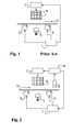
- Figure 1 shows a schematic view of an exemplary film scanner known from the prior art, in which a TDI-CCD image sensor is used.
- a control circuit 1 controls drive motors 2 which transport the film 3 in the direction of the arrow.
- a light source 4 transilluminates the film 3 onto a TDI-CCD image sensor 6.
- Control circuit 1 provides a signal corresponding to the set speed to a control circuit 7, which controls the movement of charges accumulated in one line of a TDI-CCD image sensor 6 to the adjacent line, in accordance with the speed and in the direction of the film transport.
- the set speed must not necessarily correspond with the actual speed, for example due to varying friction in the drive motors and manufacturing tolerances in the take-up and supply reels of the film.
- a method according to the invention is adapted for controlling a scanning apparatus for scanning a continuously moved object.
- the scanning apparatus includes a multiplicity of line scanning devices arranged adjacent to each other in the direction of the movement of the moved object.
- Each of the line scanning devices has a multiplicity of pixels that are arranged adjacent to each other in a direction across a path along which the object is moved.
- the pixels of the line scanning devices accumulate charges according to the amount of incident light.
- a controlling means is provided for transferring the charges accumulated in individual pixels to pixels in the adjacent line scanning device in synchronism with direction of the movement and the speed of the moving object.
- the object is illuminated or transilluminated by a light source. According to the inventive method, the actual momentary position of the moving object is seized, and the time instant or period in which image information is captured by the scanning devices is controlled in dependence of the actual momentary position of the object.
- controlling the time instant or period in which image information is captured by the scanning devices includes transferring the charge of individual pixels representing image information to the adjacent line scanning device in dependence of the actual momentary position of the object.
- a light source which produces light pulses the beginning and duration of which is controlled in dependence of the momentary position of the object.
- only the beginning and duration of the light pulses is controlled in dependence of the momentary position of the object, whereas in another embodiment also the transfer of charges from one CCD line to the next, adjacent CCD line is controlled in dependence of the momentary position of the object.
- beginning and duration of the light pulses is controlled in dependence of the intensity of the light pulses issued by the light source.
- the beginning and duration of the light pulses is controlled in dependence of the amount of light that is required for full exposure of a pixel in the line scanning device. In this way, the dynamic range of the sensor can be fully exploited. In case a section of the film is fully transparent or a part of the object is fully reflective it is also possible to calibrate the light pulses to match the properties of the sensor to the properties of the film or object.
- the film position is detected and the best suited time for moving the charges from one CCD line to the next is determined, thus defining the light integration period, according to the film position. If the film is lit by a pulsed light source the beginning of the integration time is also determined based on the actual film position.
- the film position may be determined by optical or mechanical sensor systems.
- the actual position of the film is taken from the means that are provided for correcting steadiness errors.
- the means that are provided for correcting steadiness errors use marks on the film which have a fixed spatial relationship to the image on the film.
- the pulse duration has to be chosen as short as possible in order to minimise the overlap between adjacent scan areas.
- FIG. 2 shows a schematic block diagram of an exemplary film scanner according to the invention.
- a first control circuit 1 controls the speed of drive motors 2, which transport the film 3 to be scanned in the direction of the arrow.
- a light source 4 transilluminates the film 3 onto a TDI-CCD image sensor arrangement 6.
- Contrary to the prior art means 9 for detecting the film speed and/or position are provided.
- the information about the film speed and/or the film position is supplied to a second control circuit 8.
- the second control circuit 8 supplies the information about the film speed to the first control circuit 1 as a feedback for controlling the speed.
- the information about the film speed and/or the film position is further supplied to a third control circuit 7, which controls exposure and transport from one line to an adjacent line of charges integrated in the TDI-CCD image sensor arrangements 6.
- the means 9 for detecting the film speed and/or position is, for example, a sensor arrangement that scans the sprocket holes on the film.
- the means 9 for detecting the film speed and/or position may also include rollers mechanically engaging with the film and providing information about speed and/or position.
- the means for seizing the actual position of the moving object includes optical or mechanical scanners for scanning features of the object that have a position that is fixed at least with respect to parts of the object.
- Figure 3 shows an embodiment of the inventive film scanner, which essentially corresponds to the embodiment described under figure 2.
- the light source 4 is a pulsed light source. Begin and duration of the light pulses emitted by the light source 4 are controlled by the second control circuit 8, in accordance with information about the speed and/or position of the film 3.
- FIG 4a a number of square areas 'a' to 'I' representing pixels on a film that are located adjacent to each other in the direction of the film transport is shown.
- each pixel would have the same length for a line of CCD image sensors that is arranged across the film.
- the single line of CCD image sensors is represented by the dashed box 10 crossing the square area indexed 'f'.
- the direction of the film transport is indicated by the arrow pointing from left to right.
- the speed of the film transport is not constant, i.e. changes with time.
- the virtual length of each individual square area representing a pixel on the film depends on the momentary transport speed when passing the single line of a CCD image sensor.
- this is indicated by rectangular areas having different lengths.
- the non-constant transport speed results in different periods of time available for integrating light that is falling onto the image sensor for each individual pixel.
- Figures 4a) and 4b) are shown vertically aligned one over each other.
- the same number of pixels or rectangular areas representing the pixels passes along the single line of the CCD image sensor.
- the total length of the pixels passing by in figures 4a) and 4b) is equal.
- the average film transport speed is the same. If the moment in time when the CCD sensor takes an image is calculated based on the average speed the result would be acceptable in case the transport speed is perfectly constant over time. For example, it is desired to acquire an image in the middle of a pixel, as is shown in figure 4a) for the square area indexed 'f'. As the average film transport speed in both, figure 4a) and figure 4b) is equal, the moment in time when the image sensor takes the image is the same.
- the image is not taken in the middle of the pixel indexed 'f' but rather at the transition between the pixels indexed 'f' and 'g'.
- the image sensor even acquires a part of the pixel indexed 'g'. This can result in a drastic reduction of the sharpness of the scanned image.
- TDI-CCD image sensor If a TDI-CCD image sensor is assumed the reduction of the sharpness of the scanned image is even aggravated, in case the charge transfer is not synchronised with the film transport. In this case the charge that is transferred from one line of the image sensor to the next line of the image sensor in a presumed synchronism with the transport speed can be generated from various pixels on the film instead of always being generated by the same pixel on the film.
- the film scanner according to the invention corrects for the variation in the film speed by accordingly controlling begin and end of the integration time and, in case of a TDI-CCD image sensor, the transport of the integrated charge to the adjacent line of image sensor elements such that an image is always taken at a desired position within an area representing a pixel on the film.
- the rectangular sensor area shown in figure 4 is used for clarity only. Although it is conceivable to use sensor areas shaped rectangular as shown in the figure, most image sensors feature square sensor areas having the size of the pixel on the film that is scanned. Due to the non-infinitesimal exposure a minimal amount of smear may be present. This smear occurs when an area belonging to the next following pixel enters the area of the sensor. Even when the charge is transferred in synchronism with the film transport, the charge may contain image information from the desired pixel and the following pixel, as exposure of the sensor continues during the charge transport in the case of constant illumination. However, proper synchronisation of the charge transfer in a TDI-CCD image sensor reduces the overlap of neighbouring pixels. An infinitesimal exposure period, e.g. by a very short light pulse having a very high intensity would further reduce the minimal amount of smear.
- charge integration and charge transfer is synchronised with the actual momentary film transport speed. In this way it is possible to always integrate charges in the CCD elements in a desired position within an area representing a pixel on the film. In the case of a TDI-CCD image sensor the charges are only transferred to the adjacent line of CCD image sensors when the area representing a pixel on the film is actually moving into the scanning range of the adjacent line.
- the light source used for illuminating or transilluminating the film is a pulsed light source.
- the light pulses emitted for illuminating or transilluminating the film may also be triggered in synchronism with the actual momentary transport speed.
- the charges may be transferred to an adjacent line of image sensing elements during the time between two pulses of the light source.
- the pixels or sensor elements of the line scanning device may have at least one effective dimension that is smaller than the corresponding dimension of a respective area on the object that is to be scanned by the respective pixel.
- the width of a sensor element in a direction across the object to be scanned may be given by the length of the sensor line and the desired resolution.
- the dimension of the sensor element of the line sensor in the direction of the film transport may be smaller than the other dimension or the area on the object to be scanned. In that way a rectangular pixel is used in the sensor arrangement rather than a square pixel. This is shown in a diagrammatic way in figure 5.
- the area on the film to be scanned is represented as a square area marked with hashed lines.
- FIG. 5 a) the exposure of the sensor element is triggered in the middle of the area to be scanned.
- the area captured by the sensor element or the active is represented by the white rectangular area. This area may be captured either by a very short, flash-like exposure or by a longer exposure.
- the white area corresponds to the size of the sensor element; in the latter case the sensor element is smaller in the direction of transport of the film.
- Figure 5 b) shows a shift in the time of trigger of exposure. Here, the exposure is triggered later, i.e.
- the image captured on the film is made up from square pixels. Actual cinematographic film, however, does not have a square pixel structure. However, depending on the resolution of the film scanner and the design of the individual photo-sensitive elements of the image sensor, one element of the image sensor acquires an image of an area on the film that is shaped according to the design of the individual elements of the image sensor.
- the foregoing description refers to an exemplary square-shaped element of an image sensor and hence to exemplary square-shaped pixels it is obvious that the principles described above apply to any image sensor that includes individual image sensing elements arranged in a line or in multiple parallel lines.
- CMOS imager pixels which extends over the width of the film and which has a number of pixels arranged in the direction of the transport of the film can be used.
- a full image is taken by the CMOS imager in synchronism with the transport of the film.
- the film has been moved for a distance corresponding to the length of a pixel a new full image is captured. Since the position of the film is known and the time instant when each full image is captured is also known each full image can be unambiguously assigned to pixels on the film. In the same way each pixel of the images taken imager can be unambiguously assigned to an area on the film.
- the respective pixels of images taken subsequently that are belonging to the same area on the film are added afterwards.
- This adding can either take place in the analogue domain, for example in capacitors, or in the digital domain after sampling and analogue-to-digital conversion. Since the respective content of the film does not change over time no reduction in sharpness or blurring due to movement occurs.
- This development of the invention is particularly well-suited to be used together with a pulsed light source.
Landscapes
- Engineering & Computer Science (AREA)
- Multimedia (AREA)
- Signal Processing (AREA)
- Facsimile Scanning Arrangements (AREA)
- Image Input (AREA)
- Transforming Light Signals Into Electric Signals (AREA)
- Facsimile Heads (AREA)
Priority Applications (6)
| Application Number | Priority Date | Filing Date | Title |
|---|---|---|---|
| EP06300593A EP1868366A1 (de) | 2006-06-16 | 2006-06-16 | Verfahren zur Steuerung eines TDI-CCD Bildsensors |
| EP07765330A EP2030432A1 (de) | 2006-06-16 | 2007-06-06 | Verfahren zur steuerung eines tdi-ccd-bildsensors |
| PCT/EP2007/055600 WO2007144304A1 (en) | 2006-06-16 | 2007-06-06 | Method for controlling a tdi-ccd image sensor |
| JP2009514758A JP2009540710A (ja) | 2006-06-16 | 2007-06-06 | Tdi−ccdイメージ・センサを制御する方法 |
| KR1020087028407A KR20090023573A (ko) | 2006-06-16 | 2007-06-06 | Tdi-ccd 이미지 센서를 제어하기 위한 방법 |
| US12/308,497 US8698890B2 (en) | 2006-06-16 | 2007-06-06 | Method for controlling a TDI-CCD image sensor |
Applications Claiming Priority (1)
| Application Number | Priority Date | Filing Date | Title |
|---|---|---|---|
| EP06300593A EP1868366A1 (de) | 2006-06-16 | 2006-06-16 | Verfahren zur Steuerung eines TDI-CCD Bildsensors |
Publications (1)
| Publication Number | Publication Date |
|---|---|
| EP1868366A1 true EP1868366A1 (de) | 2007-12-19 |
Family
ID=38048061
Family Applications (2)
| Application Number | Title | Priority Date | Filing Date |
|---|---|---|---|
| EP06300593A Withdrawn EP1868366A1 (de) | 2006-06-16 | 2006-06-16 | Verfahren zur Steuerung eines TDI-CCD Bildsensors |
| EP07765330A Withdrawn EP2030432A1 (de) | 2006-06-16 | 2007-06-06 | Verfahren zur steuerung eines tdi-ccd-bildsensors |
Family Applications After (1)
| Application Number | Title | Priority Date | Filing Date |
|---|---|---|---|
| EP07765330A Withdrawn EP2030432A1 (de) | 2006-06-16 | 2007-06-06 | Verfahren zur steuerung eines tdi-ccd-bildsensors |
Country Status (5)
| Country | Link |
|---|---|
| US (1) | US8698890B2 (de) |
| EP (2) | EP1868366A1 (de) |
| JP (1) | JP2009540710A (de) |
| KR (1) | KR20090023573A (de) |
| WO (1) | WO2007144304A1 (de) |
Cited By (2)
| Publication number | Priority date | Publication date | Assignee | Title |
|---|---|---|---|---|
| CN101883221A (zh) * | 2010-06-29 | 2010-11-10 | 天津大学 | 在cmos图像传感器中实现tdi的电路及方法 |
| WO2010150494A1 (ja) | 2009-06-25 | 2010-12-29 | Nec東芝スペースシステム株式会社 | 撮像装置、撮像方法及び撮像回路 |
Families Citing this family (6)
| Publication number | Priority date | Publication date | Assignee | Title |
|---|---|---|---|---|
| US20100147951A1 (en) * | 2008-12-11 | 2010-06-17 | Sik Piu Kwan | apparatus, method and system for reducing motion blur in an image capture device |
| KR20150131601A (ko) | 2014-05-15 | 2015-11-25 | 주식회사 뷰웍스 | 양방향 tdi 라인 이미지 센서 |
| KR101653228B1 (ko) | 2014-05-15 | 2016-09-01 | 주식회사 뷰웍스 | Tdi 라인 이미지 센서 |
| CN112087622B (zh) * | 2020-09-15 | 2022-06-17 | 大连海事大学 | 一种tdi-ccd相机反射率分辨率指标模拟测试方法及系统 |
| CN112118441B (zh) * | 2020-09-22 | 2021-06-15 | 中国科学院长春光学精密机械与物理研究所 | 一种位校正改进的串行cmos图像数据训练方法 |
| CN116156342B (zh) * | 2023-04-04 | 2023-06-27 | 合肥埃科光电科技股份有限公司 | 多线阵图像传感器拼接方法、线阵采像系统及装置 |
Citations (8)
| Publication number | Priority date | Publication date | Assignee | Title |
|---|---|---|---|---|
| US4855836A (en) * | 1987-10-15 | 1989-08-08 | Producers Color Service, Inc. | Method and apparatus for converting film to line synchronized video signal data |
| US4896211A (en) * | 1988-04-26 | 1990-01-23 | Picker International, Inc. | Asynchronously triggered single field transfer video camera |
| EP0366235A1 (de) * | 1988-09-26 | 1990-05-02 | Picker International, Inc. | Verfahren und Anordnung zur Überwachung |
| US5040057A (en) * | 1990-08-13 | 1991-08-13 | Picker International, Inc. | Multi-mode TDI/raster-scan television camera system |
| JPH0576005A (ja) * | 1991-09-13 | 1993-03-26 | Nikon Corp | 画像入力装置 |
| EP0543629A1 (de) * | 1991-11-19 | 1993-05-26 | E.I. Du Pont De Nemours And Company | Feststellung von Fehlern |
| US5365084A (en) * | 1991-02-20 | 1994-11-15 | Pressco Technology, Inc. | Video inspection system employing multiple spectrum LED illumination |
| EP0738886A2 (de) * | 1995-04-20 | 1996-10-23 | Eastman Kodak Company | Schichtdichte Analysator und Verfahren zur Verwendung von nicht synchronen TDI Kameras |
Family Cites Families (6)
| Publication number | Priority date | Publication date | Assignee | Title |
|---|---|---|---|---|
| US5562788A (en) * | 1994-09-20 | 1996-10-08 | The Boeing Company | Composite material laser flaw detection |
| US6040057A (en) * | 1997-04-11 | 2000-03-21 | Karen M. Slimak | Enhancing the strength, moisture resistance, and fire-resistance of wood, timber, lumber, similar plant-derived construction and building materials, and other cellulosic materials |
| US6927859B2 (en) * | 2001-03-08 | 2005-08-09 | The Hong Kong Polytechnic University | Microdensitometer system with micrometer resolution for reading radiochromic films |
| US6678395B2 (en) * | 2001-03-22 | 2004-01-13 | Robert N. Yonover | Video search and rescue device |
| IL149587A (en) * | 2001-05-11 | 2005-11-20 | Orbotech Ltd | Optical inspection system employing a staring array scanner |
| US6933975B2 (en) * | 2002-04-26 | 2005-08-23 | Fairchild Imaging | TDI imager with automatic speed optimization |
-
2006
- 2006-06-16 EP EP06300593A patent/EP1868366A1/de not_active Withdrawn
-
2007
- 2007-06-06 EP EP07765330A patent/EP2030432A1/de not_active Withdrawn
- 2007-06-06 WO PCT/EP2007/055600 patent/WO2007144304A1/en not_active Ceased
- 2007-06-06 US US12/308,497 patent/US8698890B2/en not_active Expired - Fee Related
- 2007-06-06 KR KR1020087028407A patent/KR20090023573A/ko not_active Ceased
- 2007-06-06 JP JP2009514758A patent/JP2009540710A/ja not_active Withdrawn
Patent Citations (9)
| Publication number | Priority date | Publication date | Assignee | Title |
|---|---|---|---|---|
| US4855836A (en) * | 1987-10-15 | 1989-08-08 | Producers Color Service, Inc. | Method and apparatus for converting film to line synchronized video signal data |
| US4896211A (en) * | 1988-04-26 | 1990-01-23 | Picker International, Inc. | Asynchronously triggered single field transfer video camera |
| EP0366235A1 (de) * | 1988-09-26 | 1990-05-02 | Picker International, Inc. | Verfahren und Anordnung zur Überwachung |
| EP0366235B2 (de) * | 1988-09-26 | 2004-01-07 | Picker International, Inc. | Verfahren und Anordnung zur Überwachung |
| US5040057A (en) * | 1990-08-13 | 1991-08-13 | Picker International, Inc. | Multi-mode TDI/raster-scan television camera system |
| US5365084A (en) * | 1991-02-20 | 1994-11-15 | Pressco Technology, Inc. | Video inspection system employing multiple spectrum LED illumination |
| JPH0576005A (ja) * | 1991-09-13 | 1993-03-26 | Nikon Corp | 画像入力装置 |
| EP0543629A1 (de) * | 1991-11-19 | 1993-05-26 | E.I. Du Pont De Nemours And Company | Feststellung von Fehlern |
| EP0738886A2 (de) * | 1995-04-20 | 1996-10-23 | Eastman Kodak Company | Schichtdichte Analysator und Verfahren zur Verwendung von nicht synchronen TDI Kameras |
Cited By (4)
| Publication number | Priority date | Publication date | Assignee | Title |
|---|---|---|---|---|
| WO2010150494A1 (ja) | 2009-06-25 | 2010-12-29 | Nec東芝スペースシステム株式会社 | 撮像装置、撮像方法及び撮像回路 |
| EP2448252A4 (de) * | 2009-06-25 | 2012-11-28 | Nec Toshiba Space Sys Ltd | Bildaufnahmevorrichtung, bildaufnahmeverfahren und bildaufnahmeschaltung |
| US9357100B2 (en) | 2009-06-25 | 2016-05-31 | Nec Corporation | Image capturing apparatus, image capturing method, and image capturing circuit |
| CN101883221A (zh) * | 2010-06-29 | 2010-11-10 | 天津大学 | 在cmos图像传感器中实现tdi的电路及方法 |
Also Published As
| Publication number | Publication date |
|---|---|
| US8698890B2 (en) | 2014-04-15 |
| US20100238522A1 (en) | 2010-09-23 |
| WO2007144304A1 (en) | 2007-12-21 |
| EP2030432A1 (de) | 2009-03-04 |
| KR20090023573A (ko) | 2009-03-05 |
| JP2009540710A (ja) | 2009-11-19 |
Similar Documents
| Publication | Publication Date | Title |
|---|---|---|
| US8698890B2 (en) | Method for controlling a TDI-CCD image sensor | |
| JP3091969B2 (ja) | ビデオカメラ | |
| US9426400B2 (en) | Method and apparatus for high speed acquisition of moving images using pulsed illumination | |
| EP0665694B1 (de) | Hochauflösender Filmabtaster | |
| JPH08292159A (ja) | 非同期tdiカメラを使用した被覆密度分析器及び分析方法 | |
| US5750985A (en) | High speed and high precisioin image scanning apparatus | |
| US6933975B2 (en) | TDI imager with automatic speed optimization | |
| US4278999A (en) | Moving image scanner | |
| KR100939390B1 (ko) | 화상 판독 장치 및 방법 | |
| US8004724B2 (en) | Method and apparatus for image reading with synchronized readout and lighting control | |
| US6201619B1 (en) | Autofocus process and system with fast multi-region sampling | |
| US6683293B1 (en) | TDI imager with target synchronization | |
| JP6838348B2 (ja) | 画像読取装置および画像読取方法 | |
| US7345796B2 (en) | Image scanner for use in image forming apparatus | |
| CN1135829C (zh) | 图象扫描装置 | |
| US20020131060A1 (en) | Process and apparatus for the digital production of a picture | |
| JP2004188845A (ja) | プリントヘッドの特性計測装置、露光量補正方法、および画像形成装置 | |
| US20050105144A1 (en) | Image reading apparatus | |
| US6906833B1 (en) | Constant speed image reading device and method | |
| JP2000201250A (ja) | 走行物体撮像方法及びラインスキャナ装置 | |
| JP4967109B2 (ja) | 撮像装置 | |
| JP4426131B2 (ja) | 走査光学系の走査ビーム測定評価方法及び測定評価装置 | |
| EP1009159A2 (de) | Abtastvorrichtung mit mehreren Photosensorreihen | |
| KR100268340B1 (ko) | 셔틀방식 스캐너의 쉐이딩 보정방법 | |
| JPH1098649A (ja) | Ccdラインセンサ |
Legal Events
| Date | Code | Title | Description |
|---|---|---|---|
| PUAI | Public reference made under article 153(3) epc to a published international application that has entered the european phase |
Free format text: ORIGINAL CODE: 0009012 |
|
| AK | Designated contracting states |
Kind code of ref document: A1 Designated state(s): AT BE BG CH CY CZ DE DK EE ES FI FR GB GR HU IE IS IT LI LT LU LV MC NL PL PT RO SE SI SK TR |
|
| AX | Request for extension of the european patent |
Extension state: AL BA HR MK YU |
|
| AKX | Designation fees paid | ||
| STAA | Information on the status of an ep patent application or granted ep patent |
Free format text: STATUS: THE APPLICATION IS DEEMED TO BE WITHDRAWN |
|
| 18D | Application deemed to be withdrawn |
Effective date: 20080620 |
|
| REG | Reference to a national code |
Ref country code: DE Ref legal event code: 8566 |