EP1882985A2 - Appareil lithographique et procédé de fabrication du dispositif - Google Patents
Appareil lithographique et procédé de fabrication du dispositif Download PDFInfo
- Publication number
- EP1882985A2 EP1882985A2 EP07075633A EP07075633A EP1882985A2 EP 1882985 A2 EP1882985 A2 EP 1882985A2 EP 07075633 A EP07075633 A EP 07075633A EP 07075633 A EP07075633 A EP 07075633A EP 1882985 A2 EP1882985 A2 EP 1882985A2
- Authority
- EP
- European Patent Office
- Prior art keywords
- correction signal
- stage
- disturbance torque
- supports
- substrate
- Prior art date
- Legal status (The legal status is an assumption and is not a legal conclusion. Google has not performed a legal analysis and makes no representation as to the accuracy of the status listed.)
- Granted
Links
Images


Classifications
-
- H—ELECTRICITY
- H10—SEMICONDUCTOR DEVICES; ELECTRIC SOLID-STATE DEVICES NOT OTHERWISE PROVIDED FOR
- H10P—GENERIC PROCESSES OR APPARATUS FOR THE MANUFACTURE OR TREATMENT OF DEVICES COVERED BY CLASS H10
- H10P76/00—Manufacture or treatment of masks on semiconductor bodies, e.g. by lithography or photolithography
- H10P76/20—Manufacture or treatment of masks on semiconductor bodies, e.g. by lithography or photolithography of masks comprising organic materials
- H10P76/204—Manufacture or treatment of masks on semiconductor bodies, e.g. by lithography or photolithography of masks comprising organic materials of organic photoresist masks
- H10P76/2041—Photolithographic processes
-
- G—PHYSICS
- G03—PHOTOGRAPHY; CINEMATOGRAPHY; ANALOGOUS TECHNIQUES USING WAVES OTHER THAN OPTICAL WAVES; ELECTROGRAPHY; HOLOGRAPHY
- G03F—PHOTOMECHANICAL PRODUCTION OF TEXTURED OR PATTERNED SURFACES, e.g. FOR PRINTING, FOR PROCESSING OF SEMICONDUCTOR DEVICES; MATERIALS THEREFOR; ORIGINALS THEREFOR; APPARATUS SPECIALLY ADAPTED THEREFOR
- G03F7/00—Photomechanical, e.g. photolithographic, production of textured or patterned surfaces, e.g. printing surfaces; Materials therefor, e.g. comprising photoresists; Apparatus specially adapted therefor
- G03F7/70—Microphotolithographic exposure; Apparatus therefor
- G03F7/70691—Handling of masks or workpieces
- G03F7/70716—Stages
- G03F7/70725—Stages control
Definitions
- the invention relates to a control system to control a position parameter of a stage in a lithographic apparatus, to a lithographic apparatus including such control system and to a device manufacturing method.
- controllers may be present operating in X, Y, Z, Rx, Ry, Rz coordinates, the latter three describing rotations around the X, Y and Z axes, respectively.
- each of these controllers generates a controller force or torque (i.e. a controller output signal to drive an actuator which actuator will thereby generate a force or torque) as a response to the deviation of the actually measured position in its coordinate system fom the corresponding position set-point.
- the forces and torques calculated this way by the controllers are also defined in the coordinate system as defined above, related to the lens center.
- the gain scheduling matrix then generates an extra force in Z that makes sure the substrate remains in the focal plane of the lens, and hence the table actually tilts around the X axis as defined by the coordinate system described above related to the lens, instead of tilting around a line extending in X direction, crossing the center of mass of the stage.
- the generated extra force in Z is proportional to the controller-generated torque around the X axis, the distance of the stage center of mass with respect to the coordinate system origin in Y direction and the stage mass, and inversely proportional to the inertia of the stage around the X axis.
- disturbance forces and disturbance torques act directly on the stage, as they naturally do not follow the gain scheduling compensation used for controller-generated forces and torques.
- disturbance torques do have an influence on other directions.
- a disturbance torque which would tend to tilt the stage with respect to an axis extending along the plane of focus of the projection system and through the center of mass of the stage, would result in a vertical position error of the target portion under the lens center because of the tilting of the stage.
- the term vertical should be understood as being a direction perpendicular to the plane of focus.
- disturbance torques may result in focus errors hence resulting in a deterioration of an accuracy of the pattern to be projected on to the substrate.
- a control system to control a position parameter of a stage in a lithographic apparatus, the control system including, a stage controller to control a position parameter of the stage in at least a first direction, a disturbance torque estimator to estimate a disturbance torque on the stage, the disturbance torque about an axis extending in a second direction, the second direction being substantially perpendicular to the first direction, a correction signal calculator, the correction signal calculator being provided with the estimated disturbance torque and with a signal representative of a position of the stage in a third direction, the third direction being substantially perpendicular to the first and second directions, the correction signal calculator to determine a feedforward correction signal to correct a position error of the stage in the first direction due to the disturbance torque, the feedforward correction signal to be fed to the stage.
- a lithographic apparatus to transfer a pattern on to a substrate, the lithographic apparatus including a stage to hold the substrate and a control system according to the above embodiment of the invention, to control a position of the stage.
- a device manufacturing method including irradiating a pattern on to a substrate by a lithographic apparatus according to an embodiment of the invention; developing the irradiated substrate; and manufacturing a device from the developed substrate.
- a lithographic apparatus including an illumination system configured to condition a beam of radiation; a patterning device support configured to support a patterning device, the patterning device configured to pattern the beam of radiation to form a patterned beam of radiation; a substrate support configured to support a substrate; a projection system configured to project the patterned beam of radiation onto the substrate, and a control system configured to control a position parameter of one of the supports, the control system including a stage controller configured to control a position parameter of the one of the supports in at least a first direction; a disturbance torque estimator configured to estimate a disturbance torque on the one of the supports about an axis extending in a second direction, the second direction being substantially perpendicular to the first direction; and a correction signal calculator, the correction signal calculator adapted to receive the estimated disturbance torque and a signal representative of a position of the one of the supports in a third direction, the third direction being substantially perpendicular to the first and second directions, the correction signal calculator configured to determine a feedforward correction signal
- a device manufacturing method including conditioning a beam of radiation; patterning the beam of radiation to form a patterned beam of radiation with a patterning device, the patterning device supported by a patterning device support; projecting the patterned beam of radiation onto a substrate, the substrate supported by a substrate support; and controlling a position parameter of one of the supports with a control system, the control system including a stage controller configured to control a position parameter of the one of the supports in at least a first direction; a disturbance torque estimator configured to estimate a disturbance torque on the one of the supports about an axis extending in a second direction, the second direction being substantially perpendicular to the first direction; and a correction signal calculator, the correction signal calculator adapted to receive the estimated disturbance torque and a signal representative of a position of the one of the supports in a third direction, the third direction being substantially perpendicular to the first and second directions, the correction signal calculator configured to determine a feedforward correction signal to correct a position error of the one of the supports in
- Figure 1 depicts a lithographic apparatus according to an embodiment of the invention
- Figure 2 depicts a control diagram of a controller according to an embodiment of the invention
- Figure 3 depicts an example of the gain scheduling matrix of Figure 2
- Figure 4 and 4b depict a time diagram of a response of a conventional control system in comparison with a control system according to an embodiment of the invention.
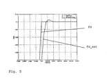
- Figure 5 depicts a time diagram of the disturbance torque amodeled and an estimation of the disturbance.
- FIG. 1 schematically depicts a lithographic apparatus according to one embodiment of the invention.
- the apparatus includes an illumination system (illuminator) IL configured to condition a radiation beam B (e.g. UV radiation or any other suitable radiation), a mask support structure (e.g. a mask table) MT constructed to support a patterning device (e.g. a mask) MA and connected to a first positioning device PM configured to accurately position the patterning device in accordance with certain parameters.
- the apparatus also includes a substrate table (e.g. a wafer table) WT or "substrate support" constructed to hold a substrate (e.g. a resist-coated wafer) W and connected to a second positioning device PW configured to accurately position the substrate in accordance with certain parameters.
- a radiation beam B e.g. UV radiation or any other suitable radiation
- a mask support structure e.g. a mask table
- MT constructed to support a patterning device (e.g. a mask) MA and connected to a
- the apparatus further includes a projection system (e.g. a refractive projection lens system) PS configured to project a pattern imparted to the radiation beam B by patterning device MA onto a target portion C (e.g. including one or more dies) of the substrate W.
- a projection system e.g. a refractive projection lens system
- PS configured to project a pattern imparted to the radiation beam B by patterning device MA onto a target portion C (e.g. including one or more dies) of the substrate W.
- the illumination system may include various types of optical components, such as refractive, reflective, magnetic, electromagnetic, electrostatic or other types of optical components, or any combination thereof, for directing, shaping, or controlling radiation.
- optical components such as refractive, reflective, magnetic, electromagnetic, electrostatic or other types of optical components, or any combination thereof, for directing, shaping, or controlling radiation.
- patterning device used herein should be broadly interpreted as referring to any device that can be used to impart a radiation beam with a pattern in its cross-section so as to create a pattern in a target portion of the substrate. It should be noted that the pattern imparted to the radiation beam may not exactly correspond to the desired pattern in the target portion of the substrate, for example if the pattern includes phase-shifting features or so called assist features. Generally, the pattern imparted to the radiation beam will correspond to a particular functional layer in a device being created in the target portion, such as an integrated circuit.
- projection system used herein should be broadly interpreted as encompassing any type of projection system, including refractive, reflective, catadioptric, magnetic, electromagnetic and electrostatic optical systems, or any combination thereof, as appropriate for the exposure radiation being used, or for other factors such as the use of an immersion liquid or the use of a vacuum. Any use of the term “projection lens” herein may be considered as synonymous with the more general term “projection system”.
- the apparatus is of a transmissive type (e.g. employing a transmissive mask).
- the apparatus may be of a reflective type (e.g. employing a programmable mirror array of a type as referred to above, or employing a reflective mask).
- the lithographic apparatus may be of a type having two (dual stage) or more substrate tables or “substrate supports” (and/or two or more mask tables or “mask supports”).
- substrate tables or “substrate supports” and/or two or more mask tables or “mask supports”
- additional tables or supports may be used in parallel, or preparatory steps may be carried out on one or more tables or supports while one or more other tables or supports are being used for exposure.
- the lithographic apparatus may also be of a type wherein at least a portion of the substrate may be covered by a liquid having a relatively high refractive index, e.g. water, so as to fill a space between the projection system and the substrate.
- a liquid having a relatively high refractive index e.g. water
- An immersion liquid may also be applied to other spaces in the lithographic apparatus, for example, between the mask and the projection system. Immersion techniques can be used to increase the numerical aperture of projection systems.
- immersion as used herein does not mean that a structure, such as a substrate, must be submerged in liquid, but rather only means that a liquid is located between the projection system and the substrate during exposure.
- the illuminator IL may include an adjuster AD configured to adjust the angular intensity distribution of the radiation beam. Generally, at least the outer and/or inner radial extent (commonly referred to as ⁇ -outer and ⁇ -inner, respectively) of the intensity distribution in a pupil plane of the illuminator can be adjusted.
- the illuminator IL may include various other components, such as an integrator IN and a condenser CO. The illuminator may be used to condition the radiation beam, to have a desired uniformity and intensity distribution in its cross-section.
- the depicted apparatus could be used in at least one of the following modes:
- Each of the control loops is provided with a set point Rx, Ry, Z, indicated at a left side of Figure 2, a controller (Rx contr, Ry contr and Z contr) and a feedback path from an output of process P which in this example represents the stage and its actuators, to a subtraction point where the feedback signal is subtracted from the set point signal, an output thereof being provided to the respective controller.
- Figure 2 depicts a gain-scheduling matrix GS which provides for an X, Y position dependent compensation of controller outputs (e.g. controller signals which represent a force).
- the gain scheduling matrix which is included in the exemplary embodiment in the Rx, Ry and Z feedback loop, could be omitted. In that case, controller-generated torques are not fed through the gain scheduling matrix to avoid position errors, as described above.
- a disturbance torque estimator is provided to estimate a disturbance torque Fd_est, as indicated in Figure 2.
- the estimated disturbance torque is in this example about an axis extending in X direction, thus an Rx disturbance torque.
- Such disturbance torque would result in a tilting of the stage about its center of mass, which would result in a position dependent focus error of the stage, as the tilting about the axis extending in the X direction will result in a Z displacement of the target portion if the center of mass of the substrate table is not positioned under the lens center.
- the matrix depicted in Figure 3 may not only be used as the correction signal calculator GS', however may also be applied as the gain-scheduling matrix GS.
- the correction signal calculator thereby includes a copy of the gain-scheduling matrix GS.
- the F x , F y and F z inputs as well as the T Rx , T Ry , T Rz outputs of the correction signal calculator GS' may not be connected.
- one of the two branches may be omitted, also depending on the frequency range of the disturbance torques.
- Figures 4a and 4b show a time diagram of a disturbance torque which shows a stepwise function, a response in Z direction thereto without the compensation as described above, indicated by Z 1 ) and a response including the correction described above (indicated by Z 2 ).
- an error of two microradians about an axis extending in X direction results.
- an error in Z direction thus in a direction substantially perpendicular to the focal plane, results, indicated by Z1 in Figure 4b.
- this error is reduced by the feedback loop.
- the substrate referred to herein may be processed, before or after exposure, in for example a track (a tool that typically applies a layer of resist to a substrate and develops the exposed resist), a metrology tool and/or an inspection tool. Where applicable, the disclosure herein may be applied to such and other substrate processing tools. Further, the substrate may be processed more than once, for example in order to create a multi-layer IC, so that the term substrate used herein may also refer to a substrate that already contains multiple processed layers.
Landscapes
- Physics & Mathematics (AREA)
- General Physics & Mathematics (AREA)
- Exposure And Positioning Against Photoresist Photosensitive Materials (AREA)
- Exposure Of Semiconductors, Excluding Electron Or Ion Beam Exposure (AREA)
- Control Of Position Or Direction (AREA)
- Feedback Control In General (AREA)
Applications Claiming Priority (1)
| Application Number | Priority Date | Filing Date | Title |
|---|---|---|---|
| US11/491,493 US7630059B2 (en) | 2006-07-24 | 2006-07-24 | Lithographic apparatus and device manufacturing method |
Publications (3)
| Publication Number | Publication Date |
|---|---|
| EP1882985A2 true EP1882985A2 (fr) | 2008-01-30 |
| EP1882985A3 EP1882985A3 (fr) | 2009-07-29 |
| EP1882985B1 EP1882985B1 (fr) | 2010-12-15 |
Family
ID=38441869
Family Applications (1)
| Application Number | Title | Priority Date | Filing Date |
|---|---|---|---|
| EP07075633A Active EP1882985B1 (fr) | 2006-07-24 | 2007-07-24 | Appareil lithographique et procédé de fabrication du dispositif |
Country Status (8)
| Country | Link |
|---|---|
| US (1) | US7630059B2 (fr) |
| EP (1) | EP1882985B1 (fr) |
| JP (1) | JP4734298B2 (fr) |
| KR (1) | KR100869308B1 (fr) |
| CN (1) | CN100565351C (fr) |
| DE (1) | DE602007011160D1 (fr) |
| SG (1) | SG139663A1 (fr) |
| TW (1) | TWI356276B (fr) |
Families Citing this family (16)
| Publication number | Priority date | Publication date | Assignee | Title |
|---|---|---|---|---|
| NL1036662A1 (nl) * | 2008-04-08 | 2009-10-09 | Asml Netherlands Bv | Stage system and lithographic apparatus comprising such stage system. |
| NL2003993A (nl) * | 2009-01-22 | 2010-07-26 | Asml Netherlands Bv | Control system, lithographic apparatus and a method to control a position quantity of a control location of a movable object. |
| JP5235707B2 (ja) * | 2009-02-03 | 2013-07-10 | キヤノン株式会社 | 制御装置 |
| JP5349093B2 (ja) * | 2009-03-16 | 2013-11-20 | 株式会社日立ハイテクノロジーズ | プロキシミティ露光装置、プロキシミティ露光装置の基板位置決め方法、及び表示用パネル基板の製造方法 |
| NL2005013A (en) * | 2009-07-31 | 2011-02-02 | Asml Netherlands Bv | Positioning system, lithographic apparatus and method. |
| NL2006804A (en) * | 2010-06-24 | 2011-12-28 | Asml Netherlands Bv | Measurement system, method and lithographic apparatus. |
| NL2006981A (en) * | 2010-07-26 | 2012-01-30 | Asml Netherlands Bv | Position control system, lithographic apparatus, and method to control a position of a movable object. |
| NL2007606A (en) * | 2010-11-22 | 2012-05-23 | Asml Netherlands Bv | Controller, lithographic apparatus, method of controlling the position of an object and device manufacturing method. |
| CN102087482B (zh) * | 2010-12-27 | 2012-10-03 | 中国科学院光电技术研究所 | 光刻机工件台同步运动误差校正控制系统 |
| CN102768468B (zh) | 2011-05-03 | 2015-07-22 | 上海微电子装备有限公司 | 用于光刻设备的粗动台的质心测校的方法 |
| NL2010456A (en) * | 2012-04-18 | 2013-10-21 | Asml Holding Nv | Lithographic apparatuses and methods for compensating for eigenmode coupling. |
| EP4094799A1 (fr) * | 2013-03-12 | 2022-11-30 | Corium, Inc. | Applicateurs de microprojection |
| US10120293B2 (en) * | 2013-10-30 | 2018-11-06 | Asml Netherlands B.V. | Object positioning in lithography |
| NL2014562A (en) * | 2014-04-04 | 2015-10-13 | Asml Netherlands Bv | Control system, positioning system, lithographic apparatus, control method, device manufacturing method and control program. |
| WO2015191809A1 (fr) | 2014-06-11 | 2015-12-17 | Dignity Health | Systèmes et procédés de détection de mensonge non-intrusive |
| JP7148295B2 (ja) | 2018-07-04 | 2022-10-05 | キヤノン株式会社 | 制御装置、露光装置及び物品の製造方法 |
Family Cites Families (20)
| Publication number | Priority date | Publication date | Assignee | Title |
|---|---|---|---|---|
| JP3215280B2 (ja) * | 1995-03-02 | 2001-10-02 | キヤノン株式会社 | ステージ位置決め制御装置 |
| JP3733174B2 (ja) * | 1996-06-19 | 2006-01-11 | キヤノン株式会社 | 走査型投影露光装置 |
| JPH11150062A (ja) * | 1997-11-14 | 1999-06-02 | Nikon Corp | 除振装置及び露光装置並びに除振台の除振方法 |
| US6287735B2 (en) | 1998-09-16 | 2001-09-11 | Nikon Corporation | Method and apparatus for controlling the leveling table of a wafer stage |
| EP1164352A4 (fr) * | 1999-02-17 | 2007-09-05 | Nikon Corp | Procede de detection de position et detecteur de position, procede d'exposition et appareil correspondant, dispositif et procede de fabrication de ce dispositif |
| JP3298069B2 (ja) * | 1999-05-20 | 2002-07-02 | 住友重機械工業株式会社 | ステージの位置制御装置及び速度制御装置 |
| JP3312297B2 (ja) * | 1999-07-02 | 2002-08-05 | 住友重機械工業株式会社 | ステージ位置制御装置 |
| US6504162B1 (en) * | 2000-09-15 | 2003-01-07 | Nikon Corporation | Stage device, control system, and method for stabilizing wafer stage and wafer table |
| JP3932039B2 (ja) * | 2000-10-19 | 2007-06-20 | 株式会社ニコン | 位置検出方法、位置検出装置、露光方法、露光装置、制御プログラム、及びデバイス製造方法 |
| AU2002306892A1 (en) * | 2001-03-26 | 2002-10-08 | Cymer, Inc. | Method and device for vibration control |
| JP2003264133A (ja) * | 2002-03-08 | 2003-09-19 | Nikon Corp | ステージ制御装置、露光装置、デバイス製造方法、及びステージ制御方法 |
| JP2003264134A (ja) * | 2002-03-08 | 2003-09-19 | Nikon Corp | ステージ制御装置、露光装置、及びデバイス製造方法 |
| JP2004100953A (ja) * | 2002-08-23 | 2004-04-02 | Nikon Corp | 制振装置及び露光装置 |
| JP2005051197A (ja) * | 2003-07-17 | 2005-02-24 | Nikon Corp | ステージ制御方法及び装置、ステージ制御プログラム、露光装置、並びにデバイス製造方法 |
| TWI254190B (en) * | 2003-09-22 | 2006-05-01 | Asml Netherlands Bv | Lithographic apparatus, device manufacturing method, and device manufactured thereby |
| US7289858B2 (en) * | 2004-05-25 | 2007-10-30 | Asml Netherlands B.V. | Lithographic motion control system and method |
| JP4493484B2 (ja) * | 2004-11-29 | 2010-06-30 | 株式会社日立ハイテクノロジーズ | アクティブ除振方法及び装置 |
| US7327437B2 (en) | 2004-12-07 | 2008-02-05 | Asml Netherlands B.V. | Lithographic apparatus and device manufacturing method |
| US7307262B2 (en) * | 2004-12-23 | 2007-12-11 | Asml Netherlands B.V. | Lithographic apparatus and device manufacturing method |
| US7265813B2 (en) * | 2004-12-28 | 2007-09-04 | Asml Netherlands B.V. | Lithographic apparatus and device manufacturing method |
-
2006
- 2006-07-24 US US11/491,493 patent/US7630059B2/en active Active
-
2007
- 2007-07-12 SG SG200705201-2A patent/SG139663A1/en unknown
- 2007-07-17 TW TW096126045A patent/TWI356276B/zh active
- 2007-07-17 JP JP2007185824A patent/JP4734298B2/ja active Active
- 2007-07-23 KR KR1020070073361A patent/KR100869308B1/ko active Active
- 2007-07-24 DE DE602007011160T patent/DE602007011160D1/de active Active
- 2007-07-24 CN CNB2007101386396A patent/CN100565351C/zh active Active
- 2007-07-24 EP EP07075633A patent/EP1882985B1/fr active Active
Non-Patent Citations (1)
| Title |
|---|
| None |
Also Published As
| Publication number | Publication date |
|---|---|
| CN101114133A (zh) | 2008-01-30 |
| DE602007011160D1 (de) | 2011-01-27 |
| CN100565351C (zh) | 2009-12-02 |
| US7630059B2 (en) | 2009-12-08 |
| KR20080009649A (ko) | 2008-01-29 |
| TWI356276B (en) | 2012-01-11 |
| EP1882985A3 (fr) | 2009-07-29 |
| KR100869308B1 (ko) | 2008-11-18 |
| EP1882985B1 (fr) | 2010-12-15 |
| JP4734298B2 (ja) | 2011-07-27 |
| SG139663A1 (en) | 2008-02-29 |
| US20080018877A1 (en) | 2008-01-24 |
| TW200821736A (en) | 2008-05-16 |
| JP2008028392A (ja) | 2008-02-07 |
Similar Documents
| Publication | Publication Date | Title |
|---|---|---|
| EP1882985B1 (fr) | Appareil lithographique et procédé de fabrication du dispositif | |
| EP2261739B1 (fr) | Procédé et dispositif pour la création de structures superposées sur un substrat | |
| US8300208B2 (en) | Lithographic apparatus and a method to compensate for the effect of disturbances on the projection system of a lithographic apparatus | |
| EP1843210A2 (fr) | Méthode d'alignement et d'exposition d'un substrat | |
| US7948609B2 (en) | Lithographic apparatus, stage system and stage control method | |
| US20090046260A1 (en) | Lithographic apparatus and thermal optical manipulator control method | |
| US7525638B2 (en) | Lithographic apparatus and device manufacturing method | |
| CN101566854A (zh) | 位置控制系统、光刻设备及控制可移动物体的位置的方法 | |
| US20190179233A1 (en) | A positioning system, method to position, lithographic apparatus and device manufacturing method | |
| US7468782B2 (en) | Lithographic apparatus, position quantity controller and control method with feedforward signal | |
| US7256866B2 (en) | Lithographic apparatus and device manufacturing method | |
| CN102298269B (zh) | 测量系统、方法和光刻设备 | |
| EP3084525B1 (fr) | Appareil lithographique et méthode de fabrication d'un dispositif | |
| US11454938B2 (en) | Control system, method to increase a bandwidth of a control system, and lithographic apparatus | |
| US7352436B2 (en) | Lithographic apparatus, projection apparatus and device manufacturing method | |
| EP1801657A1 (fr) | Procédé de fabrication d'un dispositif et programme d'ordinateur | |
| US7148954B2 (en) | Lithographic apparatus and method for its use | |
| NL2020279A (en) | Lithographic Apparatus Imaging Error Correction |
Legal Events
| Date | Code | Title | Description |
|---|---|---|---|
| PUAI | Public reference made under article 153(3) epc to a published international application that has entered the european phase |
Free format text: ORIGINAL CODE: 0009012 |
|
| AK | Designated contracting states |
Kind code of ref document: A2 Designated state(s): AT BE BG CH CY CZ DE DK EE ES FI FR GB GR HU IE IS IT LI LT LU LV MC MT NL PL PT RO SE SI SK TR |
|
| AX | Request for extension of the european patent |
Extension state: AL BA HR MK YU |
|
| PUAL | Search report despatched |
Free format text: ORIGINAL CODE: 0009013 |
|
| AK | Designated contracting states |
Kind code of ref document: A3 Designated state(s): AT BE BG CH CY CZ DE DK EE ES FI FR GB GR HU IE IS IT LI LT LU LV MC MT NL PL PT RO SE SI SK TR |
|
| AX | Request for extension of the european patent |
Extension state: AL BA HR MK RS |
|
| 17P | Request for examination filed |
Effective date: 20091102 |
|
| 17Q | First examination report despatched |
Effective date: 20100126 |
|
| AKX | Designation fees paid |
Designated state(s): DE FR |
|
| GRAP | Despatch of communication of intention to grant a patent |
Free format text: ORIGINAL CODE: EPIDOSNIGR1 |
|
| GRAS | Grant fee paid |
Free format text: ORIGINAL CODE: EPIDOSNIGR3 |
|
| GRAA | (expected) grant |
Free format text: ORIGINAL CODE: 0009210 |
|
| AK | Designated contracting states |
Kind code of ref document: B1 Designated state(s): DE FR |
|
| REF | Corresponds to: |
Ref document number: 602007011160 Country of ref document: DE Date of ref document: 20110127 Kind code of ref document: P |
|
| PLBE | No opposition filed within time limit |
Free format text: ORIGINAL CODE: 0009261 |
|
| STAA | Information on the status of an ep patent application or granted ep patent |
Free format text: STATUS: NO OPPOSITION FILED WITHIN TIME LIMIT |
|
| 26N | No opposition filed |
Effective date: 20110916 |
|
| REG | Reference to a national code |
Ref country code: DE Ref legal event code: R097 Ref document number: 602007011160 Country of ref document: DE Effective date: 20110916 |
|
| REG | Reference to a national code |
Ref country code: FR Ref legal event code: PLFP Year of fee payment: 10 |
|
| REG | Reference to a national code |
Ref country code: FR Ref legal event code: PLFP Year of fee payment: 11 |
|
| REG | Reference to a national code |
Ref country code: FR Ref legal event code: PLFP Year of fee payment: 12 |
|
| P01 | Opt-out of the competence of the unified patent court (upc) registered |
Effective date: 20230403 |
|
| PGFP | Annual fee paid to national office [announced via postgrant information from national office to epo] |
Ref country code: DE Payment date: 20250728 Year of fee payment: 19 |
|
| PGFP | Annual fee paid to national office [announced via postgrant information from national office to epo] |
Ref country code: FR Payment date: 20250725 Year of fee payment: 19 |