EP1883111A2 - Dispositif de capture d'images et son procédé de fabrication - Google Patents
Dispositif de capture d'images et son procédé de fabrication Download PDFInfo
- Publication number
- EP1883111A2 EP1883111A2 EP07019811A EP07019811A EP1883111A2 EP 1883111 A2 EP1883111 A2 EP 1883111A2 EP 07019811 A EP07019811 A EP 07019811A EP 07019811 A EP07019811 A EP 07019811A EP 1883111 A2 EP1883111 A2 EP 1883111A2
- Authority
- EP
- European Patent Office
- Prior art keywords
- semiconductor substrate
- reading part
- fop
- package
- ccd reading
- Prior art date
- Legal status (The legal status is an assumption and is not a legal conclusion. Google has not performed a legal analysis and makes no representation as to the accuracy of the status listed.)
- Granted
Links
Images





Classifications
-
- H—ELECTRICITY
- H01—ELECTRIC ELEMENTS
- H01J—ELECTRIC DISCHARGE TUBES OR DISCHARGE LAMPS
- H01J37/00—Discharge tubes with provision for introducing objects or material to be exposed to the discharge, e.g. for the purpose of examination or processing thereof
- H01J37/02—Details
- H01J37/22—Optical, image processing or photographic arrangements associated with the tube
- H01J37/224—Luminescent screens or photographic plates for imaging; Apparatus specially adapted therefor, e. g. cameras, TV-cameras, photographic equipment or exposure control; Optical subsystems specially adapted therefor, e. g. microscopes for observing image on luminescent screen
-
- H—ELECTRICITY
- H01—ELECTRIC ELEMENTS
- H01J—ELECTRIC DISCHARGE TUBES OR DISCHARGE LAMPS
- H01J37/00—Discharge tubes with provision for introducing objects or material to be exposed to the discharge, e.g. for the purpose of examination or processing thereof
- H01J37/02—Details
- H01J37/244—Detectors; Associated components or circuits therefor
-
- H—ELECTRICITY
- H04—ELECTRIC COMMUNICATION TECHNIQUE
- H04N—PICTORIAL COMMUNICATION, e.g. TELEVISION
- H04N23/00—Cameras or camera modules comprising electronic image sensors; Control thereof
- H04N23/50—Constructional details
- H04N23/54—Mounting of pick-up tubes, electronic image sensors, deviation or focusing coils
-
- H—ELECTRICITY
- H04—ELECTRIC COMMUNICATION TECHNIQUE
- H04N—PICTORIAL COMMUNICATION, e.g. TELEVISION
- H04N23/00—Cameras or camera modules comprising electronic image sensors; Control thereof
- H04N23/50—Constructional details
- H04N23/55—Optical parts specially adapted for electronic image sensors; Mounting thereof
-
- H—ELECTRICITY
- H10—SEMICONDUCTOR DEVICES; ELECTRIC SOLID-STATE DEVICES NOT OTHERWISE PROVIDED FOR
- H10F—INORGANIC SEMICONDUCTOR DEVICES SENSITIVE TO INFRARED RADIATION, LIGHT, ELECTROMAGNETIC RADIATION OF SHORTER WAVELENGTH OR CORPUSCULAR RADIATION
- H10F39/00—Integrated devices, or assemblies of multiple devices, comprising at least one element covered by group H10F30/00, e.g. radiation detectors comprising photodiode arrays
- H10F39/80—Constructional details of image sensors
-
- H—ELECTRICITY
- H10—SEMICONDUCTOR DEVICES; ELECTRIC SOLID-STATE DEVICES NOT OTHERWISE PROVIDED FOR
- H10F—INORGANIC SEMICONDUCTOR DEVICES SENSITIVE TO INFRARED RADIATION, LIGHT, ELECTROMAGNETIC RADIATION OF SHORTER WAVELENGTH OR CORPUSCULAR RADIATION
- H10F39/00—Integrated devices, or assemblies of multiple devices, comprising at least one element covered by group H10F30/00, e.g. radiation detectors comprising photodiode arrays
- H10F39/80—Constructional details of image sensors
- H10F39/804—Containers or encapsulations
-
- H—ELECTRICITY
- H10—SEMICONDUCTOR DEVICES; ELECTRIC SOLID-STATE DEVICES NOT OTHERWISE PROVIDED FOR
- H10F—INORGANIC SEMICONDUCTOR DEVICES SENSITIVE TO INFRARED RADIATION, LIGHT, ELECTROMAGNETIC RADIATION OF SHORTER WAVELENGTH OR CORPUSCULAR RADIATION
- H10F77/00—Constructional details of devices covered by this subclass
- H10F77/50—Encapsulations or containers
-
- H—ELECTRICITY
- H01—ELECTRIC ELEMENTS
- H01J—ELECTRIC DISCHARGE TUBES OR DISCHARGE LAMPS
- H01J2237/00—Discharge tubes exposing object to beam, e.g. for analysis treatment, etching, imaging
- H01J2237/244—Detection characterized by the detecting means
- H01J2237/2443—Scintillation detectors
-
- H—ELECTRICITY
- H01—ELECTRIC ELEMENTS
- H01J—ELECTRIC DISCHARGE TUBES OR DISCHARGE LAMPS
- H01J2237/00—Discharge tubes exposing object to beam, e.g. for analysis treatment, etching, imaging
- H01J2237/244—Detection characterized by the detecting means
- H01J2237/2445—Photon detectors for X-rays, light, e.g. photomultipliers
-
- H—ELECTRICITY
- H10—SEMICONDUCTOR DEVICES; ELECTRIC SOLID-STATE DEVICES NOT OTHERWISE PROVIDED FOR
- H10W—GENERIC PACKAGES, INTERCONNECTIONS, CONNECTORS OR OTHER CONSTRUCTIONAL DETAILS OF DEVICES COVERED BY CLASS H10
- H10W70/00—Package substrates; Interposers; Redistribution layers [RDL]
- H10W70/60—Insulating or insulated package substrates; Interposers; Redistribution layers
- H10W70/67—Insulating or insulated package substrates; Interposers; Redistribution layers characterised by their insulating layers or insulating parts
- H10W70/68—Shapes or dispositions thereof
- H10W70/682—Shapes or dispositions thereof comprising holes having chips therein
Definitions
- the present invention relates to an image pickup device, incorporating a CCD reading part, and a method of manufacturing such an image pickup device.
- an image pickup device incorporating a charge reading part (referred to hereinafter as "CCD reading part") that comprises a charge coupled device, is applied as a means of observing and recording electron beam images. Since a CCD reading part can record images as electronic information, image pickup devices, incorporating such CCD reading parts, have become widely popular in recent years.
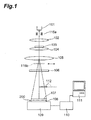
- this image pickup device As an example of such a conventional image pickup device, the image pickup device described in Japanese Patent Application Laid-Open No. 2000-324400 is known. As shown in Fig. 1, this image pickup device is equipped with a scintillator 107, a semiconductor substrate 109, a fiber optic plate 108 (referred to hereinafter as "FOP"), a CCD reading part control part 110, a computer 111, etc.
- the scintillator 107 emits light when illuminated by an electron beam.
- the semiconductor substrate 109 is positioned below scintillator 107 and has a CCD reading part for picking up a two-dimensional optical image.
- the FOP 108 is positioned between scintillator 107 and semiconductor substrate 109 and is optically coupled to semiconductor substrate 109 in order to carry an optical image to semiconductor substrate 109.
- the CCD reading part control part 110 controls a CCD reading part.
- the computer 111 converts image pickup data, taken in by the CCD reading part, into an image and displays the image resulting from conversion.
- 101 is an electron gun
- 102 is an irradiation lens system
- 103 is a sample
- 104 and 105 indicate an objective lens system
- 106 is a fluorescent plate
- 112 is an electron beam shielding plate
- 115a and 115b are electron beam shielding means
- 200 is an electron beam image pickup device, arranged from FOP 108 and semiconductor substrate 109.
- This invention has been made to resolve the above issue, and an object thereof is to provide an image pickup device, having a structure, with which electrostatic discharge is unlikely to occur during the joining of an FOP and a CCD reading part, and a method of manufacturing such an image pickup device.
- the image pickup device comprises a semiconductor substrate having a charge reading part (CCD reading part) constituted by a charge coupled device that detects incident light, and a fiber optic plate (FOP) having a light outgoing end surface to be optically coupled to the semiconductor substrate.
- the semiconductor substrate has a back surface, serving as a light-incident surface, and a front surface, opposing the back surface and being provided with the CCD reading part that detects light propagating from the back surface.
- the light outgoing end surface of the FOP is joined to the back surface of the semiconductor substrate.
- the light emitted from the FOP is transmitted through the semiconductor substrate from the back surface and thereafter reaches the CCD reading part disposed at the front surface.
- the light outgoing end surface of the FOP is joined to a part of the back surface of the semiconductor substrate that corresponds to a region of the front surface at which the CCD reading part is disposed. In this case, since the light outgoing end surface of the FOP overlaps the region at which the CCD reading part is formed while the semiconductor substrate is sandwiched in between, an optical image emitted from the FOP can be picked up without omission by the CCD reading part.
- the semiconductor substrate has a structure such that a recess is formed at a portion of the back surface corresponding to the region at which the CCD reading part is disposed and the thickness of the region at which the CCD reading part is disposed is thinner than the remaining region.
- a protective plate is preferably joined so as to cover the entirety of the CCD reading part.
- the image pickup device may comprise a semiconductor substrate, a package, an FOP, a cover, and electrical wirings.
- the semiconductor substrate has a back surface, serving as a light-incident surface, and a front surface, opposing the back surface and being provided with a CCD reading part constituted by a charge coupled device that detects light arriving from the back surface.
- This semiconductor substrate has a structure such that a recess is formed at a portion of the back surface corresponding to a region at which the CCD reading part is disposed and the thickness of the region at which the CCD reading part is disposed is thinner than the remaining region.
- the package has a cavity that houses the semiconductor substrate and that is fixed with the semiconductor substrate while the front surface of the semiconductor substrate faces a bottom part of the cavity.
- the FOP is housed at least in part in the cavity of the package and a light outgoing end surface thereof is joined to the back surface of the semiconductor substrate.
- the cover covers an upper opening of the cavity of the package. Also, this cover has a guiding opening for insertion of at least a part of the FOP into the cavity.
- the electrical wirings take out charge signals output from the CCD reading part to the exterior of the package.
- these electrical wirings include at least substrate electrodes, package-side wirings, and package-side electrodes.
- the substrate-side electrodes are disposed on the front surface of the semiconductor substrate.
- the package-side wirings are disposed on the cavity bottom surface and are electrically connected via bumps to the substrate-side electrodes.
- the package-side electrodes are disposed on an inner wall of the cavity and are electrically connected via bonding wires to the package-side wirings.
- the distance between the light outgoing end surface of the FOP and the CCD reading part is shortened and light of shorter wavelength can be detected at high sensitivity. Also, by the forming of the thin part, positioning in the process of joining the FOP to the semiconductor substrate is facilitated. In addition, since the electrical wirings for taking out the charge signals of the CCD reading part to the exterior can be shortened, the wiring capacity is made small and attenuation of the signal waveform will not occur.
- the image pickup device may comprise a semiconductor substrate, a package, an FOP, and electrical wirings.
- the semiconductor substrate has a back surface, serving as a light-incident surface, and a front surface, opposing the back surface and being provided with a CCD reading part constituted by a charge coupled device that detects light propagating from the back surface.
- This semiconductor substrate has a structure such that a recess is formed at a part of the back surface corresponding to a region at which the CCD reading part is disposed and the thickness of the region at which the CCD reading part is disposed is thinner than the remaining region.
- the package has a cavity which houses the semiconductor substrate, the cavity having one surface whose opening portion is covered by a bottom cover, and the other surface opposing the one surface and whose opening portion is attached with a guide member having a guiding opening.
- the semiconductor substrate is fixed to the package such that the CCD reading part and the bottom cover face each other while the semiconductor substrate is housed. At least a part of the FOP is housed inside the cavity of the package through the guiding opening. A light outgoing end surface of this FOP is joined to the region of the back surface of the semiconductor substrate that is thin in thickness.
- the electrical wirings take out charge signals output from the CCD reading part to the exterior of the package. In particular, these electrical wirings include at least substrate-side electrodes and package-side electrodes.
- the substrate-side electrodes are disposed on the front surface of the semiconductor substrate.
- the package-side electrodes are disposed on an inner wall of the package and are electrically connected via bonding wires to the substrate-side electrodes.
- the distance between the light outgoing end surface of the FOP and the CCD reading part is shortened and light of shorter wavelength can be detected at high sensitivity.
- a guiding opening is provided in the guide member that is mounted to the other opening portion of the package, and this guiding opening functions as a reference member in the process of inserting at least a part of the FOP inside the cavity and facilitates positioning in the process of joining the FOP to the semiconductor substrate.
- the wiring structure enables the electrical wirings for taking out the charge signals of the CCD reading part to the exterior of the package to be shortened, the wiring capacity is made small and attenuation of the signal waveform will not occur.
- a semiconductor substrate and an FOP are prepared, and a light outgoing end surface of the FOP is joined to a back surface of the semiconductor substrate.
- the semiconductor substrate has a back surface, serving as a light-incident surface, and a front surface, opposing the back surface and being provided with a CCD reading part constituted by a charge coupled device that detects light propagating from the back surface.
- the CCD reading part and the light outgoing end surface of the FOP do not contact each other directly in the step of joining the FOP and the semiconductor substrate, thereby preventing the flowing of excess current from the FOP to the CCD reading part. Electrostatic discharge of the CCD reading part is thus restrained and the manufacturing yield of the image pickup device is thus improved.
- a n image pickup device comprising a semiconductor substrate having a back surface, serving as a light-incident surface, and a front surface, opposing the back surface and being provided with a charge reading part constituted by a charge coupled device that detects light propagating from the back surface; and a fiber optic plate having a light outgoing end surface joined to the back surface of said semiconductor substrate.
- the light outgoing end surface of said fiber optic plate is joined to a part of the back surface of the semiconductor substrate that corresponds to a region at which said charge reading part is disposed.
- said semiconductor substrate has a structure such that the thickness of the region at which said charge reading part is disposed is made thinner than the thickness of the remaining region, and the light outgoing end surface of said fiber optic plate is joined to the part of said semiconductor substrate that is made thin in thickness.
- a protective plate is joined to the front surface of said semiconductor substrate so as to cover said charge reading part.
- an image pickup device comprising a semiconductor substrate having a back surface, serving as a light-incident surface, and a front surface, opposing the back surface and being provided with a charge reading part constituted by a charge coupled device that detects light propagating from the back surface, said semiconductor substrate having a structure such that the thickness of the region at which said charge reading part is disposed is made thinner than the thickness of the remaining region; a package having a cavity that houses said semiconductor substrate and that is fixed with said semiconductor substrate while the front surface of said semiconductor substrate faces a bottom part of said cavity; a fiber optic plate having a light outgoing end surface joined to the back surface of said semiconductor substrate while at least a part thereof is housed in said cavity of said package; a cover covering an upper opening of said cavity of said package, said cover having a guiding opening for inserting at least the part of said fiber optic plate into said cavity; and electrical wirings for taking out charge signals output from said charge reading part to the exterior of said package, said electrical wirings
- an image pickup device comprising a semiconductor substrate having a back surface, serving as a light-incident surface, and a front surface, opposing the back surface and being provided with a charge reading part constituted by a charge coupled device that detects light propagating from the back surface, said semiconductor substrate having a structure such that the thickness of the region at which said charge reading part is disposed is made thinner than the thickness of the remaining region; a package having a cavity that houses said semiconductor substrate and having one surf ace whose opening portion is covered by a bottom cover, and the other surface opposing said one surface and whose opening portion is attached with a guide member having a guiding opening, said package being fixed with said semiconductor substrate such that said charge reading part and said bottom cover face each other while said semiconductor substrate is housed; a fiber optic plate having at least a part housed in said cavity of said package via the guiding opening of said guide member, said fiber optic plate having a light outgoing end surface thereof being joined to the region of the back surface of said semiconductor
- a method of manufacturing an image pickup device comprising the steps of preparing a semiconductor substrate having a back surface, serving as a light-incident surface, and a front surface, opposing the back surface and being provided with a charge reading part constituted by a charge coupled device that detects light propagating from the back surface; preparing a fiber optic plate; and joining a light outgoing end surface of said fiber optic plate to the back surface of said semiconductor substrate.
- Fig. 1 is a diagram showing the structure of a transmission electron microscope that includes a conventional image pickup device
- Fig. 2 is a diagram showing the cross-sectional structure of a first embodiment of an image pickup device according to the present invention
- Figs. 3A to 3D are process diagrams for explaining a method of manufacturing the image pickup device according to the first embodiment (part 1);
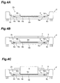
- Figs. 4A to 4C are process diagrams for explaining the method of manufacturing the image pickup device according to the first embodiment (part 2);
- Fig. 5 is a diagram showing the cross-sectional structure of a second embodiment of an image pickup device according to the present invention.
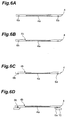
- Figs. 6A to 6D are process diagrams for explaining a method of manufacturing the image pickup device according to the second embodiment (part 1);
- Figs. 7A to 7D are process diagrams for explaining the method of manufacturing the image pickup device according to the second embodiment (part 2);
- Figs. 8A and 8B are process diagrams for explaining the method of manufacturing the image pickup device according to the second embodiment (part 3);
- Fig. 9 is a diagram showing the cross-sectional structure of a third embodiment of an image pickup device according to the present invention.
- Figs. 10A to 10D are process diagrams for explaining a method of manufacturing the image pickup device according to the third embodiment (part 1);
- Figs. 11A to 11D are process diagrams for explaining the method of manufacturing the image pickup device according to the third embodiment (part 2);
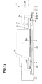
- Fig. 12 is a process diagrams for explaining the method of manufacturing the image pickup device according to the third embodiment (part 3).
- Fig. 2 is a diagram showing the cross-sectional structure of a first embodiment of an image pickup device according to the present invention.
- a semiconductor substrate 4 having a CCD reading part 4a is housed inside a cavity 2h of a package 2, and the semiconductor substrate 4 is optically coupled to an FOP 5.
- the image pickup device 1 comprises a package 2, having the cavity 2h surrounded by a bottom surface part 2a and the side wall parts 2b, a cover 3 covering an opening of package 2, the semiconductor substrate 4 comprised of silicon, etc. and having CCD reading part 4a formed on a front surface side, FOP 5 joined to the semiconductor substrate 4, and electrical wirings 6 for taking out charge signals output from the CCD reading part 4a to the exterior of the package 2.
- the cover 3 is formed with a guiding opening 3a for insertion of at least a part of the FOP 5 into the cavity 2h.
- the semiconductor substrate 4 has a thin part 4b formed therein by the thinning of a back surface region corresponding to a front surface region at which the CCD reading part 4a is disposed. Also, this semiconductor substrate 4 is fixed via bumps 6a to the bottom surface part 2a such that the CCD reading part 4a and the bottom surface part 2a face each other.
- the FOP 5 is inserted into the cavity 2h from the guiding opening 3a, and by a portion thereof being fitted onto the thin part 4b, a light outgoing end surface 5a of the FOP 5 becomes optically coupled to the thin part 4b.
- the electrical wirings 6 include substrate-side electrodes 6b disposed on the front surface of the semiconductor substrate 4, package-side wirings 6e disposed on the bottom surface part 2a, and package-side electrodes 6c disposed on steps 2c of the side wall parts 2b.
- the substrate-side electrodes 6b and the package-side wirings 6e are electrically connected via bumps 6a disposed on the substrate-side electrodes 6b by flip-chip bonding, and the package-side wirings 6e and the package-side electrodes 6c are electrically connected via bonding wires 6d (wire bonding).
- the principal parts of this image pickup device 1 correspond to electron image pickup device 200 of the transmission electron microscope shown in Fig. 1, and the light-incident end surface 5b of the FOP 5 is optically coupled to a scintillator, etc.
- the package 2 and the cover 3 are preferably formed of ceramic or other insulating material.
- the light outgoing end surface 5a of the FOP 5 and the thin part 4b of the semiconductor substrate 4 are preferably optically coupled by a room temperature curing type adhesive (silicone resin), etc., which is transparent to the emission wavelength of the scintillator.
- the thickness of the thin part 4b is preferably approximately 10 ⁇ m to 30 ⁇ m for increasing the sensitivity to light of short wavelength.
- the CCD reading part 4a preferably has the same planar shape as the light outgoing end surface 5a of the FOP 5 such that an optical image having propagated through the FOP 5 can be detected without omission.
- the light outgoing end surface 5a of the FOP 5 has a shape that is accurately fitted onto the thin part 4b, and at the back surface of the semiconductor substrate 4, the light outgoing end surface 5a is joined to the portion corresponding to the region at which the CCD reading part 4a is formed.
- the guiding opening 3a is an entrance for inserting a part of the FOP 5 into the cavity 2h, it has a size that is at least equal to or greater than the size of the light outgoing end surface 5a.
- the guide member 7, which is positioned the periphery of the guiding opening 3a is a member that defines the direction of insertion of the part of the FOP 5 into the cavity 2h and guides the light outgoing end surface 5a of the FOP 5 to the thin part 4b, the dimensional precision of the wall surfaces thereof is preferably no less than a predetermined value.
- the light outgoing end surface 5a of the FOP 5 has a size of 35. 7mm x 8.7mm and the guiding opening 3a has an opening size of 35.9mm x 8.9mm.
- the image pickup device 1 of this first embodiment has a structure such that the FOP 5 and the CCD reading part 4a do not contact each other directly, and thus even when excess current flows from the FOP 5 to the semiconductor substrate 4 in the process of joining the FOP 5 to the semiconductor substrate 4, electrostatic discharge of the CCD reading part 4a is restrained.
- the CCD reading part 4a can detect even light of short wavelength emitted from the light outgoing end surface 5a.
- the thin part 4b such that the light outgoing end surface 5a of the FOP 5 can be fitted in a gap-less manner, positioning in the process of joining the FOP 5 to the semiconductor substrate 4 is facilitated.
- the guide member 7 functions as a reference member in the insertion of at least a part of the FOP 5 into the cavity 2h, the FOP 5 can be inserted accurately onto the thin part 4b of the semiconductor substrate 4. Also, since the electrical wirings 6 for taking out charge signals of the CCD reading part 4a to the exterior are shortened, the electrical wirings 6 are made small in wiring capacity and the waveforms of signals from the CCD reading part 4a will not become attenuated.
- An electron beam is first made incident on the scintillator disposed at the light-incident end surface 5b side of the FOP 5.
- the light emitted from the scintillator then propagates through the FOP 5 from the light-incident end surface 5b to the light outgoing end surface 5a.
- the light that is emitted from the light outgoing end surface 5a of the FOP 5 passes through the thin part 4b from the back surface (surface on which the CCD reading part 4a is not formed) and reaches the CCD reading part 4a, disposed at the front surface side of the semiconductor substrate 4.
- the light that arrives at the CCD reading part 4a is photoelectrically converted and accumulated as charges in CCD reading part 4a.
- the accumulated charges are successively read based on the CCD control signals.
- the charge signals read from the CCD reading part 4a are converted into an image by a computer, etc.
- a method of manufacturing image pickup device 1 shall now be described using Figs. 3A to 3D and 4A to 4C.
- the thin part 4b is formed at the back surface of the region at which the CCD reading part 4a has been formed (Fig. 3B).
- the peripheral region is protected by a photoresist, etc., in a manner such that the portion that is to become the thin part 4b will be exposed, and by anisotropic etching, etc., the semiconductor substrate 4 is thinned from the back surface until the thickness of the thin part 4b becomes a predetermined thickness (10 ⁇ m to 30 ⁇ m).
- the bumps 6a formed of Au, are then formed on the substrate-side electrodes 6b of the semiconductor substrate 4 (Fig. 3C).
- the semiconductor substrate 4 is then set inside the ceramic package 2 such that the CCD reading part 4a and the bottom surface part 2a face each other, and by flip-chip bonding of the bumps 6a and the package-side wirings 6e, the semiconductor substrate 4 is fixed to the package 2 (Fig. 3D).
- the package-side wirings 6e and the package-side electrodes 6c disposed on the steps 2c of the side walls 2b, are electrically connected by bonding wires 6d (Fig. 4A). Thereafter, the cover 3, having a guide member 7 mounted at a predetermined position, is mounted onto the package 2 (Fig. 4B).
- the FOP 5 is inserted along the guide member 7 and into the interior of the package 2 through the guiding opening 3a formed in the cover 3.
- the outgoing end surface 5a of the FOP 5 is optically coupled to the thin part 4b (Fig. 4C).
- the gap between the FOP 5 and the guiding opening 3a is sealed by a resin, and thereby the image pickup device 1 of the first embodiment is obtained.
- the image pickup device 20 of this second embodiment has substantially the same structure as the above-described first embodiment, it differs in that a Peltier element 8, for cooling a CCD reading part 4a, is housed inside a cavity 2h of a package 2, a protective plate 9 is adhered onto a front surface (surface on which the CCD reading part 4a is formed) of a semiconductor substrate 4, a guide member 12 serves in common as the first embodiment's cover 3 (Fig. 2), etc.
- the principal parts of the image-pickup device 20 according to this second embodiment also correspond to the electron beam image pickup device 200 shown in Fig. 1 and can be applied to the transmission electron microscope of Fig. 1, etc.
- the image pickup device 20 comprises the package 2, the Peltier element 8, the semiconductor substrate 4, the protective plate 9, the bumps 6a, an auxiliary substrate 10, a resin 11, and the electrical wirings 6.
- the package 2 has the cavity 2h, surrounded by a bottom surface part 2a and side wall parts 2b.
- the Peltier element 8 is fixed to the bottom surface 2a in a state in which the bottom surface part 2a contacts a heat generating surface 8b.
- the semiconductor substrate 4 is positioned such that the front surface, on which the CCD reading part 4a is formed, faces a cooling surface 8a of the Peltier element 8.
- the protective plate 9 is adhered onto the front surface of the semiconductor substrate 4 so as to cover the region at which the CCD reading part 4a is formed.
- the bumps 6a are disposed at a peripheral part of the front surface.
- the auxiliary substrate 10 is a substrate, which is connected to the bumps 6a and is interposed between the bumps 6a and the cooling surface 8a, and is adhered to the vicinity of end part of cooling surface 8a.
- the resin 11 fills the space between the protective plate 9 and the cooling surface 8a.
- the electrical wirings 6 take out charge signals, output from the CCD reading part 4a, to the exterior of the package 2.
- the charge signals from the CCD reading part 4a are read via the substrate-side electrodes 6b, the bumps 6a, an electrical circuit formed on auxiliary substrate 10, and the bonding wires 6d, connecting the auxiliary substrate 10 to the package-side electrodes 6c, which are disposed on the steps 2c of the side wall parts 2b. Also, the gap between the auxiliary substrate 10 and the semiconductor substrate 4 is filled with a bump protection resin 13.
- the package 2 is preferably formed of ceramic or other insulating material.
- the light outgoing end surface 5a of the FOP 5 and the thin part 4b of the semiconductor substrate 4 are preferably optically coupled by a room temperature curing type adhesive (silicone resin), etc. , which is transparent to the emissionwavelength of the scintillator.
- the thickness of the thin part 4b is preferably approximately 10 ⁇ m to 30 ⁇ m for increasing the sensitivity to light of short wavelength.
- the CCD reading part 4a preferably has the same shape as the light outgoing end surface 5a of the FOP 5 such that an optical image having propagated through the FOP 5 can be detected without omission. Also, the light outgoing end surface 5a of the FOP 5 preferably has a shape that is accurately fitted onto the thin part 4b.
- the guiding opening 12a is a member that defines the direction of insertion of the FOP 5 into the interior of the package 2 and guides the light outgoing end surface 5a of the FOP 5 to the thin part 4b, the dimensional precision of the wall surfaces thereof is preferably no less than a predetermined value.
- the auxiliary substrate 10 is not restricted in particular in terms of material as long as it can support semiconductor substrate 4.
- a comparatively hard material such as silicon, glass, plastic, etc., is suited. Since the auxiliary substrate 10 has a function of transmitting the charge signals from the CCD reading part 4a to the bonding wires 6d, suitable electrical wirings are preferably disposed on a surface of the auxiliary substrate 10.
- the resin 11 for example, an epoxy resin is preferable for promoting the heat exchange between the cooling surface 8a of the Peltier element 8 and the CCD reading part 4a.
- the protective plate 9 is preferably formed, for example, of glass.
- the image pickup device 20 of this second embodiment has a structure such that the FOP 5 and the CCD reading part 4a do not contact each other directly. Thus, even when excess current flows from the FOP 5 to the semiconductor substrate 4 in the process of joining the FOP 5 to the semiconductor substrate 4, electrostatic discharge of the CCD reading part 4a is restrained.
- the CCD reading part 4a can detect even light of short wavelength emitted from the light outgoing end surface 5a.
- the thin part 4a By forming the thin part 4a such that the light outgoing end surface 5a of the FOP 5 can be fitted in a gap-less manner, positioning in the process of joining the FOP 5 to the semiconductor substrate 4 is facilitated.
- the guide member 12 functions as a reference member in the insertion of at least a part of the FOP 5 into the cavity 2h, the FOP 5 can be joined accurately to the thin part 4b of the semiconductor substrate 4. Also, since the protective plate 9, formed of glass, etc., is put in contact with the front surface of the semiconductor substrate 4, at which the CCD reading part 4a is formed, the CCD reading part 4a is protected from contamination, etc., and the semiconductor substrate is reinforced mechanically.
- the CCD reading part 4a is cooled by the Peltier element 8, the S/N ratio of the CCD reading part 4a is improved. Also, since the electrical wirings 6 for taking out charge signals of the CCD reading part 4a to the exterior are shortened, the electrical wirings 6 are made small in wiring capacity and the waveforms of signals from the CCD reading part 4a will not become attenuated.
- a method of manufacturing the image pickup device 20 of the second embodiment shall now be described using Figs. 6A to 6D, 7A to 7D and 8A and 8B.
- the thin part 4b is formed at the portion of the back surface corresponding to the region at which the CCD reading part 4a has been formed (Fig. 6B).
- the bumps 6a formed of Au, are then formed on the substrate-side electrodes 6b of the semiconductor substrate 4 (Fig. 6C).
- the semiconductor substrate 4 and the auxiliary substrate 10 are flip-chip bonded (Fig. 6D). Thereafter, in order to protect the bumps 6a, the gap between the semiconductor substrate 4 and the auxiliary substrate 10 is filled with silicone resin or other bump protection resin 13 (Fig. 7A).
- the protective plate 9 comprising a thin plate of glass, etc. is adhered, and the space formed by the auxiliary substrate 10 and the protective plate 9 is filled with resin 11 comprised of an epoxy resin, etc. (Fig. 7B).
- the auxiliary substrate 10 and the resin 11 are adhered, by means of an epoxy resin containing an Ag filler, etc. , onto the cooling surface 8a of the Peltier element 8, which has been mounted to the bottom surface part 2a of the package 2 (Fig. 7C).
- the semiconductor substrate 4 is thereby housed inside the cavity 2h.
- the auxiliary substrate 10 and the package-side electrodes 6c, disposed on the steps 2c of the side wall parts 2b, are then electrically connected by the bonding wires 6d comprised of Au (Fig. 7D).
- a room temperature curing type adhesive which is comprised of a silicone resin, etc. and has a property of being transparent to the light from the scintillator, is coated onto the thin part 4b of the semiconductor substrate 4 (Fig. 8A).
- a part of the FOP 5 is then inserted into the cavity 2h from the guiding opening 12a of the guide member 12, and the light outgoing end surface 5a of the FOP 5 is optically coupled to the thin part 4b (Fig. 8B).
- the image pickup device 20 of the second embodiment is obtained.
- the image pickup device 30 according to this third embodiment differs from the first embodiment in the shape of the package 2.
- the package 2 of this third embodiment has openings at two opposing surfaces.
- the opening portion formed on a bottom surface of the package 2 shall be referred to as “bottom surface opening 2g, " and the opening portion formed on an upper end surface of the package 2 shall be referred to as "top plate opening 2f.”
- the bottom surface opening 2g is covered by a bottom cover 2d, and a semiconductor substrate 4 is connected to this bottom cover 2d. That a protective plate 9 is put in contact with a front surface of the semiconductor substrate 4, at which a CCD reading part 4a is formed, is also a point of difference with respect to the first embodiment.
- the principal parts of the image-pickup device 30 according to this third embodiment also correspond to the electron beam image pickup device 200 shown in Fig. 1 and can be applied to the transmission electron microscope of Fig. 1, etc.
- the package 2 has the openings 2f and 2g at two surfaces that oppose each other. Put in another way, the package 2 is arranged from a top plate 2e and side wall parts 2b, and the bottom surface does not have a bottom but has the bottom surface opening 2g formed therein. Also, on the upper end surface of the package 2, the top plate 2e, having the top plate opening 2f formed in a central part thereof, is disposed.
- the bottom surface opening 2g of the package 2 is covered by a bottom cover 2d, and the semiconductor substrate 4, on the front surface side of which the CCD reading part 4a is formed, is housed inside the cavity of the package 2 by being fixed to the bottom cover 2d. Also, at least a part of the FOP 5 is inserted into the interior of the package 2 from the top plate opening 2f and joined to the semiconductor substrate 4.
- the image pickup device 30 further comprises electrical wirings 6 for taking out charge signals output from the CCD reading part 4a to the exterior of the package 2.
- a portion of a back surface that corresponds to the front surface region at which the CCD reading part 4a is formed is thinned (thin part 4b).
- the CCD reading part 4a is fixed to the bottom cover 2d via a protective plate 9 so as to face the bottom cover 2d, and a spacer 14, having an opening that surrounds the periphery of the top plate opening 2f, is positioned between the semiconductor substrate 4 and the top plate 2e.
- a guide member 7, having a guiding opening 7a, is mounted to the top plate opening 2f of the package 2, and at least a part of the FOP 5 is inserted into the package 2 fromthis guiding opening 7a and a light outgoing end surface 5a thereof is optically coupled to the thin part 4b.
- the electrical wirings 6 include substrate-side electrodes 6b disposed on the front surface of the semiconductor substrate 4, and package-side electrodes 6c disposed on the steps 2c of the side wall parts 2b, and these substrate-side electrodes 6b and package-side electrodes 6c are electrically connected via bonding wires 6d.
- the image pickup device 30 has a structure such that the FOP 5 and the CCD reading part 4a do not contact each other directly. Thus, even when excess current flows from the FOP 5 to the semiconductor substrate 4 in the process of joining the FOP 5 to the semiconductor substrate 4, electrostatic discharge of the CCD reading part 4a is restrained.
- the CCD reading part 4a can detect even light of short wavelength emitted from the light outgoing end surface 5a.
- the thin part 4a By forming the thin part 4a such that the light outgoing end surface 5a of the FOP 5 can be fitted in a gap-less manner, positioning in the process of joining the FOP 5 to the semiconductor substrate 4 is facilitated.
- the protective plate 9, comprised of glass, etc. is put in contact with the front surface of the semiconductor substrate 4, at which the CCD reading part 4a is formed, the CCD reading part 4a is protected from contamination, etc., and the semiconductor substrate is reinforced mechanically.
- the electrical wirings 6 for taking out charge signals of the CCD reading part 4a to the exterior are shortened, the electrical wirings 6 are made small in wiring capacity and the waveforms of signals from the CCD reading part 4a will not become attenuated.
- the spacer 14 is positioned between the back surface of the semiconductor substrate 4 and the top plate 2e of the package 2, the interval between the two is kept constant.
- a method of manufacturing image pickup device 30 according to the third embodiment shall now be described using Figs. 10A to 10D, 11A to 11D and 12.
- the thin part 4b is formed at the portion of the back surface corresponding to the front surface region at which the CCD reading part 4a has been formed (Fig. 10B).
- the ceramic spacer 14, for fixing the semiconductor substrate 4 is then adhered onto the top plate 2e of the package 2 by an epoxy resin containing Ag filler, etc. (Fig. 10C).
- the semiconductor substrate 4 is adhered, with the CCD reading part 4a faced downwards, onto the spacer 14 by an epoxy resin containing Ag filler, etc. (Fig. 10D). Thereafter, the protective plate 9, which is a thin plate of glass, etc., is adhered by an epoxy resin, etc., onto the front surface of the semiconductor substrate 4 so as to cover the region at which the CCD reading part 4a has been formed (Fig. 11A).
- the bottom cover 2d comprised of ceramic, is adhered onto the package 2 and the protective plate 9 by means of a room temperature curing type adhesive agent, which is comprised of a silicone resin, etc. (Fig. 11C).
- the bottom cover 2d and the protective plate 9 are thereby put in a state enabling conduction of heat and it becomes possible to cool the CCD reading part 4a via the bottom cover 2d.
- a room temperature curing type adhesive agent which is comprised of a silicone resin, etc. , is coated onto the thin part 4b, and the guide member 7, which functions as a positioning member in the process of inserting a part of the FOP 5 into the package 2, is mounted to the opening 2f provided in the top plate 2e (Fig. 11D).
- the FOP 5 is then inserted into the package 2 from the guiding opening 7a of the guide member 7, and the light outgoing end surface 5a of the FOP 5 is optically coupled to the thin part 4b (Fig. 12). Thereafter, the gap between the FOP 5 and the guiding opening 7a is sealed by a resin, and the image pickup device 30 of the third embodiment is thus obtained.
- the image pickup device having a structure with which a CCD reading part is unlikely to undergo electrostatic discharge in the process of joining an FOP to the CCD reading part, and a method of manufacturing such an image pickup device are provided. Also, since the thickness of a semiconductor substrate of a thin part, to which the FOP is joined, is only approximately 10 ⁇ m to 30 ⁇ m, the CCD reading part can detect even light of short wavelength that is emitted from a light outgoing end surface. By forming the thin part of the semiconductor substrate so that the light outgoing end surface of the FOP can be fitted on without looseness, positioning in the process of joining the FOP to the semiconductor substrate is facilitated.
Landscapes
- Engineering & Computer Science (AREA)
- Multimedia (AREA)
- Signal Processing (AREA)
- Chemical & Material Sciences (AREA)
- Analytical Chemistry (AREA)
- Solid State Image Pick-Up Elements (AREA)
- Transforming Light Signals Into Electric Signals (AREA)
- Measurement Of Radiation (AREA)
Applications Claiming Priority (2)
| Application Number | Priority Date | Filing Date | Title |
|---|---|---|---|
| JP2002296543A JP4227389B2 (ja) | 2002-10-09 | 2002-10-09 | 撮像装置及びその製造方法 |
| EP03754041A EP1557885B1 (fr) | 2002-10-09 | 2003-10-08 | Dispositif de saisie d'image |
Related Parent Applications (1)
| Application Number | Title | Priority Date | Filing Date |
|---|---|---|---|
| EP03754041A Division EP1557885B1 (fr) | 2002-10-09 | 2003-10-08 | Dispositif de saisie d'image |
Publications (3)
| Publication Number | Publication Date |
|---|---|
| EP1883111A2 true EP1883111A2 (fr) | 2008-01-30 |
| EP1883111A3 EP1883111A3 (fr) | 2008-12-10 |
| EP1883111B1 EP1883111B1 (fr) | 2015-04-22 |
Family
ID=32089240
Family Applications (2)
| Application Number | Title | Priority Date | Filing Date |
|---|---|---|---|
| EP03754041A Expired - Lifetime EP1557885B1 (fr) | 2002-10-09 | 2003-10-08 | Dispositif de saisie d'image |
| EP20070019811 Expired - Lifetime EP1883111B1 (fr) | 2002-10-09 | 2003-10-08 | Dispositif de capture d'images |
Family Applications Before (1)
| Application Number | Title | Priority Date | Filing Date |
|---|---|---|---|
| EP03754041A Expired - Lifetime EP1557885B1 (fr) | 2002-10-09 | 2003-10-08 | Dispositif de saisie d'image |
Country Status (7)
| Country | Link |
|---|---|
| US (1) | US7550811B2 (fr) |
| EP (2) | EP1557885B1 (fr) |
| JP (1) | JP4227389B2 (fr) |
| CN (1) | CN100409446C (fr) |
| AU (1) | AU2003272948A1 (fr) |
| DE (1) | DE60335283D1 (fr) |
| WO (1) | WO2004034471A1 (fr) |
Families Citing this family (19)
| Publication number | Priority date | Publication date | Assignee | Title |
|---|---|---|---|---|
| NZ571803A (en) * | 2006-04-07 | 2011-12-22 | Vertex Pharma | Amide indole derivatives as modulators of ATP-binding cassette transporters |
| KR100800476B1 (ko) * | 2006-07-11 | 2008-02-04 | 삼성전자주식회사 | 반도체 패키지 및 그 제조방법과 반도체 모듈 및 그제조방법 |
| US7675131B2 (en) * | 2007-04-05 | 2010-03-09 | Micron Technology, Inc. | Flip-chip image sensor packages and methods of fabricating the same |
| DE102008001675A1 (de) * | 2008-05-09 | 2009-11-12 | Robert Bosch Gmbh | Kameramodul mit verbessertem Kühlkonzept |
| JP2010093752A (ja) * | 2008-10-10 | 2010-04-22 | Sony Corp | 固体撮像素子及び信号処理システム |
| JP2010093754A (ja) * | 2008-10-10 | 2010-04-22 | Sony Corp | 固体撮像素子及び信号処理システム |
| DE102009009602A1 (de) * | 2008-10-27 | 2010-04-29 | Ifg - Institute For Scientific Instruments Gmbh | Spektralauflösende elektronische Röntgenkamera |
| JP5464133B2 (ja) * | 2010-11-29 | 2014-04-09 | 株式会社島津製作所 | 撮像装置の製造方法 |
| EP2487703A1 (fr) | 2011-02-14 | 2012-08-15 | Fei Company | Détecteur pour la microscopie à particules chargées |
| JP5940887B2 (ja) * | 2012-05-18 | 2016-06-29 | 浜松ホトニクス株式会社 | 固体撮像装置 |
| US9046426B1 (en) * | 2012-06-15 | 2015-06-02 | The United States Of America As Represented By The Administrator Of National Aeronautics And Space Administration | Modular apparatus and method for attaching multiple devices |
| JP6083554B2 (ja) * | 2012-08-07 | 2017-02-22 | 国立大学法人静岡大学 | 撮像モジュール |
| JP5600722B2 (ja) * | 2012-11-02 | 2014-10-01 | 株式会社堀場製作所 | 放射線検出器、放射線検出装置、及びx線分析装置 |
| JP6300442B2 (ja) * | 2013-01-18 | 2018-03-28 | オリンパス株式会社 | 光伝送モジュールおよび撮像装置 |
| JP2015096882A (ja) * | 2013-11-15 | 2015-05-21 | セイコーエプソン株式会社 | 電気光学装置および投射型表示装置 |
| EP3120383B1 (fr) * | 2015-01-15 | 2017-11-29 | Koninklijke Philips N.V. | Ensemble de module détecteur d'imagerie |
| JP7686365B2 (ja) | 2018-11-20 | 2025-06-02 | キヤノン株式会社 | 電子部品および機器 |
| US11355659B2 (en) * | 2019-11-27 | 2022-06-07 | Xintec Inc. | Chip package and manufacturing method thereof |
| CN114730780A (zh) * | 2019-12-27 | 2022-07-08 | 索尼半导体解决方案公司 | 传感器装置 |
Citations (2)
| Publication number | Priority date | Publication date | Assignee | Title |
|---|---|---|---|---|
| JPS62189883A (ja) | 1986-02-17 | 1987-08-19 | Matsushita Electronics Corp | 固体撮像装置 |
| JP2000324400A (ja) | 1999-05-13 | 2000-11-24 | Hitachi Ltd | 電子線像撮像装置及び電子顕微鏡 |
Family Cites Families (6)
| Publication number | Priority date | Publication date | Assignee | Title |
|---|---|---|---|---|
| US4760031A (en) * | 1986-03-03 | 1988-07-26 | California Institute Of Technology | Producing CCD imaging sensor with flashed backside metal film |
| JPH06196680A (ja) * | 1992-12-22 | 1994-07-15 | Hamamatsu Photonics Kk | 半導体エネルギー検出器とその製造方法 |
| JPH09199699A (ja) * | 1996-01-12 | 1997-07-31 | Hitachi Ltd | 薄膜イメージセンサ |
| JPH11188033A (ja) | 1997-12-26 | 1999-07-13 | Hamamatsu Photonics Kk | 歯科用x線像撮像装置および歯科用x線像撮像装置用モジュール |
| JP4005704B2 (ja) | 1998-07-14 | 2007-11-14 | 浜松ホトニクス株式会社 | X線パネルセンサ |
| JP4562875B2 (ja) | 2000-07-17 | 2010-10-13 | 浜松ホトニクス株式会社 | 半導体装置 |
-
2002
- 2002-10-09 JP JP2002296543A patent/JP4227389B2/ja not_active Expired - Lifetime
-
2003
- 2003-10-08 EP EP03754041A patent/EP1557885B1/fr not_active Expired - Lifetime
- 2003-10-08 CN CNB2003801006541A patent/CN100409446C/zh not_active Expired - Lifetime
- 2003-10-08 WO PCT/JP2003/012911 patent/WO2004034471A1/fr not_active Ceased
- 2003-10-08 US US10/530,754 patent/US7550811B2/en not_active Expired - Lifetime
- 2003-10-08 DE DE60335283T patent/DE60335283D1/de not_active Expired - Lifetime
- 2003-10-08 AU AU2003272948A patent/AU2003272948A1/en not_active Abandoned
- 2003-10-08 EP EP20070019811 patent/EP1883111B1/fr not_active Expired - Lifetime
Patent Citations (2)
| Publication number | Priority date | Publication date | Assignee | Title |
|---|---|---|---|---|
| JPS62189883A (ja) | 1986-02-17 | 1987-08-19 | Matsushita Electronics Corp | 固体撮像装置 |
| JP2000324400A (ja) | 1999-05-13 | 2000-11-24 | Hitachi Ltd | 電子線像撮像装置及び電子顕微鏡 |
Non-Patent Citations (1)
| Title |
|---|
| GRUNER S.M. ET AL.: "Charge-coupled device area x-ray detectors", REVIEW OF SCIENTIFIC INSTRUMENTS, vol. 73, no. 8, pages 2815 - 2842 |
Also Published As
| Publication number | Publication date |
|---|---|
| EP1557885B1 (fr) | 2010-12-08 |
| AU2003272948A1 (en) | 2004-05-04 |
| WO2004034471A1 (fr) | 2004-04-22 |
| DE60335283D1 (de) | 2011-01-20 |
| US20060240586A1 (en) | 2006-10-26 |
| EP1557885A4 (fr) | 2005-12-28 |
| CN1692498A (zh) | 2005-11-02 |
| EP1883111B1 (fr) | 2015-04-22 |
| US7550811B2 (en) | 2009-06-23 |
| CN100409446C (zh) | 2008-08-06 |
| JP2004134527A (ja) | 2004-04-30 |
| EP1883111A3 (fr) | 2008-12-10 |
| JP4227389B2 (ja) | 2009-02-18 |
| EP1557885A1 (fr) | 2005-07-27 |
Similar Documents
| Publication | Publication Date | Title |
|---|---|---|
| US7550811B2 (en) | Image pickup device and method of manufacturing the same | |
| CN100382346C (zh) | 光半导体器件及采用该器件的电子装置 | |
| US6784409B2 (en) | Electronic device with encapsulant of photo-set resin and production process of same | |
| US5418566A (en) | Compact imaging apparatus for electronic endoscope with improved optical characteristics | |
| US6915049B2 (en) | Optical module and method of manufacturing the same, and optical transmission device | |
| US7961989B2 (en) | Optical chassis, camera having an optical chassis, and associated methods | |
| US20140168510A1 (en) | Imaging element module and method for manufacturing the same | |
| JP2003503858A (ja) | 光子デバイス用気密形チップスケールパッケージ | |
| EP2355489B1 (fr) | Module d'appareil photo | |
| KR20050026491A (ko) | 카메라 모듈, 카메라 모듈용 홀더, 카메라 시스템 및카메라 모듈 제조 방법 | |
| CN114946038A (zh) | 光电转换模块 | |
| JPS61112480A (ja) | 一体化撮像器―プリズム構体 | |
| WO2023032260A1 (fr) | Dispositif à semi-conducteurs et équipement électronique | |
| CN100466271C (zh) | 半导体装置 | |
| US7476036B2 (en) | Optocoupler for converting optical signals into electrical signals and vice versa | |
| US20010022370A1 (en) | Transducer module with an optical semiconductor, and method for producing a transducer module | |
| KR101109278B1 (ko) | 고체 촬상 장치 | |
| US20050237419A1 (en) | Camera module, holder for use in a camera module, camera system and method of manufacturing a camera module | |
| US7612442B2 (en) | Semiconductor device | |
| JPH0846224A (ja) | オプトエレクトロニック組立体及びその製造方法及び使用方法 | |
| EP0475370A2 (fr) | Appareil compact de formation d'images avec des caractéristiques optiques améliorées pour des endoscopes électroniques | |
| JP2010050725A (ja) | 撮像ユニット、撮像ユニットの製造方法および撮像装置 | |
| CN104303303B (zh) | 固体摄像装置 | |
| JP2025047809A (ja) | 電子部品および機器 | |
| JPH0777411B2 (ja) | 固体撮像装置 |
Legal Events
| Date | Code | Title | Description |
|---|---|---|---|
| PUAI | Public reference made under article 153(3) epc to a published international application that has entered the european phase |
Free format text: ORIGINAL CODE: 0009012 |
|
| 17P | Request for examination filed |
Effective date: 20071010 |
|
| AC | Divisional application: reference to earlier application |
Ref document number: 1557885 Country of ref document: EP Kind code of ref document: P |
|
| AK | Designated contracting states |
Kind code of ref document: A2 Designated state(s): DE FR GB |
|
| PUAL | Search report despatched |
Free format text: ORIGINAL CODE: 0009013 |
|
| AK | Designated contracting states |
Kind code of ref document: A3 Designated state(s): DE FR GB |
|
| 17Q | First examination report despatched |
Effective date: 20090421 |
|
| AKX | Designation fees paid |
Designated state(s): DE FR GB |
|
| RIC1 | Information provided on ipc code assigned before grant |
Ipc: H01L 27/148 20060101ALI20141001BHEP Ipc: H01L 31/0203 20140101ALI20141001BHEP Ipc: H01J 37/244 20060101ALI20141001BHEP Ipc: H04N 5/225 20060101ALI20141001BHEP Ipc: H01J 37/26 20060101ALI20141001BHEP Ipc: H01L 27/146 20060101AFI20141001BHEP Ipc: G01T 1/20 20060101ALI20141001BHEP Ipc: H01J 37/22 20060101ALI20141001BHEP |
|
| GRAP | Despatch of communication of intention to grant a patent |
Free format text: ORIGINAL CODE: EPIDOSNIGR1 |
|
| INTG | Intention to grant announced |
Effective date: 20141106 |
|
| GRAS | Grant fee paid |
Free format text: ORIGINAL CODE: EPIDOSNIGR3 |
|
| GRAA | (expected) grant |
Free format text: ORIGINAL CODE: 0009210 |
|
| AC | Divisional application: reference to earlier application |
Ref document number: 1557885 Country of ref document: EP Kind code of ref document: P |
|
| AK | Designated contracting states |
Kind code of ref document: B1 Designated state(s): DE FR GB |
|
| REG | Reference to a national code |
Ref country code: GB Ref legal event code: FG4D |
|
| REG | Reference to a national code |
Ref country code: DE Ref legal event code: R096 Ref document number: 60347549 Country of ref document: DE Effective date: 20150603 |
|
| REG | Reference to a national code |
Ref country code: FR Ref legal event code: PLFP Year of fee payment: 13 |
|
| REG | Reference to a national code |
Ref country code: DE Ref legal event code: R097 Ref document number: 60347549 Country of ref document: DE |
|
| PLBE | No opposition filed within time limit |
Free format text: ORIGINAL CODE: 0009261 |
|
| STAA | Information on the status of an ep patent application or granted ep patent |
Free format text: STATUS: NO OPPOSITION FILED WITHIN TIME LIMIT |
|
| 26N | No opposition filed |
Effective date: 20160125 |
|
| REG | Reference to a national code |
Ref country code: FR Ref legal event code: PLFP Year of fee payment: 14 |
|
| REG | Reference to a national code |
Ref country code: FR Ref legal event code: PLFP Year of fee payment: 15 |
|
| REG | Reference to a national code |
Ref country code: FR Ref legal event code: PLFP Year of fee payment: 16 |
|
| PGFP | Annual fee paid to national office [announced via postgrant information from national office to epo] |
Ref country code: GB Payment date: 20220901 Year of fee payment: 20 |
|
| PGFP | Annual fee paid to national office [announced via postgrant information from national office to epo] |
Ref country code: FR Payment date: 20220908 Year of fee payment: 20 |
|
| PGFP | Annual fee paid to national office [announced via postgrant information from national office to epo] |
Ref country code: DE Payment date: 20220621 Year of fee payment: 20 |
|
| P01 | Opt-out of the competence of the unified patent court (upc) registered |
Effective date: 20230517 |
|
| REG | Reference to a national code |
Ref country code: DE Ref legal event code: R071 Ref document number: 60347549 Country of ref document: DE |
|
| REG | Reference to a national code |
Ref country code: GB Ref legal event code: PE20 Expiry date: 20231007 |
|
| PG25 | Lapsed in a contracting state [announced via postgrant information from national office to epo] |
Ref country code: GB Free format text: LAPSE BECAUSE OF EXPIRATION OF PROTECTION Effective date: 20231007 |
|
| PG25 | Lapsed in a contracting state [announced via postgrant information from national office to epo] |
Ref country code: GB Free format text: LAPSE BECAUSE OF EXPIRATION OF PROTECTION Effective date: 20231007 |