EP1886407B1 - Detecteur gfsk/gmsk a rendement ameliore en matiere de brouillage dans la meme voie et dans les voies awgn - Google Patents
Detecteur gfsk/gmsk a rendement ameliore en matiere de brouillage dans la meme voie et dans les voies awgn Download PDFInfo
- Publication number
- EP1886407B1 EP1886407B1 EP06760585A EP06760585A EP1886407B1 EP 1886407 B1 EP1886407 B1 EP 1886407B1 EP 06760585 A EP06760585 A EP 06760585A EP 06760585 A EP06760585 A EP 06760585A EP 1886407 B1 EP1886407 B1 EP 1886407B1
- Authority
- EP
- European Patent Office
- Prior art keywords
- signal
- feedback
- detector
- phase
- detected
- Prior art date
- Legal status (The legal status is an assumption and is not a legal conclusion. Google has not performed a legal analysis and makes no representation as to the accuracy of the status listed.)
- Ceased
Links
- 238000001914 filtration Methods 0.000 claims description 7
- 238000000034 method Methods 0.000 claims description 7
- 239000000654 additive Substances 0.000 claims description 4
- 230000000996 additive effect Effects 0.000 claims description 4
- 238000001514 detection method Methods 0.000 abstract description 8
- 230000035945 sensitivity Effects 0.000 abstract description 7
- 230000002411 adverse Effects 0.000 abstract description 3
- 238000006243 chemical reaction Methods 0.000 description 9
- 238000010586 diagram Methods 0.000 description 4
- 238000005070 sampling Methods 0.000 description 3
- 239000002243 precursor Substances 0.000 description 2
- 238000007476 Maximum Likelihood Methods 0.000 description 1
- 230000003190 augmentative effect Effects 0.000 description 1
- 238000011144 upstream manufacturing Methods 0.000 description 1
Images


Classifications
-
- H—ELECTRICITY
- H04—ELECTRIC COMMUNICATION TECHNIQUE
- H04L—TRANSMISSION OF DIGITAL INFORMATION, e.g. TELEGRAPHIC COMMUNICATION
- H04L27/00—Modulated-carrier systems
- H04L27/18—Phase-modulated carrier systems, i.e. using phase-shift keying
- H04L27/22—Demodulator circuits; Receiver circuits
- H04L27/233—Demodulator circuits; Receiver circuits using non-coherent demodulation
- H04L27/2331—Demodulator circuits; Receiver circuits using non-coherent demodulation wherein the received signal is demodulated using one or more delayed versions of itself
-
- H—ELECTRICITY
- H04—ELECTRIC COMMUNICATION TECHNIQUE
- H04L—TRANSMISSION OF DIGITAL INFORMATION, e.g. TELEGRAPHIC COMMUNICATION
- H04L27/00—Modulated-carrier systems
- H04L27/10—Frequency-modulated carrier systems, i.e. using frequency-shift keying
-
- H—ELECTRICITY
- H04—ELECTRIC COMMUNICATION TECHNIQUE
- H04L—TRANSMISSION OF DIGITAL INFORMATION, e.g. TELEGRAPHIC COMMUNICATION
- H04L25/00—Baseband systems
- H04L25/02—Details ; arrangements for supplying electrical power along data transmission lines
- H04L25/03—Shaping networks in transmitter or receiver, e.g. adaptive shaping networks
- H04L25/03006—Arrangements for removing intersymbol interference
- H04L25/03012—Arrangements for removing intersymbol interference operating in the time domain
- H04L25/03114—Arrangements for removing intersymbol interference operating in the time domain non-adaptive, i.e. not adjustable, manually adjustable, or adjustable only during the reception of special signals
- H04L25/03127—Arrangements for removing intersymbol interference operating in the time domain non-adaptive, i.e. not adjustable, manually adjustable, or adjustable only during the reception of special signals using only passive components
-
- H—ELECTRICITY
- H04—ELECTRIC COMMUNICATION TECHNIQUE
- H04L—TRANSMISSION OF DIGITAL INFORMATION, e.g. TELEGRAPHIC COMMUNICATION
- H04L25/00—Baseband systems
- H04L25/02—Details ; arrangements for supplying electrical power along data transmission lines
- H04L25/03—Shaping networks in transmitter or receiver, e.g. adaptive shaping networks
- H04L25/03006—Arrangements for removing intersymbol interference
- H04L25/03012—Arrangements for removing intersymbol interference operating in the time domain
- H04L25/03114—Arrangements for removing intersymbol interference operating in the time domain non-adaptive, i.e. not adjustable, manually adjustable, or adjustable only during the reception of special signals
- H04L25/03133—Arrangements for removing intersymbol interference operating in the time domain non-adaptive, i.e. not adjustable, manually adjustable, or adjustable only during the reception of special signals with a non-recursive structure
-
- H—ELECTRICITY
- H04—ELECTRIC COMMUNICATION TECHNIQUE
- H04L—TRANSMISSION OF DIGITAL INFORMATION, e.g. TELEGRAPHIC COMMUNICATION
- H04L27/00—Modulated-carrier systems
- H04L27/18—Phase-modulated carrier systems, i.e. using phase-shift keying
-
- H—ELECTRICITY
- H04—ELECTRIC COMMUNICATION TECHNIQUE
- H04L—TRANSMISSION OF DIGITAL INFORMATION, e.g. TELEGRAPHIC COMMUNICATION
- H04L27/00—Modulated-carrier systems
- H04L27/18—Phase-modulated carrier systems, i.e. using phase-shift keying
- H04L27/20—Modulator circuits; Transmitter circuits
- H04L27/2003—Modulator circuits; Transmitter circuits for continuous phase modulation
- H04L27/2007—Modulator circuits; Transmitter circuits for continuous phase modulation in which the phase change within each symbol period is constrained
- H04L27/2017—Modulator circuits; Transmitter circuits for continuous phase modulation in which the phase change within each symbol period is constrained in which the phase changes are non-linear, e.g. generalized and Gaussian minimum shift keying, tamed frequency modulation
Definitions
- the invention relates to a detector within a demodulation system for a wireless receiver that may provide enhanced performance with respect to both additive white Gaussian noise and co-channel interference, and may enable the sensitivity of the detector to be adjustably configured.
- the performance of a receiver with respect to additive white Gaussian noise may be related to a sensitivity of the receiver.
- the sensitivity of the receiver may also be related to a performance of the receiver with respect to co-channel interference.
- the performance with respect to AWGN may be at least partially a function of a demodulation scheme.
- the performance with respect to co-channel interference may be at least partially a function of the demodulation scheme and an inter symbol interference (“ISI").
- ISI inter symbol interference
- pursuing an enhanced performance with respect to AWGN may degrade performance with respect to co-channel interference and vice versa.
- MLSE Maximum Likelihood Sequence Detection
- MLSE may not be utilized in a system with a variable modulation index, and MLSE implementation may be complex and costly, which may marginalize its employment in lower cost systems.
- DFE Decision Feedback Equalization
- a demodulation system including a detector that may enhance performance with respect to AWGN and/or co-channel interference at a reasonable cost of implementation. Additionally, there may be a need for a demodulation system including a detector that may allow the sensitivity of the detector to be configured or reconfigured according to a current application.
- One aspect of the invention may be related to a detector for detecting a received signal according to a Gaussian shift keying ("GPSK/GMSK") modulation scheme.
- the detector may enhance a detection performance of the receiver while limiting one or more implementation impacts.
- An implementation impact may include an implementation complexity impact, an implementation cost impact, or other impacts.
- the detection performance of the detector may be enhanced in relation to one or more performance aspects, such as, an ISI aspect, an AWGN aspect, a co-channel interference aspect, a sensitivity aspect, an error propagation aspect, or other aspects.
- the detector may be configured or reconfigured to enhance one or more particular performance aspects.
- the enhancement of the particular performance aspects may affect, adversely or otherwise, one or more related performance aspects that may be related to the particular performance aspects.
- the detector may be configured or reconfigured according to a current application of the detector.
- An application of the detector may include a voice application, a data application, a long-range application, a short-range application, or other applications.
- a receiver that employs AGC without a differential phase detector is known from US 2002061738A1 .
- the detector may acquire a received signal that may represent a string of symbols.
- the received signal may include an / component and a Q component.
- the detector may convert the received signal to a phase signal.
- the phase signal may be related to a phase differential between consecutive symbols in the received signal.
- the phase signal may be received by an equalizer.
- the equalizer may filter interference, such as ISI, or other interference, from the phase signal. By filtering interference from the phase signal, the equalizer may generate a filtered phase signal.
- the filtered phase signal may be received by a decision feedback data slicer.
- the decision feedback data slicer may combine the filtered phase signal with a feedback signal to generate a combined signal.
- the combined signal may be converted to a detected signal
- the decision feedback data slicer may include a feedback portion that generates the feedback signal.
- the feedback portion may include a configurable feedback gain section that may provide the feedback signal with a configurable gain.
- the configurable feedback gain section may permit a detection performance of the detector to be enhanced according to one or more performance aspects.
- the configurable feedback gain section may be configured or reconfigured via an operative link to a feedback gain Interface.
- the detector may include an equalizer.
- the equalizer may filter interference from a phase signal. Filtering interference from the phase signal may generate a filtered phase signal.
- the equalizer may be provided in the detector such that the equalizer does not create a risk of error propagation.
- the equalizer may be provided to filter pre-cursor interference.
- the equalizer may include a filter, such as an FIR filter, or other filter.
- One or more filter features of the equalizer may be selected according to one or more performance aspects, received signal aspects, implementation impacts, and/or other aspects.
- a filter feature may include, a tap number feature, a sampling rate feature, a tape coefficient feature, or other feature.
- the detector may include a decision feedback data slicer.
- the decision feedback data slicer may include a feedback combination section.
- the feedback combination section may combine the filtered phase signal with a feedback signal to generate a combined signal.
- the feedback combination section may include an adder, a summer, a multiplier, an averager, or other combination sections.
- the decision feedback data slicer may include a limiter.
- the limiter may perform one or more conversions on the combined signal to generate a preliminary detected signal.
- a conversion may include a conversion to a purely binary signal wherein each symbol in a symbol string associated with the phase signal may be represented as a single binary symbol, such as, a 1 , a 0 , a high, a low, or another binary symbol, or other conversions.
- the decision feedback data slicer may include a detected signal delay section.
- the detected signal delay section may delay the preliminary detected signal to generate a detected signal.
- the decision feedback data slicer may include a feedback portion.
- the feedback portion may include a detected feedback gain section.
- the detected feedback gain section may receive the detected signal and may generate a detected feedback signal corresponding to the detected signal.
- the feedback portion may include a filtered phase feedback signal delay section.
- the filtered phase feedback delay section may delay the filtered phase signal to generate a filtered phase feedback signal.
- the feedback portion may include a preliminary feedback combination section.
- the preliminary feedback combination section may combine two or more component feedback signals to generate a preliminary feedback signal.
- a component feedback signal may include the detected feedback signal, the filtered phase feedback signal, or other component feedback signals.
- the preliminary feedback combination section may include an adder, a summer, a multiplier, an averager, or other combination sections.
- the feedback portion may include a configurable feedback gain section.
- the configurable feedback gain section may provide the preliminary feedback signal with a configurable gain to generate the feedback signal.
- the configurable feedback gain section may permit a detection performance of the detector to be enhanced according to one or more performance aspects.
- the configurable feedback gain section may be configured or reconfigured via an operative link to a feedback gain Interface.
- a GFSK receiver that does not incorporate gain control is known from EP 0 866 567 A2 .
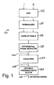
- FIG. 1 illustrates an exemplary embodiment of a detector 110 for detecting a received signal according to a GFSK/GMSK modulation scheme.
- the received signal may represent a string of symbols.
- the received signal may include an I component and a Q component.
- the received signal may be fed through one or more analog-to-digital converters ("ADC") 112.
- ADC 112 may digitally quantify the / and Q components of the received signal.
- the quantified / and Q components may then be normalized by a normalizer 114.
- the normalized / and Q components may then be converted to a phase value. This conversion may take place in a look-up table 116.
- Look-up table 116 may include an arctangent ROM table, or other look up tables.
- the detector may include a differential phase detector 118. Differential phase detector 118 may convert the phase values generated by look-up table 116 into a phase signal 120 associated with the phase differential between consecutive symbols In the symbol string represented by the received signal.
- phase signal 120 may be received by an equalizer 122.
- Equalizer 122 may filter interference, such as ISI, or other interference, from phase signal 120. By filtering interference from phase signal 120, equalizer 122 may generate a filtered phase signal 124. Filtered phase signal 124 may be received by a decision feedback data slicer 126. Decision feedback data slicer 126 may generate a detected signal 128.
- Detected signal 128 may include a binary signal wherein each symbol in the symbol string represented by the received signal may be represented as a single binary symbol, such as, a 1 , a 0 , a high, a low, or another binary symbol.
- FIG. 2 illustrates a block diagram of an exemplary embodiment of equalizer 122.
- Equalizer 122 may be provided in detector 110 such that equalizer 122 does not create a risk of error propagation.
- equalizer 122 may be provided upstream from decision feedback data slicer 126 to filter pre-cursor interference.
- equalizer 122 may include a filter 210, such as an FIR filter, or other filters.
- Filter 210 may receive phase signal 120 and generate a preliminary filtered phase signal 212.
- One or more filter features of filter 210 may be configured according to one or more performance aspects, received signal aspects, implementation impacts, or other aspects.
- a filter feature may include a sampling rate feature, a tap number feature, a tape coefficient feature, or other features.
- Equalizer 122 may include a normalizer 214.
- Normalizer 214 may receive preliminary filtered phase signal 212 and may normalize preliminary filtered phase signal 212 to generate a normalized preliminary filtered phase signal 216.
- Equalizer 122 may include an equalizer delay section 218.
- Equalizer delay section 218 may delay normalized preliminary filtered phase signal 216 to generate filter phase signal 124.
- filter 210 may delay phase signal 120 while generating preliminary filtered phase signal 212 by a filter delay amount.
- Equalizer delay section 218 may be configured to delay normalized preliminary phase signal 216 by a delay amount such that the filter delay amount plus the delay amount equal an integer multiple of a symbol period of phase signal 120.
- filter 210 may be configured for use in a Bluetooth compliant system.
- filter 210 may include a seven tap filter and may sample at a sampling rate four times the symbol rate of phase signal 120. This may produce a filter delay amount of three quarters of the symbol period of phase signal 120. In such embodiments, the delay amount may be one quarter of the symbol period of phase signal 120. This may produce a total delay associated with equalizer 122 of one symbol period.
- FIG. 3 illustrates a block diagram of an exemplary embodiment of decision feedback data slicer 126.
- Decision feedback data slicer 126 may include a feedback combination section 310.
- Feedback combination section 310 may combine filtered phase signal 124 with a feedback signal 312 to generate a combined signal 314.
- Feedback combination section 310 may include an adder, a summer, a multiplier, an averager, or other combination sections.
- Decision feedback data slicer 126 may include a limiter 316.
- Limiter 316 may perform one or more conversions on combined signal 314 to generate a preliminary detected signal 318.
- a conversion may include a conversion to a purely binary signal wherein each symbol in the symbol string associated with phase signal 120 may be represented as a single binary symbol, such as, a 1 , a 0, a high, a low, or another binary symbol, or other conversion.
- Decision feedback data slicer 126 may include a detected signal delay section 320.
- Detected signal delay section 320 may delay preliminary detected signal 318 to generate detected signal 128.
- decision feedback data slicer 126 may include a feedback portion 322.
- Feedback portion 322 may include a detected feedback gain section 324.
- Detected feedback gain section 324 may receive detected signal 128 and may generate a detected feedback signal 326 corresponding to detected signal 128.
- Detected feedback signal 326 may be a binary signal wherein one binary state may be a signal associated with a gain constant, and the other binary state may be a signal associated with minus the gain constant, or, the gain constant multiplied by - 1 .
- detected signal 128 may be a binary signal
- the binary state of detected feedback signal 326 may depend on the binary state of detected signal 128.
- detected feedback signal 326 when the binary state of detected signal 128 is low, detected feedback signal 326 may be a signal associated with the gain constant, and when the binary state of detected signal 128 is high, detected feedback signal 326 may be a signal associated with minus the gain constant.
- the gain constant may be related to one or more received signal aspects of the received signal, such as a modulation index, or other aspects.
- the gain constant may be equal to the modulation index.
- the received signal may include a variable modulation index, such as a Bluetooth compliant system, or other systems
- the gain constant may be equal to a median value of the variable modulation index.
- Feedback portion 322 may include a filtered phase feedback signal delay section 328.
- Filtered phase feedback delay section 328 may delay filtered phase signal 124 to generate a filtered phase feedback signal 330.
- Feedback portion 322 may include a preliminary feedback combination section 332.
- Preliminary feedback combination section 332 may combine two or more component feedback signals to generate a preliminary feedback signal 334.
- a component feedback signal may include detected feedback signal 326, filtered phase feedback signal 330, or other component feedback signal.
- Preliminary feedback combination section 332 may include an adder, a summer, a multiplier, an averager, or other combination sections.
- Feedback portion 322 may include a configurable feedback gain section 336.
- Configurable feedback gain section 336 may provide preliminary feedback signal 334 with a configurable gain to generate feedback signal 312.
- Configurable feedback gain section 336 may permit a detection performance of detector 110 to be enhanced according to one or more performance aspects.
- a performance aspect may include an ISI aspect, an AWGN aspect, a co-channel interference aspect, a sensitivity aspect, an error propagation aspect, or other aspects.
- configurable feedback gain section 336 may be configured or reconfigured to enhance one or more particular performance aspects.
- the enhancement of the particular performance aspects may affect, adversely or otherwise, one or more related performance aspects that may be related to the particular performance aspects.
- Configurable feedback gain section 336 may be configured or reconfigured according to a current application of detector 110.
- An application of detector 110 may include a voice application, a data application, a long-range application, a short-range application, or other applications.
- detector 110 may include a feedback gain interface 338.
- Configurable feedback gain section 336 may be configured or reconfigured via an operative link to feedback gain interface 338.
- feedback portion 322 may include a feedback switch 340.
- Feedback switch 340 may be controlled by a control bit 342 to disable feedback portion 322 of decision feedback data slicer 126.
- feedback portion 322 may be disabled until a synchronization with the received signal is achieved, and exact frame boundaries may be determined, or for other purposes.
Landscapes
- Engineering & Computer Science (AREA)
- Computer Networks & Wireless Communication (AREA)
- Signal Processing (AREA)
- Power Engineering (AREA)
- Physics & Mathematics (AREA)
- Nonlinear Science (AREA)
- Circuits Of Receivers In General (AREA)
- Digital Transmission Methods That Use Modulated Carrier Waves (AREA)
- Cable Transmission Systems, Equalization Of Radio And Reduction Of Echo (AREA)
- Optical Transform (AREA)
- Transmission And Conversion Of Sensor Element Output (AREA)
- Noise Elimination (AREA)
Claims (10)
- Détecteur (110) destiné à détecter un signal reçu représentant une chaîne de symboles conforme à un principe de modulation par déplacement gaussien, le détecteur (110) étant conçu pour convertir le signal reçu en un signal de phase (120) qui se rapporte à une différence de phase entre des symboles consécutifs dans le signal reçu, le détecteur (110) comprenant :- un détecteur de phase différentielle (118), le détecteur de phase différentielle étant conçu pour convertir les valeurs de phase reçues en le signal de phase (120) associé à la différence de phase entre les symboles consécutifs,- un égaliseur (122), l'égaliseur étant conçu pour générer un signal de phase filtré (124) en filtrant l'interférence du signal de phase (120), et- un limiteur à seuil de données de rétroaction de décision (126), le limiteur à seuil de données de rétroaction de décision (126) étant conçu pour générer un signal détecté (128) en réponse au signal de phase filtré (124) incluant un signal binaire pour chacun des symboles, le limiteur à seuil de données de rétroaction de décision (126) comprenant :- une première section de combinaison (332) qui est conçue pour générer un signal de rétroaction préliminaire en combinant un signal de rétroaction de phase filtré (330) basé sur le signal de phase filtré (124) et un signal de rétroaction détecté (326) correspondant au signal détecté (128), où le signal de rétroaction détecté (326) est un signal binaire dont un premier état binaire est un signal associé à une constante de gain et l'autre état binaire est un signal associé à l'opposé de la constante de gain,- une deuxième section de combinaison (310) qui est conçue pour générer un signal combiné (314) en combinant le signal de phase filtré (124) avec un signal de rétroaction (312) généré à partir du signal de rétroaction préliminaire.
- Détecteur (110) selon la revendication 1, dans lequel le limiteur à seuil de données de rétroaction de décision (126) inclut une section de gain de rétroaction configurable (336) qui confère au signal de rétroaction un gain configurable.
- Détecteur (110) selon la revendication 2, dans lequel le gain configurable peut-être configuré ou reconfiguré sur la base au moins en partie d'un ou plusieurs aspects de performance.
- Détecteur selon la revendication 3, dans lequel les un ou plusieurs aspects de performance incluent au moins un aspect parmi un aspect de canaux conjoints et un aspect de bruit blanc gaussien supplémentaire.
- Détecteur selon la revendication 2, dans lequel le gain configurable peut-être configuré ou reconfiguré sur la base au moins en partie de l'application en cours.
- Procédé de détection d'un signal reçu représentant une chaîne de symboles conforme à un principe de modulation par déplacement gaussien, le procédé comprenant les étapes consistant à :- convertir les valeurs de phase reçues en un signal de phase (120) associé à une différence de phase entre les symboles consécutifs,- générer un signal de phase filtré (124) en filtrant l'interférence du signal de phase (120),- générer un signal de rétroaction préliminaire en combinant un signal de rétroaction de phase filtré (330) basé sur le signal de phase filtré (124) et un signal de rétroaction détecté (326) correspondant à un signal détecté (128), où le signal de rétroaction détecté (326) est un signal binaire dont un premier état binaire est un signal associé à une constante de gain et l'autre état binaire est un signal associé à l'opposé de la constante de gain, et- générer un signal détecté préliminaire (318) en combinant le signal de phase filtré (124) avec un signal de rétroaction (312) associé au signal de rétroaction préliminaire pour générer le signal détecté (128).
- Procédé selon la revendication 6, comprenant en outre l'application d'un gain configurable au signal de rétroaction.
- Procédé selon la revendication 7, dans lequel le gain configurable est configuré ou reconfiguré sur la base au moins en partie d'un ou plusieurs aspects de performance.
- Procédé selon la revendication 8, dans lequel les un ou plusieurs aspects de performance incluent au moins un aspect parmi un aspect d'interférence de canaux conjoints et un aspect de bruit blanc gaussien supplémentaire.
- Procédé selon la revendication 7, dans lequel le gain configurable est configuré ou reconfiguré sur la base au moins en partie d'une application en cours.
Applications Claiming Priority (2)
| Application Number | Priority Date | Filing Date | Title |
|---|---|---|---|
| US11/141,439 US7515665B2 (en) | 2005-05-31 | 2005-05-31 | GFSK/GMSK detector with enhanced performance in co-channel interference and AWGN channels |
| PCT/US2006/021072 WO2006130661A2 (fr) | 2005-05-31 | 2006-05-31 | Detecteur gfsk/gmsk a rendement ameliore en matiere de brouillage dans la meme voie et dans les voies awgn |
Publications (3)
| Publication Number | Publication Date |
|---|---|
| EP1886407A2 EP1886407A2 (fr) | 2008-02-13 |
| EP1886407A4 EP1886407A4 (fr) | 2008-10-29 |
| EP1886407B1 true EP1886407B1 (fr) | 2010-02-17 |
Family
ID=37463339
Family Applications (1)
| Application Number | Title | Priority Date | Filing Date |
|---|---|---|---|
| EP06760585A Ceased EP1886407B1 (fr) | 2005-05-31 | 2006-05-31 | Detecteur gfsk/gmsk a rendement ameliore en matiere de brouillage dans la meme voie et dans les voies awgn |
Country Status (6)
| Country | Link |
|---|---|
| US (1) | US7515665B2 (fr) |
| EP (1) | EP1886407B1 (fr) |
| KR (1) | KR101285992B1 (fr) |
| AT (1) | ATE458304T1 (fr) |
| DE (1) | DE602006012308D1 (fr) |
| WO (1) | WO2006130661A2 (fr) |
Families Citing this family (5)
| Publication number | Priority date | Publication date | Assignee | Title |
|---|---|---|---|---|
| US9306781B2 (en) * | 2014-04-01 | 2016-04-05 | Samsung Electronics Co., Ltd | Apparatus and method for receiving signal in communication system supporting Gaussian frequency shift keying modulation scheme |
| KR102254433B1 (ko) * | 2014-04-01 | 2021-05-24 | 삼성전자주식회사 | 가우시안 주파수 쉬프트 키잉 변조 방식을 지원하는 통신 시스템에서 신호를 수신하는 장치 및 방법 |
| FR3064854B1 (fr) * | 2017-03-31 | 2019-03-22 | Continental Automotive France | Procede d'attenuation d'interferences generees par des produits d'intermodulation |
| CN113098811B (zh) * | 2021-04-01 | 2022-06-28 | 高拓讯达(北京)科技有限公司 | 一种gfsk信号的解调解码方法及解调解码装置 |
| CN115001626B (zh) * | 2022-05-26 | 2023-08-08 | 内蒙古显鸿科技股份有限公司 | 数据调制解调方法、系统及介质 |
Family Cites Families (11)
| Publication number | Priority date | Publication date | Assignee | Title |
|---|---|---|---|---|
| ES2101639B1 (es) | 1994-10-21 | 1998-03-01 | Alcatel Standard Electrica | Ecualizador adaptativo. |
| JPH10271051A (ja) * | 1997-03-11 | 1998-10-09 | Alcatel Alsthom Co General Electricite | 双方向等化を伴う送/受信装置 |
| JPH10327204A (ja) * | 1997-05-26 | 1998-12-08 | Nec Corp | 等化器を用いた位相同期ループ回路 |
| CA2363400C (fr) * | 2000-11-21 | 2004-11-02 | Research In Motion Limited | Systeme et methode pour inverser la commande automatique du gain (cag) et la limitation d'amplitude a niveau variable |
| US7065134B2 (en) * | 2001-08-27 | 2006-06-20 | Gennum Corporation | Adaptive equalizer with large data rate range |
| US6744330B1 (en) | 2002-02-21 | 2004-06-01 | Conexant Systems, Inc. | Adaptive analog equalizer |
| US20030165208A1 (en) * | 2002-03-04 | 2003-09-04 | Andrew Carter | Non-linear decision feedback phase locked loop filter |
| WO2004075469A2 (fr) * | 2003-02-19 | 2004-09-02 | Dotcast Inc. | Commande adaptative commune de l'egalisation, de la synchronisation et du gain dans un recepteur de communication numerique |
| US7215705B2 (en) * | 2003-03-17 | 2007-05-08 | Intel Corporation | Reducing phase noise in phase-encoded communications signals |
| US7688887B2 (en) | 2003-09-02 | 2010-03-30 | Gennum Corporation | Precision adaptive equalizer |
| JP2005135532A (ja) | 2003-10-30 | 2005-05-26 | Sony Corp | 適応等化装置、復号装置、及び誤差検出装置 |
-
2005
- 2005-05-31 US US11/141,439 patent/US7515665B2/en not_active Expired - Fee Related
-
2006
- 2006-05-31 KR KR1020077030865A patent/KR101285992B1/ko not_active Expired - Fee Related
- 2006-05-31 EP EP06760585A patent/EP1886407B1/fr not_active Ceased
- 2006-05-31 AT AT06760585T patent/ATE458304T1/de not_active IP Right Cessation
- 2006-05-31 DE DE602006012308T patent/DE602006012308D1/de active Active
- 2006-05-31 WO PCT/US2006/021072 patent/WO2006130661A2/fr not_active Ceased
Also Published As
| Publication number | Publication date |
|---|---|
| DE602006012308D1 (de) | 2010-04-01 |
| ATE458304T1 (de) | 2010-03-15 |
| WO2006130661A3 (fr) | 2007-07-12 |
| WO2006130661A2 (fr) | 2006-12-07 |
| KR20080044207A (ko) | 2008-05-20 |
| US20060268973A1 (en) | 2006-11-30 |
| EP1886407A4 (fr) | 2008-10-29 |
| EP1886407A2 (fr) | 2008-02-13 |
| US7515665B2 (en) | 2009-04-07 |
| KR101285992B1 (ko) | 2013-07-15 |
Similar Documents
| Publication | Publication Date | Title |
|---|---|---|
| CN206313811U (zh) | 用于使均衡电路能够自适应的电路 | |
| US20150103961A1 (en) | Digital frequency band detector for clock and data recovery | |
| EP3185500B1 (fr) | Estimation du décalage de fréquence et de l'indice de modulation dans des dispositifs de communication de type ble | |
| JPS6251319A (ja) | モデム受信機における利得調節方法 | |
| KR100446301B1 (ko) | 전화선 상에서 패킷 데이터를 안정되게 수신할 수 있는버스트 모드 수신기 및 그 방법 | |
| EP1886407B1 (fr) | Detecteur gfsk/gmsk a rendement ameliore en matiere de brouillage dans la meme voie et dans les voies awgn | |
| GB2557300A (en) | Demodulation | |
| US7567626B2 (en) | Radio receiver for the reception of data bursts which are modulated with two modulation types | |
| EP1553742A1 (fr) | Récepteur pour signaux optiques comprenant un égalisateur de Viterbi et un égaliseur électronique analogique | |
| US9397674B2 (en) | Clock recovery using quantized phase error samples using jitter frequency-dependent quantization thresholds and loop gains | |
| US7606301B2 (en) | Method and apparatus for adaptively establishing a sampling phase for decision-feedback equalization | |
| CN104579618B (zh) | 应用于互连系统的方法与相关处理模块 | |
| US5815536A (en) | Multivalue digital transmission system | |
| JPH04264823A (ja) | 判定帰還形自動等化器 | |
| US8509358B2 (en) | Viterbi equalization with detection of the nearest constellation points for stage reduction | |
| US7764749B2 (en) | Phase tracking for received signals using adaptive interpolation | |
| WO2006025212A1 (fr) | Circuit de régénération du signal d'horloge | |
| US20070189420A1 (en) | Limiter based analog demodulator | |
| US7289559B2 (en) | Method for updating coefficients in decision feedback equalizer | |
| EP1755303B1 (fr) | Méthode et appareil pour la réduction de la gamme dynamique élevée | |
| US7760797B2 (en) | Method of reducing a number of computations in an equalization process and apparatus for performing the same | |
| TWI324460B (en) | Apparatus and method for conditioning a communication signal | |
| CN105703879A (zh) | 一种二态维特比检测系统及方法 | |
| JP4641927B2 (ja) | Fsk復調回路 | |
| US20060258307A1 (en) | Radio-Frequency IC for a Mobile Radio Transmitter |
Legal Events
| Date | Code | Title | Description |
|---|---|---|---|
| PUAI | Public reference made under article 153(3) epc to a published international application that has entered the european phase |
Free format text: ORIGINAL CODE: 0009012 |
|
| 17P | Request for examination filed |
Effective date: 20071130 |
|
| AK | Designated contracting states |
Kind code of ref document: A2 Designated state(s): AT BE BG CH CY CZ DE DK EE ES FI FR GB GR HU IE IS IT LI LT LU LV MC NL PL PT RO SE SI SK TR |
|
| AX | Request for extension of the european patent |
Extension state: AL BA HR MK YU |
|
| DAX | Request for extension of the european patent (deleted) | ||
| A4 | Supplementary search report drawn up and despatched |
Effective date: 20080929 |
|
| GRAP | Despatch of communication of intention to grant a patent |
Free format text: ORIGINAL CODE: EPIDOSNIGR1 |
|
| GRAS | Grant fee paid |
Free format text: ORIGINAL CODE: EPIDOSNIGR3 |
|
| GRAA | (expected) grant |
Free format text: ORIGINAL CODE: 0009210 |
|
| AK | Designated contracting states |
Kind code of ref document: B1 Designated state(s): AT BE BG CH CY CZ DE DK EE ES FI FR GB GR HU IE IS IT LI LT LU LV MC NL PL PT RO SE SI SK TR |
|
| REG | Reference to a national code |
Ref country code: GB Ref legal event code: FG4D |
|
| REG | Reference to a national code |
Ref country code: CH Ref legal event code: EP |
|
| REG | Reference to a national code |
Ref country code: IE Ref legal event code: FG4D |
|
| REF | Corresponds to: |
Ref document number: 602006012308 Country of ref document: DE Date of ref document: 20100401 Kind code of ref document: P |
|
| REG | Reference to a national code |
Ref country code: NL Ref legal event code: VDEP Effective date: 20100217 |
|
| LTIE | Lt: invalidation of european patent or patent extension |
Effective date: 20100217 |
|
| PG25 | Lapsed in a contracting state [announced via postgrant information from national office to epo] |
Ref country code: IS Free format text: LAPSE BECAUSE OF FAILURE TO SUBMIT A TRANSLATION OF THE DESCRIPTION OR TO PAY THE FEE WITHIN THE PRESCRIBED TIME-LIMIT Effective date: 20100617 Ref country code: ES Free format text: LAPSE BECAUSE OF FAILURE TO SUBMIT A TRANSLATION OF THE DESCRIPTION OR TO PAY THE FEE WITHIN THE PRESCRIBED TIME-LIMIT Effective date: 20100528 Ref country code: PT Free format text: LAPSE BECAUSE OF FAILURE TO SUBMIT A TRANSLATION OF THE DESCRIPTION OR TO PAY THE FEE WITHIN THE PRESCRIBED TIME-LIMIT Effective date: 20100617 Ref country code: LT Free format text: LAPSE BECAUSE OF FAILURE TO SUBMIT A TRANSLATION OF THE DESCRIPTION OR TO PAY THE FEE WITHIN THE PRESCRIBED TIME-LIMIT Effective date: 20100217 |
|
| PG25 | Lapsed in a contracting state [announced via postgrant information from national office to epo] |
Ref country code: PL Free format text: LAPSE BECAUSE OF FAILURE TO SUBMIT A TRANSLATION OF THE DESCRIPTION OR TO PAY THE FEE WITHIN THE PRESCRIBED TIME-LIMIT Effective date: 20100217 Ref country code: AT Free format text: LAPSE BECAUSE OF FAILURE TO SUBMIT A TRANSLATION OF THE DESCRIPTION OR TO PAY THE FEE WITHIN THE PRESCRIBED TIME-LIMIT Effective date: 20100217 Ref country code: FI Free format text: LAPSE BECAUSE OF FAILURE TO SUBMIT A TRANSLATION OF THE DESCRIPTION OR TO PAY THE FEE WITHIN THE PRESCRIBED TIME-LIMIT Effective date: 20100217 Ref country code: LV Free format text: LAPSE BECAUSE OF FAILURE TO SUBMIT A TRANSLATION OF THE DESCRIPTION OR TO PAY THE FEE WITHIN THE PRESCRIBED TIME-LIMIT Effective date: 20100217 Ref country code: SI Free format text: LAPSE BECAUSE OF FAILURE TO SUBMIT A TRANSLATION OF THE DESCRIPTION OR TO PAY THE FEE WITHIN THE PRESCRIBED TIME-LIMIT Effective date: 20100217 |
|
| PG25 | Lapsed in a contracting state [announced via postgrant information from national office to epo] |
Ref country code: CY Free format text: LAPSE BECAUSE OF FAILURE TO SUBMIT A TRANSLATION OF THE DESCRIPTION OR TO PAY THE FEE WITHIN THE PRESCRIBED TIME-LIMIT Effective date: 20100217 Ref country code: RO Free format text: LAPSE BECAUSE OF FAILURE TO SUBMIT A TRANSLATION OF THE DESCRIPTION OR TO PAY THE FEE WITHIN THE PRESCRIBED TIME-LIMIT Effective date: 20100217 Ref country code: SE Free format text: LAPSE BECAUSE OF FAILURE TO SUBMIT A TRANSLATION OF THE DESCRIPTION OR TO PAY THE FEE WITHIN THE PRESCRIBED TIME-LIMIT Effective date: 20100217 Ref country code: NL Free format text: LAPSE BECAUSE OF FAILURE TO SUBMIT A TRANSLATION OF THE DESCRIPTION OR TO PAY THE FEE WITHIN THE PRESCRIBED TIME-LIMIT Effective date: 20100217 Ref country code: GR Free format text: LAPSE BECAUSE OF FAILURE TO SUBMIT A TRANSLATION OF THE DESCRIPTION OR TO PAY THE FEE WITHIN THE PRESCRIBED TIME-LIMIT Effective date: 20100518 Ref country code: EE Free format text: LAPSE BECAUSE OF FAILURE TO SUBMIT A TRANSLATION OF THE DESCRIPTION OR TO PAY THE FEE WITHIN THE PRESCRIBED TIME-LIMIT Effective date: 20100217 Ref country code: BE Free format text: LAPSE BECAUSE OF FAILURE TO SUBMIT A TRANSLATION OF THE DESCRIPTION OR TO PAY THE FEE WITHIN THE PRESCRIBED TIME-LIMIT Effective date: 20100217 |
|
| PG25 | Lapsed in a contracting state [announced via postgrant information from national office to epo] |
Ref country code: SK Free format text: LAPSE BECAUSE OF FAILURE TO SUBMIT A TRANSLATION OF THE DESCRIPTION OR TO PAY THE FEE WITHIN THE PRESCRIBED TIME-LIMIT Effective date: 20100217 Ref country code: CZ Free format text: LAPSE BECAUSE OF FAILURE TO SUBMIT A TRANSLATION OF THE DESCRIPTION OR TO PAY THE FEE WITHIN THE PRESCRIBED TIME-LIMIT Effective date: 20100217 Ref country code: BG Free format text: LAPSE BECAUSE OF FAILURE TO SUBMIT A TRANSLATION OF THE DESCRIPTION OR TO PAY THE FEE WITHIN THE PRESCRIBED TIME-LIMIT Effective date: 20100517 |
|
| PLBE | No opposition filed within time limit |
Free format text: ORIGINAL CODE: 0009261 |
|
| STAA | Information on the status of an ep patent application or granted ep patent |
Free format text: STATUS: NO OPPOSITION FILED WITHIN TIME LIMIT |
|
| PG25 | Lapsed in a contracting state [announced via postgrant information from national office to epo] |
Ref country code: MC Free format text: LAPSE BECAUSE OF NON-PAYMENT OF DUE FEES Effective date: 20100531 |
|
| REG | Reference to a national code |
Ref country code: CH Ref legal event code: PL |
|
| 26N | No opposition filed |
Effective date: 20101118 |
|
| PG25 | Lapsed in a contracting state [announced via postgrant information from national office to epo] |
Ref country code: DK Free format text: LAPSE BECAUSE OF FAILURE TO SUBMIT A TRANSLATION OF THE DESCRIPTION OR TO PAY THE FEE WITHIN THE PRESCRIBED TIME-LIMIT Effective date: 20100217 |
|
| PG25 | Lapsed in a contracting state [announced via postgrant information from national office to epo] |
Ref country code: CH Free format text: LAPSE BECAUSE OF NON-PAYMENT OF DUE FEES Effective date: 20100531 Ref country code: LI Free format text: LAPSE BECAUSE OF NON-PAYMENT OF DUE FEES Effective date: 20100531 |
|
| PG25 | Lapsed in a contracting state [announced via postgrant information from national office to epo] |
Ref country code: IT Free format text: LAPSE BECAUSE OF FAILURE TO SUBMIT A TRANSLATION OF THE DESCRIPTION OR TO PAY THE FEE WITHIN THE PRESCRIBED TIME-LIMIT Effective date: 20100217 |
|
| PG25 | Lapsed in a contracting state [announced via postgrant information from national office to epo] |
Ref country code: IE Free format text: LAPSE BECAUSE OF NON-PAYMENT OF DUE FEES Effective date: 20100531 |
|
| PG25 | Lapsed in a contracting state [announced via postgrant information from national office to epo] |
Ref country code: LU Free format text: LAPSE BECAUSE OF NON-PAYMENT OF DUE FEES Effective date: 20100531 Ref country code: HU Free format text: LAPSE BECAUSE OF FAILURE TO SUBMIT A TRANSLATION OF THE DESCRIPTION OR TO PAY THE FEE WITHIN THE PRESCRIBED TIME-LIMIT Effective date: 20100818 |
|
| PG25 | Lapsed in a contracting state [announced via postgrant information from national office to epo] |
Ref country code: TR Free format text: LAPSE BECAUSE OF FAILURE TO SUBMIT A TRANSLATION OF THE DESCRIPTION OR TO PAY THE FEE WITHIN THE PRESCRIBED TIME-LIMIT Effective date: 20100217 |
|
| REG | Reference to a national code |
Ref country code: FR Ref legal event code: PLFP Year of fee payment: 11 |
|
| REG | Reference to a national code |
Ref country code: DE Ref legal event code: R082 Ref document number: 602006012308 Country of ref document: DE Representative=s name: ISARPATENT - PATENT- UND RECHTSANWAELTE BEHNIS, DE Ref country code: DE Ref legal event code: R082 Ref document number: 602006012308 Country of ref document: DE Representative=s name: ISARPATENT - PATENT- UND RECHTSANWAELTE BARTH , DE Ref country code: DE Ref legal event code: R082 Ref document number: 602006012308 Country of ref document: DE Representative=s name: ISARPATENT - PATENTANWAELTE- UND RECHTSANWAELT, DE |
|
| REG | Reference to a national code |
Ref country code: FR Ref legal event code: PLFP Year of fee payment: 12 |
|
| REG | Reference to a national code |
Ref country code: FR Ref legal event code: PLFP Year of fee payment: 13 |
|
| PGFP | Annual fee paid to national office [announced via postgrant information from national office to epo] |
Ref country code: FR Payment date: 20200525 Year of fee payment: 15 Ref country code: DE Payment date: 20200528 Year of fee payment: 15 |
|
| PGFP | Annual fee paid to national office [announced via postgrant information from national office to epo] |
Ref country code: GB Payment date: 20200527 Year of fee payment: 15 |
|
| REG | Reference to a national code |
Ref country code: DE Ref legal event code: R119 Ref document number: 602006012308 Country of ref document: DE |
|
| GBPC | Gb: european patent ceased through non-payment of renewal fee |
Effective date: 20210531 |
|
| PG25 | Lapsed in a contracting state [announced via postgrant information from national office to epo] |
Ref country code: GB Free format text: LAPSE BECAUSE OF NON-PAYMENT OF DUE FEES Effective date: 20210531 Ref country code: DE Free format text: LAPSE BECAUSE OF NON-PAYMENT OF DUE FEES Effective date: 20211201 |
|
| PG25 | Lapsed in a contracting state [announced via postgrant information from national office to epo] |
Ref country code: FR Free format text: LAPSE BECAUSE OF NON-PAYMENT OF DUE FEES Effective date: 20210531 |