EP1890524A1 - Mehrschichtige bestückte leiterplatte und herstellungsverfahren dafür - Google Patents
Mehrschichtige bestückte leiterplatte und herstellungsverfahren dafür Download PDFInfo
- Publication number
- EP1890524A1 EP1890524A1 EP07740830A EP07740830A EP1890524A1 EP 1890524 A1 EP1890524 A1 EP 1890524A1 EP 07740830 A EP07740830 A EP 07740830A EP 07740830 A EP07740830 A EP 07740830A EP 1890524 A1 EP1890524 A1 EP 1890524A1
- Authority
- EP
- European Patent Office
- Prior art keywords
- wiring board
- printed wiring
- multilayer printed
- interlayer connection
- composite
- Prior art date
- Legal status (The legal status is an assumption and is not a legal conclusion. Google has not performed a legal analysis and makes no representation as to the accuracy of the status listed.)
- Withdrawn
Links
Images
Classifications
-
- H—ELECTRICITY
- H05—ELECTRIC TECHNIQUES NOT OTHERWISE PROVIDED FOR
- H05K—PRINTED CIRCUITS; CASINGS OR CONSTRUCTIONAL DETAILS OF ELECTRIC APPARATUS; MANUFACTURE OF ASSEMBLAGES OF ELECTRICAL COMPONENTS
- H05K3/00—Apparatus or processes for manufacturing printed circuits
- H05K3/40—Forming printed elements for providing electric connections to or between printed circuits
- H05K3/4038—Through-connections; Vertical interconnect access [VIA] connections
- H05K3/4053—Through-connections; Vertical interconnect access [VIA] connections by thick-film techniques
- H05K3/4069—Through-connections; Vertical interconnect access [VIA] connections by thick-film techniques for via connections in organic insulating substrates
-
- H—ELECTRICITY
- H05—ELECTRIC TECHNIQUES NOT OTHERWISE PROVIDED FOR
- H05K—PRINTED CIRCUITS; CASINGS OR CONSTRUCTIONAL DETAILS OF ELECTRIC APPARATUS; MANUFACTURE OF ASSEMBLAGES OF ELECTRICAL COMPONENTS
- H05K3/00—Apparatus or processes for manufacturing printed circuits
- H05K3/46—Manufacturing multilayer circuits
- H05K3/4611—Manufacturing multilayer circuits by laminating two or more circuit boards
- H05K3/4614—Manufacturing multilayer circuits by laminating two or more circuit boards the electrical connections between the circuit boards being made during lamination
-
- H—ELECTRICITY
- H05—ELECTRIC TECHNIQUES NOT OTHERWISE PROVIDED FOR
- H05K—PRINTED CIRCUITS; CASINGS OR CONSTRUCTIONAL DETAILS OF ELECTRIC APPARATUS; MANUFACTURE OF ASSEMBLAGES OF ELECTRICAL COMPONENTS
- H05K3/00—Apparatus or processes for manufacturing printed circuits
- H05K3/46—Manufacturing multilayer circuits
- H05K3/4611—Manufacturing multilayer circuits by laminating two or more circuit boards
- H05K3/4626—Manufacturing multilayer circuits by laminating two or more circuit boards characterised by the insulating layers or materials
- H05K3/4632—Manufacturing multilayer circuits by laminating two or more circuit boards characterised by the insulating layers or materials laminating thermoplastic or uncured resin sheets comprising printed circuits without added adhesive materials between the sheets
-
- H—ELECTRICITY
- H05—ELECTRIC TECHNIQUES NOT OTHERWISE PROVIDED FOR
- H05K—PRINTED CIRCUITS; CASINGS OR CONSTRUCTIONAL DETAILS OF ELECTRIC APPARATUS; MANUFACTURE OF ASSEMBLAGES OF ELECTRICAL COMPONENTS
- H05K1/00—Printed circuits
- H05K1/02—Details
- H05K1/03—Use of materials for the substrate
- H05K1/0313—Organic insulating material
- H05K1/0353—Organic insulating material consisting of two or more materials, e.g. two or more polymers, polymer + filler, + reinforcement
- H05K1/0366—Organic insulating material consisting of two or more materials, e.g. two or more polymers, polymer + filler, + reinforcement reinforced, e.g. by fibres, fabrics
-
- H—ELECTRICITY
- H05—ELECTRIC TECHNIQUES NOT OTHERWISE PROVIDED FOR
- H05K—PRINTED CIRCUITS; CASINGS OR CONSTRUCTIONAL DETAILS OF ELECTRIC APPARATUS; MANUFACTURE OF ASSEMBLAGES OF ELECTRICAL COMPONENTS
- H05K2201/00—Indexing scheme relating to printed circuits covered by H05K1/00
- H05K2201/01—Dielectrics
- H05K2201/0104—Properties and characteristics in general
- H05K2201/0129—Thermoplastic polymer, e.g. auto-adhesive layer; Shaping of thermoplastic polymer
-
- H—ELECTRICITY
- H05—ELECTRIC TECHNIQUES NOT OTHERWISE PROVIDED FOR
- H05K—PRINTED CIRCUITS; CASINGS OR CONSTRUCTIONAL DETAILS OF ELECTRIC APPARATUS; MANUFACTURE OF ASSEMBLAGES OF ELECTRICAL COMPONENTS
- H05K2201/00—Indexing scheme relating to printed circuits covered by H05K1/00
- H05K2201/02—Fillers; Particles; Fibers; Reinforcement materials
- H05K2201/0275—Fibers and reinforcement materials
- H05K2201/0278—Polymeric fibers
-
- H—ELECTRICITY
- H05—ELECTRIC TECHNIQUES NOT OTHERWISE PROVIDED FOR
- H05K—PRINTED CIRCUITS; CASINGS OR CONSTRUCTIONAL DETAILS OF ELECTRIC APPARATUS; MANUFACTURE OF ASSEMBLAGES OF ELECTRICAL COMPONENTS
- H05K2201/00—Indexing scheme relating to printed circuits covered by H05K1/00
- H05K2201/03—Conductive materials
- H05K2201/0332—Structure of the conductor
- H05K2201/0335—Layered conductors or foils
- H05K2201/0355—Metal foils
-
- H—ELECTRICITY
- H05—ELECTRIC TECHNIQUES NOT OTHERWISE PROVIDED FOR
- H05K—PRINTED CIRCUITS; CASINGS OR CONSTRUCTIONAL DETAILS OF ELECTRIC APPARATUS; MANUFACTURE OF ASSEMBLAGES OF ELECTRICAL COMPONENTS
- H05K2201/00—Indexing scheme relating to printed circuits covered by H05K1/00
- H05K2201/06—Thermal details
- H05K2201/068—Thermal details wherein the coefficient of thermal expansion is important
-
- H—ELECTRICITY
- H05—ELECTRIC TECHNIQUES NOT OTHERWISE PROVIDED FOR
- H05K—PRINTED CIRCUITS; CASINGS OR CONSTRUCTIONAL DETAILS OF ELECTRIC APPARATUS; MANUFACTURE OF ASSEMBLAGES OF ELECTRICAL COMPONENTS
- H05K2203/00—Indexing scheme relating to apparatus or processes for manufacturing printed circuits covered by H05K3/00
- H05K2203/14—Related to the order of processing steps
- H05K2203/1461—Applying or finishing the circuit pattern after another process, e.g. after filling of vias with conductive paste, after making printed resistors
-
- H—ELECTRICITY
- H05—ELECTRIC TECHNIQUES NOT OTHERWISE PROVIDED FOR
- H05K—PRINTED CIRCUITS; CASINGS OR CONSTRUCTIONAL DETAILS OF ELECTRIC APPARATUS; MANUFACTURE OF ASSEMBLAGES OF ELECTRICAL COMPONENTS
- H05K3/00—Apparatus or processes for manufacturing printed circuits
- H05K3/46—Manufacturing multilayer circuits
- H05K3/4644—Manufacturing multilayer circuits by building the multilayer layer by layer, i.e. build-up multilayer circuits
- H05K3/4652—Adding a circuit layer by laminating a metal foil or a preformed metal foil pattern
-
- Y—GENERAL TAGGING OF NEW TECHNOLOGICAL DEVELOPMENTS; GENERAL TAGGING OF CROSS-SECTIONAL TECHNOLOGIES SPANNING OVER SEVERAL SECTIONS OF THE IPC; TECHNICAL SUBJECTS COVERED BY FORMER USPC CROSS-REFERENCE ART COLLECTIONS [XRACs] AND DIGESTS
- Y10—TECHNICAL SUBJECTS COVERED BY FORMER USPC
- Y10T—TECHNICAL SUBJECTS COVERED BY FORMER US CLASSIFICATION
- Y10T29/00—Metal working
- Y10T29/49—Method of mechanical manufacture
- Y10T29/49002—Electrical device making
- Y10T29/49117—Conductor or circuit manufacturing
- Y10T29/49124—On flat or curved insulated base, e.g., printed circuit, etc.
Definitions
- the present invention relates to a multilayer printed wiring board in which an interlayer connection is formed via inner via holes, and to a manufacturing method thereof.
- IVH structure interstitial via hole structure
- a multilayer printed wiring board having the IVH structure includes interlayer dielectric layers forming a laminated body, and via holes and through holes made of electroless plating and electroplating.
- the via holes electrically connect inner layer conductor circuit patterns or between inner layer conductor circuit patterns and outer layer conductor circuit patterns.
- the through holes connect outermost layer conductor patterns.
- Patent Document 1 One of the prior arts related to the present invention is Patent Document 1 shown below.
- Patent Document 1 Japanese Patent Unexamined Publication No.59-175796
- the multilayer printed wiring board of the present invention when interlayer connection material has a coefficient of thermal expansion in a thickness direction lower than that of an electrically insulating substrate made of insulating material in the thickness direction, an interlayer connection of the interlayer connection material is formed at a temperature higher than the operating temperature, and the interlayer connection material is larger than the insulating material of the same wiring layer at the operating temperature in thickness.
- This structure allows interlayer connection material having a lower coefficient of thermal expansion in the thickness direction than insulating material to be formed in a via hole, which is formed at a temperature higher than the operating temperature. This causes a difference in the coefficient of thermal expansion between the different materials in the thickness direction of the printed wiring board in the environment in which it is used. As a result, the internal stress always functions to contract the interlayer connecting portion. Contracting the interlayer connecting portion in this manner achieves a multilayer printed wiring board having high connection reliability.
- the method for manufacturing a multilayer printed wiring board of the present invention includes: forming a via hole in insulating material; forming interlayer connection material in the via hole, the interlayer connection material having a coefficient of thermal expansion in the thickness direction lower than the insulating material; and forming interlayer connection at a temperature higher than the operating temperature of the multilayer printed wiring board.
- the interlayer connection material having a coefficient of thermal expansion in the thickness direction lower than the insulating material is formed in the via hole, and the interlayer connection is formed at a temperature higher than the operating temperature of the multilayer printed wiring board.
- This causes a difference in the coefficient of thermal expansion between the different materials in the thickness direction of the printed wiring board in the environment in which it is used.
- the internal stress always functions to contract the interlayer connecting portion. Contracting the interlayer connecting portion in this manner achieves a multilayer printed wiring board having high connection reliability.
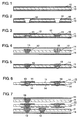
- Figs. 1 to 9 are sectional views showing steps of the method for manufacturing a multilayer printed wiring board according to a first embodiment of the present invention.
- Fig. 1 is a sectional view showing a step of pasting protective films 10 to electrically insulating substrate 11 according to the first embodiment.
- protective films 10 are laminated on both sides of electrically insulating substrate 11, which has a planar shape and made of insulating material (whose coefficient of thermal expansion is 40 to 70 ppm/°C).
- the insulating material is a composite of glass woven cloth and thermosetting resin such as epoxy-based resin.
- FIG. 2 is a sectional view showing a step of forming via holes. As shown in Fig. 2 , via holes 12, which penetrate through electrically insulating substrate 11 and protective films 10, are formed by laser drilling or the like.
- FIG. 3 is a sectional view showing a step of forming interlayer connection material 13 in via holes 12.
- interlayer connection material 13 (whose coefficient of thermal expansion is 16 to 35 ppm/°C) is formed in via holes 12.
- Interlayer connection material 13 is made of conductive paste having a coefficient of thermal expansion in the thickness direction lower than that of the insulating material forming electrically insulating substrate 11. The interlayer connection is made at a temperature of 180 to 400°C using interlayer connection material 13.
- Fig. 4 is a sectional view showing a step of laminating wiring members 14 .
- protective films 10 at both sides of electrically insulating substrate 11 shown in Fig.3 are removed.
- foil-like wiring members 14 containing, for example, copper is laminated on both sides of electrically insulating substrate 11.
- FIG. 5 is a sectional view showing a step of bonding wiring members 14 to electrically insulating substrate 11 and interlayer connection material 13.
- wiring members 14 are heated and pressurized at 180 to 200°C and at 3 to 5 MPa so as to be bonded to electrically insulating substrate 11 and interlayer connection material 13.
- interlayer connection material 13 is contracted in the thickness direction, and at the same time, wiring members 14 and interlayer connection material 13 are electrically connected to each other.
- Electrically insulating substrate 11 and interlayer connection material 13 that have wiring members 14 bonded thereto is cooled after the heating and pressurizing step. This causes a difference in the coefficient of thermal expansion between the different materials in the thickness direction. As a result, the internal stress allows interlayer connection material 13 to contract, thereby improving connection reliability in via holes 12.
- Fig. 6 is a sectional view showing a step of patterning wiring members 14. As shown in Fig.6 , wiring members 14 are patterned to complete double-sided wiring board 15. The patterning can be performed, for example, by etching.
- Fig. 7 is a sectional view showing a step of laminating wiring members 14 and electrically insulating substrates 11 which are filled with interlayer connection material 13. As shown in Fig. 7 , electrically insulating substrates 11, which are formed in the same steps as Figs. 1 to 4 and each filled with interlayer connection material 13 are laminated on both sides of double-sided wiring board 15. Then, two more wiring members 14 are laminated on both sides thereof.
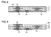
- FIG. 8 is a sectional view showing a step of heating and pressurizing wiring members 14. As shown in Fig.8 , wiring members 14 are heated and pressurized, which may be performed in the same manner as in the step shown in Fig.5 .
- the wiring boards thus laminated are cooled after the heating and pressurizing step. This causes a difference in the coefficient of thermal expansion between the different materials in the thickness direction. As a result, the internal stress allows interlayer connection material 13 to contract, thereby improving connection reliability in via holes 12.
- FIG. 9 is a sectional view showing a step of patterning wiring members 14. As shown in Fig.9 , wiring members 14 disposed on the outermost surfaces are patterned to complete multilayer printed wiring board 16 shown in Fig.9 .
- the patterning can be performed, for example, by etching.
- interlayer connection material 13 of multilayer printed wiring board 16 is larger in thickness than electrically insulating substrate 11 which is made of the insulating material and formed in the same wiring layer as interlayer connection material 13.
- the multilayer printed wiring board is a four-layer wiring board; however, the number of the wiring layers in the multilayer printed wiring board is not limited to four.
- the multilayer printed wiring board has at least two wiring layers and may have five or more wiring layers laminated by the similar steps.
- Multilayer printed wiring board 16 completed through the aforementioned steps is used at a temperature lower than the heating temperature used in the step of heating and pressurizing wiring members 14 shown in Fig. 5 .
- the temperature at which multilayer printed wiring board 16 is used is, for example, 60°C. This causes a difference in the coefficient of thermal expansion between the different materials in the thickness direction. As a result, the internal stress always functions to contract interlayer connecting material 13, thereby improving connection reliability in via holes 12.
- the insulating material is a composite of glass woven cloth and epoxy-based resin.
- it may be a composite of either glass unwoven cloth, aramid woven cloth, or aramid unwoven cloth and thermosetting resin such as epoxy resin.
- it may be a composite of either glass woven cloth, glass unwoven cloth, aramid woven cloth, or aramid unwoven cloth and thermoplastic resin whose glass transition temperature is 180°C or above.
- the insulating material may be made of a film material. Examples of the thermoplastic resin whose glass transition temperature is 180°C or above include wholly aromatic polyester resin, polyethersulfone, polyether ketone, and polyetheretherketone.
- Interlayer connection material 13 is formed by filling via holes 12 with the conductive paste.
- interlayer connection material 1.3 may be formed in via holes 12 by filled plating, conformal plating, evaporating, or sputtering.
- the interlayer connection material in the via holes has a coefficient of thermal expansion in the thickness direction lower than that of the insulating material in the thickness direction.
- the interlayer connection of the interlayer connection material is formed at a temperature higher than the operating temperature (for example, 60°C or less) of the multilayer printed wiring board. This causes a difference in the coefficient of thermal expansion between the different materials in the thickness direction of the printed wiring board in the environment in which it is used. As a result, the internal stress allows the interlayer connecting portion to contract, thereby achieving a multilayer printed wiring board having high connection reliability.
- the interlayer connection structure of the multilayer printed wiring board of the present invention provides high reliability of interlayer connection.
- Such multilayer printed wiring board is useful to the application relating to mounting substrates such as semiconductor packages and compact module components that are required to meet high reliability standards including minute wiring pattern and semiconductor packaging.
Landscapes
- Engineering & Computer Science (AREA)
- Manufacturing & Machinery (AREA)
- Microelectronics & Electronic Packaging (AREA)
- Production Of Multi-Layered Print Wiring Board (AREA)
Applications Claiming Priority (3)
| Application Number | Priority Date | Filing Date | Title |
|---|---|---|---|
| JP2006101750A JP2007280997A (ja) | 2006-04-03 | 2006-04-03 | 多層プリント配線基板の製造方法 |
| JP2006101749A JP2007280996A (ja) | 2006-04-03 | 2006-04-03 | 多層プリント配線基板 |
| PCT/JP2007/057394 WO2007116855A1 (ja) | 2006-04-03 | 2007-04-02 | 多層プリント配線基板及びその製造方法 |
Publications (2)
| Publication Number | Publication Date |
|---|---|
| EP1890524A1 true EP1890524A1 (de) | 2008-02-20 |
| EP1890524A4 EP1890524A4 (de) | 2009-07-01 |
Family
ID=38581145
Family Applications (1)
| Application Number | Title | Priority Date | Filing Date |
|---|---|---|---|
| EP07740830A Withdrawn EP1890524A4 (de) | 2006-04-03 | 2007-04-02 | Mehrschichtige bestückte leiterplatte und herstellungsverfahren dafür |
Country Status (3)
| Country | Link |
|---|---|
| US (2) | US7956293B2 (de) |
| EP (1) | EP1890524A4 (de) |
| WO (1) | WO2007116855A1 (de) |
Cited By (1)
| Publication number | Priority date | Publication date | Assignee | Title |
|---|---|---|---|---|
| EP2141973A1 (de) * | 2008-07-02 | 2010-01-06 | Nederlandse Organisatie voor toegepast-natuurwetenschappelijk Onderzoek TNO | Verfahren zur Bereitstellung leitfähiger Strukturen in einem mehrschichtigen Foliensystem und mehrschichtiges Foliensystem damit |
Families Citing this family (12)
| Publication number | Priority date | Publication date | Assignee | Title |
|---|---|---|---|---|
| JP5719560B2 (ja) * | 2009-10-21 | 2015-05-20 | 株式会社半導体エネルギー研究所 | 端子構造の作製方法 |
| US10083893B2 (en) | 2014-01-30 | 2018-09-25 | Toshiba Memory Corporation | Semiconductor device and semiconductor device manufacturing method |
| JP6696996B2 (ja) * | 2015-11-10 | 2020-05-20 | 株式会社村田製作所 | 樹脂多層基板およびその製造方法 |
| US12346290B2 (en) | 2022-07-13 | 2025-07-01 | Qumulo, Inc. | Workload allocation for file system maintenance |
| US11966592B1 (en) | 2022-11-29 | 2024-04-23 | Qumulo, Inc. | In-place erasure code transcoding for distributed file systems |
| US12292853B1 (en) | 2023-11-06 | 2025-05-06 | Qumulo, Inc. | Object-based storage with garbage collection and data consolidation |
| US11921677B1 (en) | 2023-11-07 | 2024-03-05 | Qumulo, Inc. | Sharing namespaces across file system clusters |
| US11934660B1 (en) | 2023-11-07 | 2024-03-19 | Qumulo, Inc. | Tiered data storage with ephemeral and persistent tiers |
| US12222903B1 (en) | 2024-08-09 | 2025-02-11 | Qumulo, Inc. | Global namespaces for distributed file systems |
| US12481625B1 (en) | 2024-11-12 | 2025-11-25 | Qumulo, Inc. | Integrating file system operations with network infrastructure |
| US12443568B1 (en) | 2024-11-12 | 2025-10-14 | Qumulo, Inc. | Verifying performance characteristics of network infrastructure for file systems |
| US12585563B1 (en) | 2025-12-01 | 2026-03-24 | Qumulo, Inc. | Caching for object stores |
Family Cites Families (12)
| Publication number | Priority date | Publication date | Assignee | Title |
|---|---|---|---|---|
| JPS59175796A (ja) | 1983-03-25 | 1984-10-04 | 日本電気株式会社 | 多層印刷配線板の製造方法 |
| DE69634597T2 (de) * | 1995-11-17 | 2006-02-09 | Kabushiki Kaisha Toshiba, Kawasaki | Mehrschichtige leiterplatte, vorgefertigtes material für diese leiterplatte, verfahren zur herstellung einer mehrschichtigen leiterplatte, packung elektronischer bauelemente und verfahren zur herstellung vertikaler, elektrisch leitender verbindungen |
| WO2001005204A1 (en) * | 1999-07-12 | 2001-01-18 | Ibiden Co., Ltd. | Method of manufacturing printed-circuit board |
| JP3923224B2 (ja) | 1999-09-20 | 2007-05-30 | 大日本印刷株式会社 | 多層プリント配線板及びその製造方法 |
| TW498707B (en) * | 1999-11-26 | 2002-08-11 | Matsushita Electric Industrial Co Ltd | Wiring substrate and production method thereof |
| JP2003023250A (ja) * | 2001-07-06 | 2003-01-24 | Denso Corp | 多層基板のおよびその製造方法 |
| JP2003198086A (ja) | 2001-12-25 | 2003-07-11 | Fujikura Ltd | 回路基板及び積層回路基板並びにそれらの製造方法 |
| WO2003071843A1 (en) * | 2002-02-22 | 2003-08-28 | Fujikura Ltd. | Multilayer wiring board, base for multilayer wiring board, printed wiring board, and its manufacturing method |
| DE10392162B4 (de) * | 2002-08-07 | 2012-02-23 | Denso Corporation | Schaltkreiskartenverbindungsstruktur und Herstellungsverfahren hierfür |
| TW200505304A (en) * | 2003-05-20 | 2005-02-01 | Matsushita Electric Industrial Co Ltd | Multilayer circuit board and method for manufacturing the same |
| JP4747707B2 (ja) * | 2004-11-09 | 2011-08-17 | ソニー株式会社 | 多層配線基板及び基板製造方法 |
| TWI295089B (en) * | 2004-12-28 | 2008-03-21 | Ngk Spark Plug Co | Wiring substrate and the manufacturing method of the same |
-
2007
- 2007-04-02 WO PCT/JP2007/057394 patent/WO2007116855A1/ja not_active Ceased
- 2007-04-02 US US11/910,560 patent/US7956293B2/en not_active Expired - Fee Related
- 2007-04-02 EP EP07740830A patent/EP1890524A4/de not_active Withdrawn
-
2010
- 2010-10-19 US US12/907,076 patent/US20110030207A1/en not_active Abandoned
Non-Patent Citations (2)
| Title |
|---|
| No further relevant documents disclosed * |
| See also references of WO2007116855A1 * |
Cited By (3)
| Publication number | Priority date | Publication date | Assignee | Title |
|---|---|---|---|---|
| EP2141973A1 (de) * | 2008-07-02 | 2010-01-06 | Nederlandse Organisatie voor toegepast-natuurwetenschappelijk Onderzoek TNO | Verfahren zur Bereitstellung leitfähiger Strukturen in einem mehrschichtigen Foliensystem und mehrschichtiges Foliensystem damit |
| WO2010002252A1 (en) * | 2008-07-02 | 2010-01-07 | Nederlandse Organisatie Voor Toegepast-Natuurwetenschappelijk Onderzoek Tno | Method of providing conductive structures in a multi-foil system and multifoil system comprising same |
| US10575411B2 (en) | 2008-07-02 | 2020-02-25 | Nederlandse Organisatie Voor Toegepast-Natuurwetenschappelijk Onderzoek Tno | Method of providing conductive structures in a multi-foil system and multifoil system comprising same |
Also Published As
| Publication number | Publication date |
|---|---|
| US20110030207A1 (en) | 2011-02-10 |
| EP1890524A4 (de) | 2009-07-01 |
| WO2007116855A1 (ja) | 2007-10-18 |
| US7956293B2 (en) | 2011-06-07 |
| US20090139761A1 (en) | 2009-06-04 |
Similar Documents
| Publication | Publication Date | Title |
|---|---|---|
| US7956293B2 (en) | Multilayer printed wiring board and manufacturing method thereof | |
| US8178191B2 (en) | Multilayer wiring board and method of making the same | |
| EP1811824B1 (de) | Mehrschichtige leiterplatte und herstellungsverfahren dafür | |
| KR102032171B1 (ko) | 전자 부품 내장 기판 및 그 제조 방법 | |
| US20050016764A1 (en) | Wiring substrate for intermediate connection and multi-layered wiring board and their production | |
| US8212365B2 (en) | Printed wiring board and manufacturing method thereof | |
| EP1814373A1 (de) | Mehrschichtige leiterplatte und herstellungsverfahren dafür | |
| US20080128911A1 (en) | Semiconductor package and method for manufacturing the same | |
| JP2011159855A (ja) | 局所多層回路基板、および局所多層回路基板の製造方法 | |
| JP2014502792A (ja) | 液晶高分子はんだマスクとアウタシール層とを有する電子デバイス及びその関連方法 | |
| WO2010129645A1 (en) | Method for integration of circuit components into the build-up layers of a printed wiring board | |
| US20160219710A1 (en) | Electronic component embedded printed circuit board and method of manufacturing the same | |
| JP2006253189A (ja) | 多層回路基板及びその製造方法 | |
| JP2007149870A (ja) | 回路基板及び回路基板の製造方法。 | |
| JP2011151048A (ja) | 電子部品の製造方法および電子部品 | |
| US20080308304A1 (en) | Multilayer Wiring Board and Its Manufacturing Method | |
| US7810232B2 (en) | Method of manufacturing a circuit board | |
| CN101361414A (zh) | 多层印刷线路基板及其制造方法 | |
| KR101886297B1 (ko) | 폴리이미드 코어를 이용한 박형 다층 인쇄회로기판 및 그 제조방법 | |
| KR100734244B1 (ko) | 다층 인쇄회로기판 및 그 제조방법 | |
| KR102884948B1 (ko) | 다층 기판의 제조 방법 | |
| JP4892924B2 (ja) | 多層プリント配線基板及びその製造方法 | |
| JP2007115952A (ja) | インターポーザ基板及びその製造方法 | |
| JP2004207266A (ja) | 接続基板の製造方法、および多層配線板の製造方法 | |
| US11317521B2 (en) | Resin flow restriction process and structure |
Legal Events
| Date | Code | Title | Description |
|---|---|---|---|
| PUAI | Public reference made under article 153(3) epc to a published international application that has entered the european phase |
Free format text: ORIGINAL CODE: 0009012 |
|
| 17P | Request for examination filed |
Effective date: 20070928 |
|
| AK | Designated contracting states |
Kind code of ref document: A1 Designated state(s): AT BE BG CH CY CZ DE DK EE ES FI FR GB GR HU IE IS IT LI LT LU LV MC MT NL PL PT RO SE SI SK TR |
|
| AX | Request for extension of the european patent |
Extension state: AL BA HR MK YU |
|
| RAX | Requested extension states of the european patent have changed |
Extension state: RS Extension state: MK Extension state: HR Extension state: BA Extension state: AL |
|
| RAP1 | Party data changed (applicant data changed or rights of an application transferred) |
Owner name: PANASONIC CORPORATION |
|
| DAX | Request for extension of the european patent (deleted) | ||
| RBV | Designated contracting states (corrected) |
Designated state(s): DE FR GB |
|
| A4 | Supplementary search report drawn up and despatched |
Effective date: 20090602 |
|
| STAA | Information on the status of an ep patent application or granted ep patent |
Free format text: STATUS: THE APPLICATION HAS BEEN WITHDRAWN |
|
| 18W | Application withdrawn |
Effective date: 20090622 |