EP1892584B1 - Agitateur et appareil de développement et appareil de formation d'images doté de celui-ci - Google Patents
Agitateur et appareil de développement et appareil de formation d'images doté de celui-ci Download PDFInfo
- Publication number
- EP1892584B1 EP1892584B1 EP07105095A EP07105095A EP1892584B1 EP 1892584 B1 EP1892584 B1 EP 1892584B1 EP 07105095 A EP07105095 A EP 07105095A EP 07105095 A EP07105095 A EP 07105095A EP 1892584 B1 EP1892584 B1 EP 1892584B1
- Authority
- EP
- European Patent Office
- Prior art keywords
- developer
- agitator
- developing
- wing
- image forming
- Prior art date
- Legal status (The legal status is an assumption and is not a legal conclusion. Google has not performed a legal analysis and makes no representation as to the accuracy of the status listed.)
- Ceased
Links
Images



Classifications
-
- G—PHYSICS
- G03—PHOTOGRAPHY; CINEMATOGRAPHY; ANALOGOUS TECHNIQUES USING WAVES OTHER THAN OPTICAL WAVES; ELECTROGRAPHY; HOLOGRAPHY
- G03G—ELECTROGRAPHY; ELECTROPHOTOGRAPHY; MAGNETOGRAPHY
- G03G15/00—Apparatus for electrographic processes using a charge pattern
- G03G15/06—Apparatus for electrographic processes using a charge pattern for developing
- G03G15/08—Apparatus for electrographic processes using a charge pattern for developing using a solid developer, e.g. powder developer
- G03G15/0822—Arrangements for preparing, mixing, supplying or dispensing developer
- G03G15/0887—Arrangements for conveying and conditioning developer in the developing unit, e.g. agitating, removing impurities or humidity
- G03G15/0889—Arrangements for conveying and conditioning developer in the developing unit, e.g. agitating, removing impurities or humidity for agitation or stirring
-
- G—PHYSICS
- G03—PHOTOGRAPHY; CINEMATOGRAPHY; ANALOGOUS TECHNIQUES USING WAVES OTHER THAN OPTICAL WAVES; ELECTROGRAPHY; HOLOGRAPHY
- G03G—ELECTROGRAPHY; ELECTROPHOTOGRAPHY; MAGNETOGRAPHY
- G03G15/00—Apparatus for electrographic processes using a charge pattern
- G03G15/06—Apparatus for electrographic processes using a charge pattern for developing
- G03G15/08—Apparatus for electrographic processes using a charge pattern for developing using a solid developer, e.g. powder developer
-
- G—PHYSICS
- G03—PHOTOGRAPHY; CINEMATOGRAPHY; ANALOGOUS TECHNIQUES USING WAVES OTHER THAN OPTICAL WAVES; ELECTROGRAPHY; HOLOGRAPHY
- G03G—ELECTROGRAPHY; ELECTROPHOTOGRAPHY; MAGNETOGRAPHY
- G03G15/00—Apparatus for electrographic processes using a charge pattern
- G03G15/06—Apparatus for electrographic processes using a charge pattern for developing
- G03G15/08—Apparatus for electrographic processes using a charge pattern for developing using a solid developer, e.g. powder developer
- G03G15/0822—Arrangements for preparing, mixing, supplying or dispensing developer
- G03G15/0877—Arrangements for metering and dispensing developer from a developer cartridge into the development unit
-
- G—PHYSICS
- G03—PHOTOGRAPHY; CINEMATOGRAPHY; ANALOGOUS TECHNIQUES USING WAVES OTHER THAN OPTICAL WAVES; ELECTROGRAPHY; HOLOGRAPHY
- G03G—ELECTROGRAPHY; ELECTROPHOTOGRAPHY; MAGNETOGRAPHY
- G03G21/00—Arrangements not provided for by groups G03G13/00 - G03G19/00, e.g. cleaning, elimination of residual charge
- G03G21/16—Mechanical means for facilitating the maintenance of the apparatus, e.g. modular arrangements
-
- G—PHYSICS
- G03—PHOTOGRAPHY; CINEMATOGRAPHY; ANALOGOUS TECHNIQUES USING WAVES OTHER THAN OPTICAL WAVES; ELECTROGRAPHY; HOLOGRAPHY
- G03G—ELECTROGRAPHY; ELECTROPHOTOGRAPHY; MAGNETOGRAPHY
- G03G2215/00—Apparatus for electrophotographic processes
- G03G2215/08—Details of powder developing device not concerning the development directly
- G03G2215/0802—Arrangements for agitating or circulating developer material
- G03G2215/0816—Agitator type
-
- G—PHYSICS
- G03—PHOTOGRAPHY; CINEMATOGRAPHY; ANALOGOUS TECHNIQUES USING WAVES OTHER THAN OPTICAL WAVES; ELECTROGRAPHY; HOLOGRAPHY
- G03G—ELECTROGRAPHY; ELECTROPHOTOGRAPHY; MAGNETOGRAPHY
- G03G2215/00—Apparatus for electrophotographic processes
- G03G2215/08—Details of powder developing device not concerning the development directly
- G03G2215/0802—Arrangements for agitating or circulating developer material
- G03G2215/085—Stirring member in developer container
Definitions
- the present invention relates an agitator for use in a developing apparatus of an image forming device, comprising a rotatable shaft and a wing extending from the rotatable shaft
- An image forming device such as a printer, that uses an electrophotography process, is an apparatus, which forms an electrostatic latent image on a photoconductor using a light exposing unit, develops the electrostatic latent image with a developer by using a developing apparatus to form a developer image, and then transfers and fixes the developer image onto a printing medium.
- the developer which is used for developing the electrostatic latent image in the developing apparatus, is either a one-component system developer or a two-component system developer.
- toner particles are electrified by friction with themselves or friction with a charging member. The electrified toner particles are moved onto a developing roller and then attached to an electrostatic latent image region of the photoconductor to form a developer image.
- a two-component system developer is a developer in which magnetic carrier particles are mixed with non-magnetic toner particles made of synthetic resins.
- the toner particles are electrified by friction with the carrier particles and with themselves.
- the electrified toner particles are moved onto the developing roller along with the carrier particles and then attached to an electrostatic latent image region of the photoconductor to form a developer image.
- a developing apparatus of an image forming device is provided with an agitator to electrify the toner particles of a developer by friction.
- a conventional agitator is shown in Figures 1A and 1B .
- the agitator 1 has a structure in which an agitating wing 3 is in the form of a helix on a rotary shaft 2.
- the agitator 1 rotates in a developer-containing space of a developer casing (not shown).
- toner particles and, if it is a two-component system, carrier particles are mixed with one another, and the toner particles are electrified by friction.
- the agitating wing 3 should be quickly rotated or the diameter thereof enlarged. To quickly rotate the agitating wing 3, a change to the design of the agitator driving system would be required, and to enlarge the diameter of the agitating wing 3 would require a layout change of the developing apparatus. Neither alternative is particularly desirable.
- agitator with an increased contact area of an agitating wing to thereby increase the electrification rate of a developer, without the requirement to quickly rotate the agitating wing or to increase the diameter of the agitating wing.
- aspects and embodiments of the present invention provide a developing apparatus and an image forming device having one or more agitators with the characteristics described above.
- JP2005148288 D2
- JP2005148288 D2
- a developer agitator 40 of the present invention includes a rotatable shaft 41, an agitating wing 42 disposed in the form of a helix on the circumferential surface of the shaft 41, and an uneven part 43 formed on a surface of the agitating wing 42.
- the agitator 40 constructed as described above can be used for electrifying a developer by friction in, for example, a developing apparatus 100 as illustrated in Figure 4 .
- the uneven part 43 formed on the surface of the agitating wing 42 increases the contact area for the developer, and thus improves the electrification rate of the developer.
- the conventional agitating wing 3 (see Figures 1A and 1B ) has a smooth surface, but the agitating wing 42 of the developer agitator 40 according to the embodiment of the present invention has the uneven part 43 formed on the surface thereof, thereby allowing a surface area of the agitating wing 42 to be enlarged compared with the conventional agitating wing 3. Accordingly, the contact area of the agitating wing 42 and the developer is increased, and thus without the requirement to quickly rotate the agitating wing 42 or increase the diameter thereof, the contact time between toner particles and, in a two component system developer, carrier particles of the developer, is lengthened and the number of particles contacted thereby is increased, increasing the electrification rate of the developer.
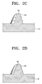
- the uneven part 43 as described above can have a waved structure or a stepped structure, as illustrated by 53 and 63 in Figures 2C and 2D , respectively.
- the uneven part 43 can be configured in any combination of both waved and stepped structures that is capable of increasing the surface area thereof, an embodiment being the uneven part 43 shown in Figure 2B .
- the uneven part 43 has the same structure and cross-section along the entire length of the agitator 40.
- the uneven part 43 can vary along the length of the agitator 40.
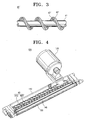
- FIG 3 is a perspective view exemplifying a section of a developer agitator 40' according to another embodiment of the present invention.
- the developer agitator 40' has the same basic structure as that of the developer agitator 40 of the embodiment as described above and shown in Figure 2A , which includes a rotatable shaft 41, an agitating wing 42 disposed in the form of a helix on a circumferential surface of the shaft 41, and an uneven part 43 formed on a surface of the agitating wing 42.
- the orientation of the uneven part 43' is different from that of the uneven part 43 shown in Figure 2A .
- the uneven part 43' is oriented in the longitudinal direction of the agitating wing 42', whereas in the previous embodiment shown in Figure 2A , the uneven part 43 is oriented in the transverse direction of the agitating wing 42.
- the surface area of the agitating wing 42' is also enlarged, so that the developer agitator 40' can obtain the same results as that of the agitator 40 in the previous embodiment shown in Figure 2A .
- the formed orientation of the uneven part 43 is not limited to the examples illustrated in the drawings.
- the uneven part 43 can be formed in any other structure, for example, a slightly slanted structure that is capable increasing the surface area of the agitating wing 42.
- FIG 4 is a perspective view schematically exemplifying a developing apparatus 100 to which the developer agitator 40, according to the embodiment of the present invention as described above and shown in Figure 2A , is applied.
- the developing apparatus 100 includes a developing casing 110 having a developer-containing space formed in a predetermined shape.
- the developing casing 110 is provided with a developer inlet and a developer outlet.
- a developer cartridge 120 is connected to the developer inlet, and a developing roller 130 and a developer supplying roller 140 are rotatably disposed at the developer outlet.
- the developer agitator 40 includes a first developer agitator 410 and a second developer agitator 420, which are rotatably disposed in the developer-containing space of the developing casing 110.
- a developer contained in the developer-containing space is agitated by the first and second developer agitators 410 and 420, so that the developer is electrified by friction.
- the agitating wings 42 of the developer agitators 410 and 420 have the contact areas for the developer enlarged by the uneven parts 43 formed on the surfaces thereof, the electrification rate of the developer is higher than if an agitator 1 with a smooth agitating wing 2 as shown in Figure 1A was used.
- Figure 5 is a graph exemplifying the toner-electrification amount is compared to agitating time using the developer agitator according to an embodiment of the present invention.
- the toner-electrification amount was saturated in a shorter time compared to using a conventional developer agitator.
- the toner-electrification amount should be at least 70% of a saturated state.
- a reference E indicates a suitable development image point.
- the toner-electrification amount has reached the required value before the suitable development image point E, so that the developer agitator of the embodiment of the present invention can be used in high speed printing with a shorter development image point E.
- FIG. 6 is a cross sectional view showing a section of an example image forming device to which the developing apparatus 100 of Figure 4 as described above is applied.
- a photoconductor 200 is disposed to face the developing roller 130 of the developing apparatus 100.
- a charging roller 210 is rotatably disposed in contact with the photoconductor 200 to charge the photoconductor 200.
- a scanning unit 220 using a light source such as a laser or light emitting diode (LED), scans a beam onto a surface of the photoconductor 200 electrified by the charging roller 210, and thus forms a predetermined electrostatic latent image on the surface of the photoconductor 200.
- a light source such as a laser or light emitting diode (LED)
- the electrostatic latent image of the photoconductor 200 is developed into a developer image by the developing apparatus 100, and the developer image is transferred onto a printing medium P, such as paper, transparency, etc., which is conveyed between a transferring roller 230 and the photoconductor 200.
- the developer image transferred onto the printing medium P is fixed on the printing medium P when it passes through a fusing apparatus 240.
- the image forming process as described above is the same as that of the conventional image forming device, except that by using the agitator 40 contained in the developer 100, the electrification rate of the developer is increased by the developer agitator 40 as described above, thereby allowing the image forming device to be adapted to use in high speed printing.
- the developer agitator, and the developing apparatus and the image forming device having the same can not only smoothly agitate the developer, but also increase the electrification rate of the developer. Accordingly, the developer agitator 40, and the developing apparatus 100 and the image forming device having the same according to the embodiments of the present invention can obtain an electrification rate of the developer required for high speed printing, thereby allowing the image forming device to be operated at a high speed.
Landscapes
- Physics & Mathematics (AREA)
- General Physics & Mathematics (AREA)
- Dry Development In Electrophotography (AREA)
Claims (8)
- Agitateur prévu pour être utilisé dans un appareil de développement d'un dispositif de formation d'image, comprenant un arbre rotatif et une aile hélicoïdale qui dépasse autour de l'arbre rotatif, caractérisé en ce qu'au moins une partie de l'aile a une surface irrégulière pour augmenter la superficie de l'aile afin d'augmenter une surface de contact avec une substance à agiter.
- Agitateur selon la revendication 1, dans lequel la surface irrégulière est en forme de structure en gradins, ou de structure ondulée, ou d'une combinaison des deux.
- Agitateur selon la revendication 2, dans lequel les structures ondulée et/ou en gradins varient sur la longueur de l'arbre.
- Agitateur selon la revendication 1 ou la revendication 2, dans lequel la partie irrégulière est orientée dans la direction longitudinale de l'aile d'agitation.
- Agitateur selon la revendication 1 ou la revendication 2, dans lequel la partie irrégulière est orientée dans la direction transversale de l'aile d'agitation.
- Agitateur selon l'une quelconque des revendications précédentes, dans lequel la substance à agiter comprend un agent de développement.
- Appareil de développement comprenant : un agent de développement, un boîtier de développement comportant un espace contenant l'agent de développement pour renfermer l'agent de développement, un rouleau de développement pour tourner dans le boîtier de développement, un rouleau fournisseur d'agent de développement pour tourner dans le boîtier de développement en faisant face au rouleau de développement, grâce à quoi l'agent de développement de l'espace contenant l'agent de développement est fourni au rouleau de développement et à un agitateur selon l'une quelconque des revendications précédentes pour électrifier par friction un agent de développement contenu dans l'espace contenant l'agent de développement.
- Dispositif de formation d'image comprenant un photoconducteur sur lequel est formée une image latente électrostatique, un appareil de transfert pour transférer sur un support d'impression l'image de l'agent de développement formée sur le photoconducteur, un appareil de fusion pour fixer l'image de l'agent de développement sur un support d'impression et un appareil de développement selon la revendication 7.
Applications Claiming Priority (1)
| Application Number | Priority Date | Filing Date | Title |
|---|---|---|---|
| KR1020060081259A KR20080018704A (ko) | 2006-08-25 | 2006-08-25 | 교반장치, 이 교반장치를 구비하는 현상장치 및화상형성장치 |
Publications (2)
| Publication Number | Publication Date |
|---|---|
| EP1892584A1 EP1892584A1 (fr) | 2008-02-27 |
| EP1892584B1 true EP1892584B1 (fr) | 2009-07-29 |
Family
ID=38859066
Family Applications (1)
| Application Number | Title | Priority Date | Filing Date |
|---|---|---|---|
| EP07105095A Ceased EP1892584B1 (fr) | 2006-08-25 | 2007-03-28 | Agitateur et appareil de développement et appareil de formation d'images doté de celui-ci |
Country Status (5)
| Country | Link |
|---|---|
| US (1) | US7711290B2 (fr) |
| EP (1) | EP1892584B1 (fr) |
| KR (1) | KR20080018704A (fr) |
| CN (1) | CN101131556A (fr) |
| DE (1) | DE602007001743D1 (fr) |
Families Citing this family (7)
| Publication number | Priority date | Publication date | Assignee | Title |
|---|---|---|---|---|
| JP5070303B2 (ja) * | 2010-01-25 | 2012-11-14 | シャープ株式会社 | 現像装置及びこれを用いる画像形成装置 |
| KR101692417B1 (ko) * | 2011-12-29 | 2017-01-05 | 인텔 코포레이션 | 다이렉트 액세스를 갖는 다중-레벨 메모리 |
| JP6213336B2 (ja) * | 2014-03-26 | 2017-10-18 | ブラザー工業株式会社 | 画像形成装置 |
| KR20160008429A (ko) | 2014-07-14 | 2016-01-22 | 삼성전자주식회사 | 현상장치 및 이를 구비한 화상형성장치 |
| WO2019190136A1 (fr) * | 2018-03-27 | 2019-10-03 | 계명대학교 산학협력단 | Embout de mélange de matériau d'empreinte dentaire |
| KR102018458B1 (ko) * | 2018-03-27 | 2019-09-04 | 계명대학교 산학협력단 | 치과용 인상재 믹싱 팁 |
| KR102016849B1 (ko) * | 2018-03-27 | 2019-08-30 | 계명대학교 산학협력단 | 치과용 인상재 믹싱 팁 |
Family Cites Families (16)
| Publication number | Priority date | Publication date | Assignee | Title |
|---|---|---|---|---|
| SU594314A1 (ru) * | 1975-03-24 | 1978-02-25 | Кузбасский Политехнический Институт | Шнекова бурова штанга |
| US4146323A (en) * | 1977-06-29 | 1979-03-27 | Xerox Corporation | Auger for a development system |
| US4878088A (en) * | 1985-07-02 | 1989-10-31 | Fujitsu Limited | Developing unit of electrophotographic apparatus |
| JPH04274468A (ja) | 1991-03-01 | 1992-09-30 | Brother Ind Ltd | 現像装置 |
| US5519470A (en) * | 1994-03-04 | 1996-05-21 | Xerox Corporation | Cross mixing paddle wheel |
| US5758238A (en) * | 1996-11-25 | 1998-05-26 | Xerox Corporation | Auger configuration for eliminating auger mark print defect |
| US6281961B1 (en) * | 1998-01-14 | 2001-08-28 | Minolta Co., Ltd. | Developing device with mechanism for smoothly circulating developer |
| JP4274468B2 (ja) | 2002-03-13 | 2009-06-10 | ツァワー ゲィリー | 歯のホワイトニング用具及び歯のホワイトニング方法 |
| JP4208645B2 (ja) | 2003-06-03 | 2009-01-14 | キヤノン株式会社 | 現像剤補給容器 |
| JP4225135B2 (ja) * | 2003-06-26 | 2009-02-18 | コニカミノルタビジネステクノロジーズ株式会社 | 現像装置および画像形成装置 |
| JP2005148288A (ja) | 2003-11-13 | 2005-06-09 | Sharp Corp | 現像剤攪拌部材、現像装置、および画像形成装置 |
| US7757522B2 (en) * | 2004-06-29 | 2010-07-20 | Whirlpool Corporation | Washing machine agitator assembly |
| JP2006227598A (ja) | 2005-01-18 | 2006-08-31 | Canon Inc | 現像剤搬送スクリュー |
| JP2006227149A (ja) * | 2005-02-16 | 2006-08-31 | Matsushita Electric Ind Co Ltd | 現像装置及びプロセスカートリッジ並びに画像形成装置 |
| JP4622774B2 (ja) * | 2005-09-21 | 2011-02-02 | ブラザー工業株式会社 | 画像形成装置、現像装置、及びトナーカートリッジ |
| JP4786284B2 (ja) * | 2005-10-07 | 2011-10-05 | 株式会社リコー | 現像装置、プロセスユニット及び画像形成装置 |
-
2006
- 2006-08-25 KR KR1020060081259A patent/KR20080018704A/ko not_active Withdrawn
-
2007
- 2007-02-20 US US11/708,005 patent/US7711290B2/en not_active Expired - Fee Related
- 2007-03-20 CN CNA2007100882596A patent/CN101131556A/zh active Pending
- 2007-03-28 DE DE602007001743T patent/DE602007001743D1/de active Active
- 2007-03-28 EP EP07105095A patent/EP1892584B1/fr not_active Ceased
Also Published As
| Publication number | Publication date |
|---|---|
| US7711290B2 (en) | 2010-05-04 |
| KR20080018704A (ko) | 2008-02-28 |
| CN101131556A (zh) | 2008-02-27 |
| EP1892584A1 (fr) | 2008-02-27 |
| DE602007001743D1 (de) | 2009-09-10 |
| US20080050152A1 (en) | 2008-02-28 |
Similar Documents
| Publication | Publication Date | Title |
|---|---|---|
| US7881640B2 (en) | Member for agitating and conveying developer, developing device, and image forming apparatus having the same | |
| EP1892584B1 (fr) | Agitateur et appareil de développement et appareil de formation d'images doté de celui-ci | |
| JP4646728B2 (ja) | 現像装置及びこれを備えた画像形成装置 | |
| JP5660312B2 (ja) | 現像剤搬送装置、現像剤収容器、現像装置、プロセスユニット及び画像形成装置 | |
| JP6079242B2 (ja) | 現像剤撹拌搬送部材、現像装置、及び画像形成装置 | |
| CN104808463B (zh) | 显影设备,处理盒及电子照相成像装置 | |
| JP3903666B2 (ja) | 現像装置および画像形成装置 | |
| US20080145106A1 (en) | Image developing unit and image forming apparatus having the same | |
| US10146157B2 (en) | Development apparatus having a multiple screw portion conveyance screw | |
| US10409198B2 (en) | Feeding screw and developing device | |
| US8121523B2 (en) | Developer station with tapered auger system | |
| JP2006276860A (ja) | 現像素材用特殊排出ポートを有する電子写真現像器ユニット | |
| JP5887319B2 (ja) | 現像装置およびそれを備えた画像形成装置 | |
| JP7416274B2 (ja) | 現像装置およびそれを備えた画像形成装置 | |
| US10126683B2 (en) | Developing apparatus | |
| JP6662430B2 (ja) | 撹拌搬送部材、現像装置、及び画像形成装置 | |
| CN107870544B (zh) | 显影装置以及具备该显影装置的图像形成装置 | |
| CN110133975B (zh) | 显影装置 | |
| EP1995643A2 (fr) | Appareil de formation d'image, appareil de développement et rouleau de développement, contenant une portion magnétique, pour l'appareil de formation d'image | |
| JP7379838B2 (ja) | 現像装置および画像形成装置 | |
| JP2009020354A (ja) | 現像装置、画像形成方法、画像形成装置およびプロセスカートリッジ | |
| JP6828399B2 (ja) | 現像剤搬送部材、現像装置および画像形成装置 | |
| JP2017062520A (ja) | 現像剤撹拌搬送部材、現像装置、及び画像形成装置 | |
| JP6950225B2 (ja) | 現像装置、組立体及び画像形成装置 | |
| JP5594906B2 (ja) | 撹拌部材及びそれを備えた現像装置並びに画像形成装置 |
Legal Events
| Date | Code | Title | Description |
|---|---|---|---|
| PUAI | Public reference made under article 153(3) epc to a published international application that has entered the european phase |
Free format text: ORIGINAL CODE: 0009012 |
|
| AK | Designated contracting states |
Kind code of ref document: A1 Designated state(s): AT BE BG CH CY CZ DE DK EE ES FI FR GB GR HU IE IS IT LI LT LU LV MC MT NL PL PT RO SE SI SK TR |
|
| AX | Request for extension of the european patent |
Extension state: AL BA HR MK YU |
|
| 17P | Request for examination filed |
Effective date: 20080806 |
|
| AKX | Designation fees paid |
Designated state(s): DE FR GB NL |
|
| GRAP | Despatch of communication of intention to grant a patent |
Free format text: ORIGINAL CODE: EPIDOSNIGR1 |
|
| RAP1 | Party data changed (applicant data changed or rights of an application transferred) |
Owner name: SAMSUNG ELECTRONICS CO., LTD. |
|
| GRAS | Grant fee paid |
Free format text: ORIGINAL CODE: EPIDOSNIGR3 |
|
| GRAA | (expected) grant |
Free format text: ORIGINAL CODE: 0009210 |
|
| AK | Designated contracting states |
Kind code of ref document: B1 Designated state(s): DE FR GB NL |
|
| REG | Reference to a national code |
Ref country code: GB Ref legal event code: FG4D |
|
| REF | Corresponds to: |
Ref document number: 602007001743 Country of ref document: DE Date of ref document: 20090910 Kind code of ref document: P |
|
| PLBE | No opposition filed within time limit |
Free format text: ORIGINAL CODE: 0009261 |
|
| STAA | Information on the status of an ep patent application or granted ep patent |
Free format text: STATUS: NO OPPOSITION FILED WITHIN TIME LIMIT |
|
| 26N | No opposition filed |
Effective date: 20100503 |
|
| REG | Reference to a national code |
Ref country code: FR Ref legal event code: PLFP Year of fee payment: 10 |
|
| REG | Reference to a national code |
Ref country code: FR Ref legal event code: PLFP Year of fee payment: 11 |
|
| REG | Reference to a national code |
Ref country code: NL Ref legal event code: PD Owner name: S-PRINTING SOLUTION CO., LTD.; KO Free format text: DETAILS ASSIGNMENT: CHANGE OF OWNER(S), ASSIGNMENT; FORMER OWNER NAME: SAMSUNG ELECTRONICS CO., LTD. Effective date: 20170221 |
|
| REG | Reference to a national code |
Ref country code: GB Ref legal event code: 732E Free format text: REGISTERED BETWEEN 20170406 AND 20170412 |
|
| REG | Reference to a national code |
Ref country code: DE Ref legal event code: R082 Ref document number: 602007001743 Country of ref document: DE Representative=s name: HOEFER & PARTNER PATENTANWAELTE MBB, DE Ref country code: DE Ref legal event code: R081 Ref document number: 602007001743 Country of ref document: DE Owner name: HP PRINTING KOREA CO., LTD., SUWON-SI, KR Free format text: FORMER OWNER: SAMSUNG ELECTRONICS CO., LTD., SUWON-SI, GYEONGGI-DO, KR Ref country code: DE Ref legal event code: R081 Ref document number: 602007001743 Country of ref document: DE Owner name: HEWLETT-PACKARD DEVELOPMENT COMPANY, L.P., SPR, US Free format text: FORMER OWNER: SAMSUNG ELECTRONICS CO., LTD., SUWON-SI, GYEONGGI-DO, KR Ref country code: DE Ref legal event code: R081 Ref document number: 602007001743 Country of ref document: DE Owner name: S-PRINTING SOLUTION CO., LTD., SUWON-SI, KR Free format text: FORMER OWNER: SAMSUNG ELECTRONICS CO., LTD., SUWON-SI, GYEONGGI-DO, KR |
|
| REG | Reference to a national code |
Ref country code: FR Ref legal event code: TP Owner name: S-PRINTING SOLUTION CO., LTD., KR Effective date: 20170912 |
|
| REG | Reference to a national code |
Ref country code: FR Ref legal event code: PLFP Year of fee payment: 12 |
|
| REG | Reference to a national code |
Ref country code: NL Ref legal event code: HC Owner name: HP PRINTING KOREA CO., LTD.; KR Free format text: DETAILS ASSIGNMENT: CHANGE OF OWNER(S), CHANGE OF OWNER(S) NAME; FORMER OWNER NAME: S-PRINTING SOLUTION CO., LTD. Effective date: 20180816 |
|
| REG | Reference to a national code |
Ref country code: DE Ref legal event code: R082 Ref document number: 602007001743 Country of ref document: DE Ref country code: DE Ref legal event code: R081 Ref document number: 602007001743 Country of ref document: DE Owner name: HP PRINTING KOREA CO., LTD., SUWON-SI, KR Free format text: FORMER OWNER: S-PRINTING SOLUTION CO., LTD., SUWON-SI, GYEONGGI-DO, KR Ref country code: DE Ref legal event code: R081 Ref document number: 602007001743 Country of ref document: DE Owner name: HEWLETT-PACKARD DEVELOPMENT COMPANY, L.P., SPR, US Free format text: FORMER OWNER: S-PRINTING SOLUTION CO., LTD., SUWON-SI, GYEONGGI-DO, KR |
|
| PGFP | Annual fee paid to national office [announced via postgrant information from national office to epo] |
Ref country code: NL Payment date: 20190225 Year of fee payment: 13 |
|
| PGFP | Annual fee paid to national office [announced via postgrant information from national office to epo] |
Ref country code: DE Payment date: 20190219 Year of fee payment: 13 Ref country code: GB Payment date: 20190222 Year of fee payment: 13 |
|
| PGFP | Annual fee paid to national office [announced via postgrant information from national office to epo] |
Ref country code: DE Payment date: 20190219 Year of fee payment: 13 Ref country code: FR Payment date: 20190220 Year of fee payment: 13 |
|
| REG | Reference to a national code |
Ref country code: NL Ref legal event code: PD Owner name: HEWLETT-PACKARD DEVELOPMENT COMPANY, L.P.; US Free format text: DETAILS ASSIGNMENT: CHANGE OF OWNER(S), CHANGE OF LEGAL ENTITY; FORMER OWNER NAME: SAMSUNG ELECTRONICS CO., LTD. Effective date: 20191030 |
|
| REG | Reference to a national code |
Ref country code: DE Ref legal event code: R081 Ref document number: 602007001743 Country of ref document: DE Owner name: HEWLETT-PACKARD DEVELOPMENT COMPANY, L.P., SPR, US Free format text: FORMER OWNER: HP PRINTING KOREA CO., LTD., SUWON-SI, GYEONGGI-DO, KR |
|
| REG | Reference to a national code |
Ref country code: GB Ref legal event code: 732E Free format text: REGISTERED BETWEEN 20191212 AND 20191218 |
|
| REG | Reference to a national code |
Ref country code: DE Ref legal event code: R119 Ref document number: 602007001743 Country of ref document: DE |
|
| REG | Reference to a national code |
Ref country code: NL Ref legal event code: MM Effective date: 20200401 |
|
| PG25 | Lapsed in a contracting state [announced via postgrant information from national office to epo] |
Ref country code: NL Free format text: LAPSE BECAUSE OF NON-PAYMENT OF DUE FEES Effective date: 20200401 |
|
| PG25 | Lapsed in a contracting state [announced via postgrant information from national office to epo] |
Ref country code: DE Free format text: LAPSE BECAUSE OF NON-PAYMENT OF DUE FEES Effective date: 20201001 Ref country code: FR Free format text: LAPSE BECAUSE OF NON-PAYMENT OF DUE FEES Effective date: 20200331 |
|
| GBPC | Gb: european patent ceased through non-payment of renewal fee |
Effective date: 20200328 |
|
| PG25 | Lapsed in a contracting state [announced via postgrant information from national office to epo] |
Ref country code: GB Free format text: LAPSE BECAUSE OF NON-PAYMENT OF DUE FEES Effective date: 20200328 |