EP1892733A2 - Verfahren, Element und Vorrichtung zur Regulierung des Widerstands - Google Patents
Verfahren, Element und Vorrichtung zur Regulierung des Widerstands Download PDFInfo
- Publication number
- EP1892733A2 EP1892733A2 EP07015619A EP07015619A EP1892733A2 EP 1892733 A2 EP1892733 A2 EP 1892733A2 EP 07015619 A EP07015619 A EP 07015619A EP 07015619 A EP07015619 A EP 07015619A EP 1892733 A2 EP1892733 A2 EP 1892733A2
- Authority
- EP
- European Patent Office
- Prior art keywords
- cut
- resistance
- resistance film
- cutting
- film
- Prior art date
- Legal status (The legal status is an assumption and is not a legal conclusion. Google has not performed a legal analysis and makes no representation as to the accuracy of the status listed.)
- Withdrawn
Links
Images


Classifications
-
- H—ELECTRICITY
- H05—ELECTRIC TECHNIQUES NOT OTHERWISE PROVIDED FOR
- H05K—PRINTED CIRCUITS; CASINGS OR CONSTRUCTIONAL DETAILS OF ELECTRIC APPARATUS; MANUFACTURE OF ASSEMBLAGES OF ELECTRICAL COMPONENTS
- H05K1/00—Printed circuits
- H05K1/16—Printed circuits incorporating printed electric components, e.g. printed resistors, capacitors or inductors
- H05K1/167—Printed circuits incorporating printed electric components, e.g. printed resistors, capacitors or inductors incorporating printed resistors
-
- H—ELECTRICITY
- H01—ELECTRIC ELEMENTS
- H01C—RESISTORS
- H01C17/00—Apparatus or processes specially adapted for manufacturing resistors
- H01C17/22—Apparatus or processes specially adapted for manufacturing resistors adapted for trimming
- H01C17/24—Apparatus or processes specially adapted for manufacturing resistors adapted for trimming by removing or adding resistive material
- H01C17/242—Apparatus or processes specially adapted for manufacturing resistors adapted for trimming by removing or adding resistive material by laser
-
- H—ELECTRICITY
- H05—ELECTRIC TECHNIQUES NOT OTHERWISE PROVIDED FOR
- H05K—PRINTED CIRCUITS; CASINGS OR CONSTRUCTIONAL DETAILS OF ELECTRIC APPARATUS; MANUFACTURE OF ASSEMBLAGES OF ELECTRICAL COMPONENTS
- H05K2203/00—Indexing scheme relating to apparatus or processes for manufacturing printed circuits covered by H05K3/00
- H05K2203/10—Using electric, magnetic and electromagnetic fields; Using laser light
- H05K2203/107—Using laser light
-
- H—ELECTRICITY
- H05—ELECTRIC TECHNIQUES NOT OTHERWISE PROVIDED FOR
- H05K—PRINTED CIRCUITS; CASINGS OR CONSTRUCTIONAL DETAILS OF ELECTRIC APPARATUS; MANUFACTURE OF ASSEMBLAGES OF ELECTRICAL COMPONENTS
- H05K2203/00—Indexing scheme relating to apparatus or processes for manufacturing printed circuits covered by H05K3/00
- H05K2203/14—Related to the order of processing steps
- H05K2203/1476—Same or similar kind of process performed in phases, e.g. coarse patterning followed by fine patterning
-
- H—ELECTRICITY
- H05—ELECTRIC TECHNIQUES NOT OTHERWISE PROVIDED FOR
- H05K—PRINTED CIRCUITS; CASINGS OR CONSTRUCTIONAL DETAILS OF ELECTRIC APPARATUS; MANUFACTURE OF ASSEMBLAGES OF ELECTRICAL COMPONENTS
- H05K2203/00—Indexing scheme relating to apparatus or processes for manufacturing printed circuits covered by H05K3/00
- H05K2203/17—Post-manufacturing processes
- H05K2203/171—Tuning, e.g. by trimming of printed components or high frequency circuits
-
- H—ELECTRICITY
- H05—ELECTRIC TECHNIQUES NOT OTHERWISE PROVIDED FOR
- H05K—PRINTED CIRCUITS; CASINGS OR CONSTRUCTIONAL DETAILS OF ELECTRIC APPARATUS; MANUFACTURE OF ASSEMBLAGES OF ELECTRICAL COMPONENTS
- H05K2203/00—Indexing scheme relating to apparatus or processes for manufacturing printed circuits covered by H05K3/00
- H05K2203/17—Post-manufacturing processes
- H05K2203/175—Configurations of connections suitable for easy deletion, e.g. modifiable circuits or temporary conductors for electroplating; Processes for deleting connections
-
- Y—GENERAL TAGGING OF NEW TECHNOLOGICAL DEVELOPMENTS; GENERAL TAGGING OF CROSS-SECTIONAL TECHNOLOGIES SPANNING OVER SEVERAL SECTIONS OF THE IPC; TECHNICAL SUBJECTS COVERED BY FORMER USPC CROSS-REFERENCE ART COLLECTIONS [XRACs] AND DIGESTS
- Y10—TECHNICAL SUBJECTS COVERED BY FORMER USPC
- Y10T—TECHNICAL SUBJECTS COVERED BY FORMER US CLASSIFICATION
- Y10T29/00—Metal working
- Y10T29/49—Method of mechanical manufacture
- Y10T29/49002—Electrical device making
- Y10T29/49082—Resistor making
Definitions
- the present invention relates to a resistance adjusting method, a resistance adjusting element and a resistance adjusting device.
- a chip-like resistors has been used as a circuit element formed on an electronic circuit board. It is necessary to adjust a value of resistance of each chip-like resistor in order to adjust output characteristics of the electronic circuit board as a whole after mounting the resistor on the electronic circuit board.
- Such a chip-like resistor which is so called as a resistor film has been obtained by cutting off a part of calcined resistance such as a carbon paste with the use of a laser beam or the like so as to have a desired resistance value.
- an object of the present invention is to provide a resistance adjusting method, a resistance adjusting element and a resistance adjusting device which are capable of simply recognizing a terminal end of a cut-off part in such a case that a plurality of cut-off parts are formed in a resistance film and resistances thereof are adjusted.
- a resistance adjusting method characterized by comprising a first cut-off step for obtaining a first cut-off part in a resistance film, a second cut-off step, subsequent to the first cut-off step, for obtaining a second cut-off part by cutting off the resistance film in a direction different from a direction in which the first cut-off step is carried out, so that the second cut-off part is continuous to the first cut-off part substantially at a position of one end of the first cut-off part so that the second cut-off part serves as a marker, and a third cut-off step for obtaining a third cut-off part by recognizing the position of the second cut-off part and cutting off the resistance film in a direction different from the direction in which the second cut-off part is carried out, so as to leave a part having a length capable of preventing cracking of the resistance film remained.
- a resistance adjusting element characterized by comprising a first cut-off part which extends from one widthwise end toward the other widthwise end of a resistance film, a second cut-off part which extends in a direction different from a direction of the first cut-off part so as to cross the first cut-off part substantially at a position of an end of the first cut-off part, and a third cut-off part which extends between the second cut-off part and the other widthwise end of the resistance film.
- a resistance adjusting device characterized by comprising a carrier portion on which a product provided with a resistance film is set; a laser irradiating portion for irradiating a laser beam onto the resistance film so as to form a cut-off part in a resistance film; a drive portion capable of causing a laser irradiating portion to scan in a plurality of axial directions; an image recognizing portion for recognizing a second cut-off part during preliminary resistance adjustment for both first cut-off part formed in the resistance film and the second cut-off part formed so as to cross the first cut-off part substantially at a position of an end part of the first cut-off part, and for inputting a position of the second cut-off part to a control portion; and a final resistance adjustment control portion for causing the drive portion to scan so as to form a third cut-off part in the resistance film, being based upon the position of the second cut-off part recognized by the image recognizing portion.
- a terminal end of a cut-off part can be simply recognized when a plurality of cut-off parts are to be formed in a resistance film so as to adjust resistances.
- Fig. 1 is a top view illustrating an electronic circuit board for processing a signal from an air-flow sensor used in an engine of an automobile
- Fig. 2 is a side sectional view illustrating a resistance adjusting element part in Fig. 1.
- the electronic circuit board 1 shown in Fig. 1 is adapted to be used in a signal process for amplifying a signal from an air-flow sensor and so forth, having, in particular, a relatively small size, that is, each side thereof has about 2 cm.
- the electronic circuit board is composed of a substrate 2 made of insulating material such as ceramic, various elements such as an operation amplifier and the like mounted on the substrate 2, conductors printed on the substrate 2, for connecting these elements to one another, and resistance film elements 3a to 3f serving as resistance adjustment elements, printed on the substrate, similar to the conductors, and spanning between the conductors.
- a lower layer conductor 4a serving as a first layer is printed, direct on the substrate 2 of the electronic circuit board 1, and then, an insulating layer 5 is formed on the lower layer conductor 4a.
- an upper layer conductor 4b serving as a second layer is printed on the insulating layer 5, and is then covered thereover with an overcoat glass layer 6.
- the resistance film 3 is printed, spanning between different upper layer conductors 4b after the upper layer conductors 4b are printed on the insulating layer 5, and the overcoat glass layer 6 is then formed so as to cover both resistance film 3 and upper layer conductors 4b.
- the resistance film 3 is formed so as to have a dried film thickness of 12 ⁇ m, that is, it is formed in such a way that a carbon paste is printed on the insulating layer 5 and the upper layer conductors 4b, is then calcined at a temperature of 860 degree C.
- the resistance film 3 is adapted to be cut-off in part by a laser beam in order to adjust a resistance value, as will be described later. However, should the power of the laser beam be excessive, not only the resistance film but also the insulating layer 5 would be cut. Even in view of such a case, it is devised that no lower layer conductor 4a is present underneath the resistance film 3 in parts where the film 3 is cut off, in order to prevent affection upon the lower layer conductor 4a.
- Fig. 3 is an enlarged view illustrating a resistance film after its resistance is adjusted.
- conductors 7a, 7b which are formed so as to be linearly extended in the longitudinal direction, are laid being opposed to each other, and a substantially rectangular insulating film 3 is printed spanning between the conductors 7a, 7b.
- This resistance film 3 is laid so that the width in the direction in which the conductors 7a, 7b are opposed to each other, is greater than the width of the resistance film 3 spanning between the conductors.
- the cutting-off of the resistance film 3 is preferably made in parallel with the longitudinal direction in which the conductors 7a, 7b extend, as possible as it can, that is, it is necessary to cut off the resistance film within a zone having a width L1, in which no lower layer conductor 4a is laid, in order to eliminate any useless part.
- the adjustment to the resistance value consists of a preliminary resistance adjustment for settling the resistance value within a certain range before the electronic circuit board 1 is mounted in the associated equipment, and a final resistance adjustment for setting the resistance value to a precise value after the electronic circuit board is mounted in the associated equipment. It is noted the cutting-off time is not so long since the cutting-off of the resistance film during the preliminary resistance adjustment can be made to be rough. Thus, due to the provision of the preliminary adjustment, it is possible to shorten the time for the final resistance adjustment.
- the resistance film 3 is formed therein with a first cut-off part 8 by cutting off the resistance film 3 from a point A in Fig. 3, that is, a left end, as viewed in Fig. 3, in the width direction of the resistance film 3 in which the conductors are opposed to each other, toward the other end, so that the cut-off part is extended up to a position at which a resistance value is settled in a predetermined range. It is noted that the cut-off part 8 is extended from the point A to a point B as shown in Fig. 3.
- a second cut-off part 9 is formed being cut off so as to cross the first cut-off part 8, substantially orthogonal to the first cut-off part at the point B which is substantially at a position of an end part of the first cut-off part 8.
- the second cut-off part 9 is shorter than the first cut-off part 8, that is, it may be formed as a marker.
- the fist cut-off part 8 and the second cut-off part 9 are formed in a substantial T-shape.
- the preliminary resistance adjustment is carried out by cutting off the first cut-off part 8 and the second cut-off part 9.
- a third cut-off part 10 is cut off so as to be extended from the point B which is a cross point between the first cut-off part 8 and the second cut-off part 9 toward the right end part, as viewed in the drawing, in the width direction of the resistance film 3 in which the conductors 7a, 7b are opposed to each other, up to a position where the resistance value is desired to be finally adjusted.
- the third cut-off part 10 is extended from a point E to a point F so that it defines a substantially straight light continuous from the first cut-off part 8 since the third cut-off part 9 is cut off in the same direction as that of the first cut-off part 8.
- a length L2 capable of preventing cracking has to be left in the range from the point E of the third cut-off part 10 up to the right end part, as viewed in the drawing, of the width of the resistance film in which the conductors 7a, 7b are opposed to each other.
- the final resistance adjustment is carried out by cutting off the third cut-off part 10.
- the first cut-off part 8 and the third cut-off part 10 may be shifted from each other through the intermediary of the second cut-off part 8, in the direction in which the second cut-off part 9 is extended.
- Fig. 5A shows a first cutting-off step
- Figs. 5B and 5C show a second cutting-off step at a start and an end thereof, respectively.
- the first and the second steps are adapted for the preliminary resistance adjustment which is to be carried out for the electronic circuit board 1 itself before it is incorporated in the associated equipment, that is, a laser beam is irradiated onto the resistance film 3 located on the electronic circuit board 1 in order to form a cut-off part.
- Figs. 5D and 5E show a third cutting-off step at a start and an end thereof, respectively, for the final resistance adjustment which is carried out for setting the resistance value to a precise value after the electronic circuit board 1 is incorporated in the associated equipment.
- a laser beam is irradiated onto the resistance film 3 so as to form a cut-off part.
- the cutting-off by the laser beam is carried out in such a way that an Nd-YAG laser beam having an oscillation wavelength of 1,064 ⁇ m is converged into a spot beam having a diameter of 50 ⁇ m, and is then moved at a speed of 40 mm/sec with a pulse rate of 3 kHz, by means of a galvanometer type optical scanner.
- the laser beam is swung for scanning while the electronic circuit board 1 is fixed, and the cutting is made while scanned positions by the laser beam are recognized as coordinates.
- the laser beam is swung for scanning on the resistance film 3 from a point A located outside of the resistance film in the width direction in which the conductors 7a, 7b are opposed to each other, to a point B at which the resistance value falls into a predetermined resistance range, along the width direction of the resistance film in which the conductors 7a, 7b are opposed to each other.
- the coordinates of the point B which is a final point of the first cut-off part 8 that is thus scanned at the first cutting-off step are stored in memory, and further, the electronic circuit board 1 is maintained in a fixed condition.
- the second cutting-off step is carried out in such a way that the second cut-off part 9 is formed so as to cross the first cut-off part 8 at the point B in such a condition that the electronic circuit board 1 is held to be fixed. Since the coordinates of the point B of the first cut-off part 8 are stored in memory, the cutting-off step of the second cut-off part 9 can be made being started from a point C as shown in Fig. 5B, up to a point D after it surely crosses the first cut-off part 8 at the point B, as shown in Fig. 5C. In view of cracking of the resistance film 3, it is desirable to set the point B which is the cross point between the first cut-off part 8 and the second cut-off part 9 at a substantially middle point of the second cut-off part 9.
- the electronic circuit board 1 incorporated in the associated equipment such as an air-flow sensor is subjected to the third cutting-off step for the final resistance adjustment while a value of an actual output power therefrom is observed.
- the cross point B between the first cut-off part 8 and the second cut-off part 9 is recognized by an image recognizing device such as a CCD camera.
- an image recognizing device such as a CCD camera.
- a detection system using high bright illumination and a CCD camera having a large number of pixels would be necessary for detecting the terminal end of the first cut-off part 8 which corresponds to the terminal point B.
- the second cut-off part 9 is formed, orthogonal to the terminal end of the first cut-off part 8 which corresponds to the cross point B, and accordingly, the position of the cross point between the first cut-off part 8 and the second cut-off part 9 can be easily recognized according to lighting adjustment.
- a relatively inexpensive CCD camera having about 330,000 pixels can detect the cross point B.
- a third cut-off part 10 is formed by cutting the resistance film 3 in a direction toward the right side end thereof, as viewed in Fig. 3, which is different from the cutting-off direction of the second cut-off part 9, from a point E which overlaps with the point B.
- the third cut-off part 10 is formed in view of an output power value of the electronic circuit board 1 and a distance to the right side end of the resistance film 3 as viewed in Fig. 3.
- a length L2 as to prevent the resistance film 3 from being cracked can be left between the terminal end of the third cut-off part 10 which corresponds to a point F and the right side end of the resistance film 3 as viewed in Fig. 3.
- the terminal end which corresponds to the point F of the third cut-off part 10 and the end part of the resistance film 3 are recognized by the CCD camera, and the laser beam is swung for scanning in order to prevent the distance therebetween from being less than a predetermined value.
- the output of the resistance value has not yet adjusted precisely even though the distance between the terminal end of the third cut-off part 10 and the end part of the resistance film 3 becomes less than a predetermined value, it is determined that the electron circuit board 1 is defective, and accordingly, the resistance adjustment is ceased.
- the third cut-off part 10 is formed in such a way that it can be connected with the second cut-off part 9, and accordingly, it is possible to eliminate such a problem that the cut-off parts which have not yet been connected with each other, are connected due to clacking of the resistance film 3 in future, resulting in variation in resistance.
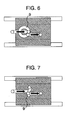
- the second cut-off part 9 may be circular as shown in Fig. 6 although it is straight in this embodiment.
- the circular second cut-off part 9 enables the position of the second cut-off part 9 to be easily recognized by the CCD camera, thereby it is possible to further reduce the number of pixels of the CCD camera.
- the second cut-off part 9 may be formed in a curved shape as shown in Fig. 7. In this way, it is possible to form the second cut-off part 9 in a curved shape.
- the second cut-off part 9 shown in Fig. 7 is formed in a waveform shape.
- the curved second cut-off part 9 allows for easy recognition by the CCD camera, as in the case of the circular second cut-off part.
- Fig. 8 is a perspective view illustrating a resistance adjusting device for carrying out resistance adjustment.
- the resistance adjusting device shown in Fig. 8 is adapted to carry out the final resistance adjustment.
- the preliminary resistance adjustment has been already completed for the electronic circuit board 1 itself with the use of an additional preliminary resistance adjusting device.
- the preliminary resistance adjusting device for carrying out the preliminary resistance adjustment which is basically similar to the final resistance adjusting device as shown in Fig. 8, comprises a laser irradiation aperture for irradiating a laser beam, and a drive portion for swinging the laser irradiation aperture for scanning, and is adapted to take up a position of the end part of the first cut-off part in the form of coordinates.
- the second cut-off part 9 may be formed while the position of the end part of the first cut-off part 8 is confirmed actually by a displacement sensor. However, even though the displacement sensor is not present, by taking up the motion of the drive portion in the form of coordinates, the coordinates of the first cut-off part 8 can be stored in memory. It is noted that since the electronic circuit board 1 is held at the same position until the second cut-off part 9 is formed after the formation of the first cut-off part 8, the coordinates of the end part of the first cut-off part 8 are never deviated.
- the electronic circuit board 1 for which the preliminary resistance adjustment has been completed is attached to a housing which is the outer shell of the air-flow sensor as a product, and thereafter, the final resistance adjustment is carried out therefor with the use of the resistance adjusting device which is shown in Fig. 8.
- This resistance adjusting device is composed of a carrier bed 12 on which the air-flow sensor before the final adjustment is set and which serves as a carrier part in a product introduction portion 11, and a moving means 13a such as a conveyer whose displacement value is automatically controlled, for automatically conveying the air-flow sensor in the direction of the arrow (from the right to the left side in Fig. 8).
- the air-flow sensor When the air-flow sensor is moved up to a position in front of an initial characteristic measuring portion 14 by the moving means 13a, the air-flow sensor is automatically lifted up onto the initial characteristic measuring portion 14 by means of a mechanical member such as an arm (which is not shown). Thereafter, a vacuum pressure is effected in the initial characteristic measuring portion 14 by means a vacuum generating unit 15, and then, an air flow rate is measured by the air-flow sensor in order to obtain a detection error. The thus obtained detection error is stored in a final resistance adjustment control portion which is not shown and which is installed in the resistance adjusting device.
- the air-flow sensor for which an initial characteristic is measured by the initial characteristic measuring portion 14 is returned to the original carrier bed 12, and is then moved to a laser irradiating portion 16 by means of the moving means 13a.
- the laser irradiating portion 16 is constituted so as to carry out scanning in both X-axial direction and Y-axial direction by a drive portion incorporated in the laser irradiating portion 16, and a CCD camera 17 serving as an image recognizing portion is mounted on one side of the laser irradiating portion 16.
- This CCD camera 17 is located at a position distance from the laser irradiating portion 16 so as to prevent affection by the laser beam, and is adapted to recognize an image which is reflected by a mirror.
- the air-flow sensor When the air-flow sensor is moved to a position in front of the laser irradiating portion 16 by means of the moving means 13a, the position of the cross-point B between the first cut-off part 8 and the second cut-off part 9 is recognized by the CCD camera 17. Further, the length of the third cut-off part 10 is calculated from a detection error which has been stored in the final resistance adjustment control portion and which is obtained from the initial characteristic.
- the laser irradiating portion 16 is swung for scanning by the drive portion, while a laser is excited by a laser energizing portion 18 provided adjacent to the laser irradiating portion 16 in order to irradiate a laser beam so as to form the third cut-off part 10.
- the CCD camera 17 also recognizes an edge part corresponding to the end part of the resistance film 3, and accordingly, the final resistance adjustment control portion sets the length between the edge part of the resistance film 3 and the third cut-off part 10 to be larger than a predetermined value with which the resistance film 3 can be prevented from cracking.
- the third cut-off part 10 is cut off by a length which has been obtained from the initial characteristic. If the length between the edge part of the resistance film 3 and the third cut-off part 10 (the point F) is not greater than the predetermined value with which the resistance film is prevented from cracking, it is determined that the air-flow sensor is defective, and accordingly, the resistance adjustment is ceased.
- the air-flow sensor for which the final resistance adjustment has been completed is shifted into a product discharge portion 19 by means of a mechanical member such as an arm (which is not shown), then is automatically moved in the direction of the arrow (from the left side to the right side in Fig. 8) by a moving means 13b such as a conveyer. That is, the air-flow sensor can be finally delivered as a finished product.
- the final resistance adjustment is carried out through a series of steps as stated above. It is noted that a plurality of air-flow sensors can be set up on the product introduction portion 11 and the product discharge portion 19, and accordingly, the resistance adjustment can be carried out for a plurality of air-flow sensors, successively.
- the resistance adjustment device can be controlled through a control panel 20, and the measurement for a resistance value and the control of the laser coordinate axes can be carried out by an equipped computer 21.
- the second cut-off part serving as a marker is formed in a direction different from the cutting-off direction of the first cut-off part, in connection with the first cut-off part at a position substantially at the end part of the latter, and accordingly, the position of the cross point between the first cut-off part and the second cut-off part can be readily recognized according to a lighting adjustment.
- a relatively inexpensive device without a risk of instability of a resistance value which is caused by cracking of the resistance film.
- the third cut-off part is cut off from the second cut-off part toward the end part of the resistance film, the second cut-off part and the third cut-off part are connected to each other with no gap therebetween, thereby it is possible to prevent the resistance value from being changed due to cracking of a remaining part therebeween.
- the position of the first cut-off part is stored in memory, and the second cutting-off step is carried out in accordance with the stored position, thereby it is possible to surely connect the second cut-off part to the first cut-off part substantially at the position of the end part of the latter.
- the resistance film is cut while coordinate data is held in the computer until the second cut-off part is formed after the formation of the first cut-off part, it is possible to correct the coordinates at any time even though the electronic circuit board is slipped during the cutting of the resistance film.
- a laser process or a sand blast process may be used. With the use of these processes, an extremely thin cut-off part can be formed in the resistance film, and accordingly very fine resistance adjustment can be made.
- the resistance adjusting element in the above-mentioned embodiment is composed of a first cut-off part which extends in the resistance film from one end and to the other end in the width direction in which the conductors are opposed to each other, and a second cut-off part which extends in a direction different from the cutting-off direction of the first cut-off part so as to cross the first cut-off part substantially at the position of the end part of the first cut-off part, and accordingly, the position of the cross point between the first cut-off part and the second cut-off part can be readily recognized according to a lighting adjustment, thereby it is possible to use a relatively inexpensive device for carrying out resistance adjustment.
- the third cut-off part is formed, leaving a part having a predetermined width remained between the second cut-off part and the other widthwise end part of the resistance film, thereby it is possible to prevent the resistance from being unstable due to cracking of the resistance film.
- the third cut-off part in the resistance adjusting element in the above-mentioned embodiment extends in the resistance film from the second cut-off part toward the other end in the width direction of the resistance film in which the conductors are opposed to each other, and accordingly, the second cut-off part and the third cut-off part are connected to each other with no gap being remained therebetween, thereby it is possible to prevent the resistance from being changed due to clacking of the remaining part.
- the second cut-off part in the resistance film is cut off in a direction substantially orthogonal to the width direction of the resistance film in which the conductors are opposed to each other.
- the first cut-off part and the second cut-off part are formed in a T-shape so that the second cut-off part is connected to the end part of the first cut-off part, and accordingly, no acute angle part is formed in the resistance film.
- first cut-off part and the third cut-off part in the resistance adjustment element in the above-mentioned embodiment are formed substantially in the same direction which is the width direction of the resistance film in which the conductors are opposed to each other, and accordingly, no acute angle part is formed in the resistance film 3.
- variation in resistance caused due to cracking of the resistance film can be reduced as possible as it can.
- the first cut-off part and the third cut-off part in the resistance adjustment element may be connected through the intermediary of the second cut-off part, being shifted from each other in the direction in which the second cut-off part extends, and accordingly, even though the first cut-off part and the third cut-off part are shifted from each other, they can be communicated with each other through the intermediary of the second cut-off part.
- the intermediary of the second cut-off part may be connected through the intermediary of the second cut-off part, being shifted from each other in the direction in which the second cut-off part extends, and accordingly, even though the first cut-off part and the third cut-off part are shifted from each other, they can be communicated with each other through the intermediary of the second cut-off part.
- the first cut-off part and the third cut-off part in the resistance adjusting element are connected to each other by way of the second cut-off part so as to define a straight line, and accordingly, the resistance adjustment can be made in a narrow range.
- the second cut-off part in the resistance adjusting element is shorter than the first cut-off part, and therefore, the cracking can be prevented as possible as it can.
- the use of a laser beam or the like can be minimized.
- the second cut-off part in the resistance adjusting element is cut off in a circular or curved shape, thereby it is possible to readily recognize the position of the second cut-off part.
- the resistance adjusting device in the above-mentioned embodiment is composed the image recognizing portion for recognizing the second cut-off part in the preliminary resistance adjustment including the formation of the first cut-off part formed in the resistance film and the second cut-off part which crosses the first cut-off part substantially at the position of the end part of the latter, and further, the third cut-off part is formed in the resistance film, being based upon the position of the second cut-off part recognized by the image recognizing portion and a measured initial characteristic, and accordingly, the resistance adjustment can be made in a relatively inexpensive manner. Further, it is possible to cut off the third cut-off part substantially from the position of the end part of the first cut-off part.
- the resistance adjustment device in the above-mentioned embodiment carries out such control that the distance between the third cut-off part and the end part of the resistance film is prevented from being not less than a predetermined value, and accordingly, it is possible to prevent occurrence of such a problem that the resistance film is cracked so as to cause no current running.
- the present invention can be applied to any of electronic circuit boards having a use purpose similar to the above-mentioned embodiment although explanation has been made of the electronic circuit board used in an air-flow sensor in the above-mentioned embodiment.
- the second cut-off part and the third cut-off part are connected to each other, the second cut-off part and the third cut-off part may not be connected to each other if the space between the second cut-off part and the third cut-off part which can prevent the resistance film from cracking can be left in the resistance film.
- the third cut-off part may be formed in a direction different from the direction of the first cut-off part although the first cut-off part and the third cut-off part are formed in the same direction in the above-mentioned embodiment. Further, it is not necessary to cross the first cut-off part and the second cut-off part, orthogonal to each other, that is, the second cut-off part may be inclined to a line perpendicular to the first cut-off part.
Landscapes
- Engineering & Computer Science (AREA)
- Microelectronics & Electronic Packaging (AREA)
- Physics & Mathematics (AREA)
- Optics & Photonics (AREA)
- Plasma & Fusion (AREA)
- Manufacturing & Machinery (AREA)
- Apparatuses And Processes For Manufacturing Resistors (AREA)
- Parts Printed On Printed Circuit Boards (AREA)
- Non-Adjustable Resistors (AREA)
Applications Claiming Priority (1)
| Application Number | Priority Date | Filing Date | Title |
|---|---|---|---|
| JP2006228542A JP4311421B2 (ja) | 2006-08-25 | 2006-08-25 | 抵抗調整方法 |
Publications (2)
| Publication Number | Publication Date |
|---|---|
| EP1892733A2 true EP1892733A2 (de) | 2008-02-27 |
| EP1892733A3 EP1892733A3 (de) | 2009-12-23 |
Family
ID=38754619
Family Applications (1)
| Application Number | Title | Priority Date | Filing Date |
|---|---|---|---|
| EP07015619A Withdrawn EP1892733A3 (de) | 2006-08-25 | 2007-08-08 | Verfahren, Element und Vorrichtung zur Regulierung des Widerstands |
Country Status (3)
| Country | Link |
|---|---|
| US (1) | US7439846B2 (de) |
| EP (1) | EP1892733A3 (de) |
| JP (1) | JP4311421B2 (de) |
Families Citing this family (3)
| Publication number | Priority date | Publication date | Assignee | Title |
|---|---|---|---|---|
| CN102609004B (zh) * | 2012-03-08 | 2014-07-23 | 台达电子企业管理(上海)有限公司 | 电学参数调节装置以及调节方法 |
| JP6618248B2 (ja) * | 2014-10-24 | 2019-12-11 | Koa株式会社 | 抵抗器およびその製造方法 |
| US10912199B1 (en) * | 2019-10-03 | 2021-02-02 | Kioxia Corporation | Resistive PCB traces for improved stability |
Citations (2)
| Publication number | Priority date | Publication date | Assignee | Title |
|---|---|---|---|---|
| JPH0945515A (ja) | 1995-07-31 | 1997-02-14 | Matsushita Electric Ind Co Ltd | トリミング方法 |
| US6148502A (en) | 1997-10-02 | 2000-11-21 | Vishay Sprague, Inc. | Surface mount resistor and a method of making the same |
Family Cites Families (5)
| Publication number | Priority date | Publication date | Assignee | Title |
|---|---|---|---|---|
| US5198794A (en) * | 1990-03-26 | 1993-03-30 | Matsushita Electric Industrial Co., Ltd. | Trimmed resistor |
| US5258738A (en) * | 1991-04-16 | 1993-11-02 | U.S. Philips Corporation | SMD-resistor |
| US6462304B2 (en) * | 1997-07-22 | 2002-10-08 | Rohm Co., Ltd. | Method of laser-trimming for chip resistors |
| JP4239280B2 (ja) * | 1999-03-23 | 2009-03-18 | パナソニック株式会社 | 抵抗器およびその製造方法 |
| US6951995B2 (en) * | 2002-03-27 | 2005-10-04 | Gsi Lumonics Corp. | Method and system for high-speed, precise micromachining an array of devices |
-
2006
- 2006-08-25 JP JP2006228542A patent/JP4311421B2/ja not_active Expired - Fee Related
-
2007
- 2007-08-07 US US11/834,815 patent/US7439846B2/en active Active
- 2007-08-08 EP EP07015619A patent/EP1892733A3/de not_active Withdrawn
Patent Citations (2)
| Publication number | Priority date | Publication date | Assignee | Title |
|---|---|---|---|---|
| JPH0945515A (ja) | 1995-07-31 | 1997-02-14 | Matsushita Electric Ind Co Ltd | トリミング方法 |
| US6148502A (en) | 1997-10-02 | 2000-11-21 | Vishay Sprague, Inc. | Surface mount resistor and a method of making the same |
Also Published As
| Publication number | Publication date |
|---|---|
| US7439846B2 (en) | 2008-10-21 |
| US20080048824A1 (en) | 2008-02-28 |
| JP2008053481A (ja) | 2008-03-06 |
| EP1892733A3 (de) | 2009-12-23 |
| JP4311421B2 (ja) | 2009-08-12 |
Similar Documents
| Publication | Publication Date | Title |
|---|---|---|
| US5690846A (en) | Laser processing method | |
| US6875950B2 (en) | Automated laser trimming of resistors | |
| US7181089B2 (en) | Method and apparatus for searching for fiducial marks, and method of detecting positions of the fiducial marks | |
| US6256876B1 (en) | Method and device for mounting electronic components | |
| US7439846B2 (en) | Resistance adjusting method and resistance adjusting element and resistance adjusting device | |
| CN111684550A (zh) | 嵌入式电阻的直接印刷 | |
| EP0478170A2 (de) | Aufbringen einer Lötpaste | |
| US5535903A (en) | Method for breaking conducting path formed on or in printed-circuit board and laser system for using the method | |
| JPH11309593A (ja) | レーザ位置決め加工方法及び装置 | |
| JP4901077B2 (ja) | 加工上の基準点の位置決定方法およびレーザ加工機 | |
| JP3469991B2 (ja) | ペースト塗布機 | |
| JP2001315299A (ja) | スクリーン印刷におけるスクリーンマスクの位置合わせ方法 | |
| JP2004200618A (ja) | レーザトリミング装置 | |
| JPH0918116A (ja) | 回路基板作成装置 | |
| US6593066B2 (en) | Method and apparatus for printing patterns on substrates | |
| US20260092356A1 (en) | Coating for donor substrate in laser induced forward transfer repair of substrate process | |
| JPH08219736A (ja) | 電子部品トリミング方法 | |
| JPH02298095A (ja) | 直接描画装置における基板表面計測方法 | |
| JPH0911694A (ja) | 回路基板欠陥補修装置 | |
| JP4326064B2 (ja) | 電子部品認識装置及び方法、並びに電子部品認識装置を備えた電子部品実装機 | |
| WO2026074337A1 (en) | Coating for donor substrate in laser induced forward transfer repair of substrate process | |
| JP4696945B2 (ja) | 配線基板修正方法及び配線基板修正装置 | |
| JP2827577B2 (ja) | トリミング装置 | |
| JPH05226815A (ja) | ワイヤ位置決め装置 | |
| JPH10145096A (ja) | 電子部品の装着方法及び装置 |
Legal Events
| Date | Code | Title | Description |
|---|---|---|---|
| PUAI | Public reference made under article 153(3) epc to a published international application that has entered the european phase |
Free format text: ORIGINAL CODE: 0009012 |
|
| AK | Designated contracting states |
Kind code of ref document: A2 Designated state(s): AT BE BG CH CY CZ DE DK EE ES FI FR GB GR HU IE IS IT LI LT LU LV MC MT NL PL PT RO SE SI SK TR |
|
| AX | Request for extension of the european patent |
Extension state: AL BA HR MK YU |
|
| 17P | Request for examination filed |
Effective date: 20090420 |
|
| PUAL | Search report despatched |
Free format text: ORIGINAL CODE: 0009013 |
|
| AK | Designated contracting states |
Kind code of ref document: A3 Designated state(s): AT BE BG CH CY CZ DE DK EE ES FI FR GB GR HU IE IS IT LI LT LU LV MC MT NL PL PT RO SE SI SK TR |
|
| AX | Request for extension of the european patent |
Extension state: AL BA HR MK RS |
|
| RIC1 | Information provided on ipc code assigned before grant |
Ipc: H05K 1/16 20060101ALI20091118BHEP Ipc: H01C 17/242 20060101AFI20091118BHEP |
|
| AKX | Designation fees paid |
Designated state(s): DE FR |
|
| STAA | Information on the status of an ep patent application or granted ep patent |
Free format text: STATUS: THE APPLICATION HAS BEEN WITHDRAWN |
|
| 18W | Application withdrawn |
Effective date: 20150220 |