EP1892829B1 - Amplificateur à gain variable et dispositif de source d'alimentation électrique ca l'utilisant - Google Patents
Amplificateur à gain variable et dispositif de source d'alimentation électrique ca l'utilisant Download PDFInfo
- Publication number
- EP1892829B1 EP1892829B1 EP06783082.8A EP06783082A EP1892829B1 EP 1892829 B1 EP1892829 B1 EP 1892829B1 EP 06783082 A EP06783082 A EP 06783082A EP 1892829 B1 EP1892829 B1 EP 1892829B1
- Authority
- EP
- European Patent Office
- Prior art keywords
- current
- initial stage
- base
- power supply
- stage transistor
- Prior art date
- Legal status (The legal status is an assumption and is not a legal conclusion. Google has not performed a legal analysis and makes no representation as to the accuracy of the status listed.)
- Ceased
Links
- 230000005669 field effect Effects 0.000 claims description 5
- 238000010586 diagram Methods 0.000 description 16
- 239000003990 capacitor Substances 0.000 description 4
- 238000012886 linear function Methods 0.000 description 2
- XUIMIQQOPSSXEZ-UHFFFAOYSA-N Silicon Chemical compound [Si] XUIMIQQOPSSXEZ-UHFFFAOYSA-N 0.000 description 1
- 238000001514 detection method Methods 0.000 description 1
- 230000000694 effects Effects 0.000 description 1
- 230000005685 electric field effect Effects 0.000 description 1
- 238000000034 method Methods 0.000 description 1
- 229920006395 saturated elastomer Polymers 0.000 description 1
- 229910052710 silicon Inorganic materials 0.000 description 1
- 239000010703 silicon Substances 0.000 description 1
- 239000000758 substrate Substances 0.000 description 1
Images


Classifications
-
- H—ELECTRICITY
- H03—ELECTRONIC CIRCUITRY
- H03G—CONTROL OF AMPLIFICATION
- H03G1/00—Details of arrangements for controlling amplification
- H03G1/0005—Circuits characterised by the type of controlling devices operated by a controlling current or voltage signal
- H03G1/0017—Circuits characterised by the type of controlling devices operated by a controlling current or voltage signal the device being at least one of the amplifying solid-state elements
- H03G1/0023—Circuits characterised by the type of controlling devices operated by a controlling current or voltage signal the device being at least one of the amplifying solid-state elements in emitter-coupled or cascode amplifiers
-
- H—ELECTRICITY
- H03—ELECTRONIC CIRCUITRY
- H03F—AMPLIFIERS
- H03F3/00—Amplifiers with only discharge tubes or only semiconductor devices as amplifying elements
- H03F3/45—Differential amplifiers
- H03F3/45071—Differential amplifiers with semiconductor devices only
- H03F3/45076—Differential amplifiers with semiconductor devices only characterised by the way of implementation of the active amplifying circuit in the differential amplifier
- H03F3/4508—Differential amplifiers with semiconductor devices only characterised by the way of implementation of the active amplifying circuit in the differential amplifier using bipolar transistors as the active amplifying circuit
- H03F3/45085—Long tailed pairs
Definitions
- the present invention relates to a variable gain amplifier and an alternating current (AC) power-supply device including the amplifier.
- a resistor is inserted in series to the emitter of each of initial stage transistors Q1 and Q2. This arrangement may reduce the non-linear distortion, but cannot completely eliminate the distortion.
- FIG. 7 is a circuit diagram of multiplier circuit 5001.
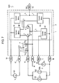
- Integrated circuit (IC) 1 includes transconductance amplifier 2 and a pair of PN junction elements 4, and includes seven terminals, that is, power-supply terminal 1A (+Vcc), power-supply terminal 1B (-Vcc), input terminal 1C (INV), input terminal 1D (NI), input terminal 1E (BIAS), input terminal 1F (DB), and output terminal 1G (OUT).
- Constant-current supply 101 ID is connected to input terminal 1F.
- Constant power supply 103 (1/2I D ) outputting a 1/2 of the current from constant current supply 101 and signal input power supply (IX) are connected to input terminal 1C.
- Current Iout is output from output terminal 1G.
- Amplifier 2 includes four current mirrors 5A to 5D and two initial stage transistors Q1 and Q2. Pair of PN junction elements 4 are configured by two diodes D 1 and D 2 .
- multiplier circuit 5001 An operation of multiplier circuit 5001 will be described below.
- V BE Voltage V BE between the base and emitter of a transistor is expressed by the following equation with emitter current I E , saturated current I SAT and collector current Ic. Base current I B is much smaller than a collector current, hence providing I E ⁇ I C .
- Forward direction voltage VD of a diode is expressed by the following equation with forward direction current ID of the diode.
- V D V T • ln I D / I SAT
- Equation 7 Based upon Equation 7, when current I D is constant, the product of input currents Ix and Iy is obtained from output terminal 1G as current Iout. When input current Iy is constant, the dividend obtained by dividing input current Ix by input current I D is obtained as output current Iout. Equation 7 includes no term of exponential function, and includes only terms of linear function, hence allowing multiplier circuit 5001 to generate no linear distortion in principle. Input current Ix and input current Iy are used as a signal input and a control input, respectively, thereby providing a variable gain amplifier generating no linear distortion in principle.
- Multiplier circuit 5001 requires input terminal 1F for inputting a current to IC 1 from constant current supply 101, hence causing IC 1 to include seven terminals.
- An IC generally includes an even number of terminals, thus IC 1 necessarily includes a package having eight terminals.
- the IC package includes eight pins or six pins.
- an area occupied by pads used for connecting terminals is greater than an area of a chip implementing circuit 5001.
- the area of the pads corresponding to the number of terminals influences the area of the chip, and is greatly reflected in the yield and costs.
- Document EP 0 176 971 A2 discloses a current controlled amplifier comprising a two-stage differential amplifier and three current mirror circuits. The gain of the amplifier is a adjusted by a current source.
- a variable gain amplifier includes first and second power supply terminals arranged to be connected to a power supply, a transconductance amplifier, first and second PN junction elements, a voltage drop element, first and second resistors, a current-generating transistor, and a current mirror.
- the transconductance amplifier outputs a current corresponding to a difference between a potential of a base of the first initial stage transistor and a potential of a base of the second initial stage transistor.
- An emitter of the second initial stage transistor is connected to the emitter of the first initial stage transistor at a node.
- Each of the first and second PN junction elements has a first end connected to the base of the first initial stage transistor and a second end.
- the voltage drop element is connected between the second end of the first PN junction element and the first power supply terminal.
- the first resistor is connected between the base of the second initial stage transistor and a first signal source which is a voltage source.
- the current-generating transistor has a collector connected to the base of the first initial stage transistor and a base connected to the first signal source.
- the second resistor is connected between the emitter of the current-generating transistor and the second power supply terminal.
- the current mirror is connected to the node, and allows a current to flow to the node, the current being identical to a current flowing from the second signal source which is a current source.
- This variable gain amplifier generates no non-linear distortion, and has a small size.
- Fig. 1 is a circuit diagram of a variable gain amplifier 1001 including a multiplier circuit in accordance with an exemplary embodiment of the present invention.
- components identical to those of conventional multiplier circuit 5001 shown in Fig. 7 are denoted by the same reference numerals, and their description will be omitted.
- variable gain amplifier 1001 shown in Fig. 1 does not require input terminal 1F.
- integrated circuit (IC) 10 includes transconductance amplifier 2, voltage drop element 3, and a pair of PN junction elements 4A and 4B.
- IC 10 includes six 6 terminals, that is, power supply terminal 10A (Vcc), input terminal 10C (INV), input terminal 10D (NI), input terminal 10E (BIAS), output terminal 10G (OUT), and power supply terminal 10B (GND) functioning as a ground.
- Power supply Vcc has an end Vcc1 connected to power supply terminal 10A, and has an end Vcc2 connected to power supply terminal 10B.
- PN junction elements 4A and 4B are implemented by diodes D 1 and D 2 , respectively.
- An end 3A of voltage drop element 3 is connected to power supply terminal 10A (Vcc) so that a voltage dropping by a voltage V 3 from the voltage of power supply terminal 10A appears at an end 3B of voltage drop element 3.
- Respective anodes of diodes D 1 and D 2 are connected to the end 3B of voltage drop element 3.
- the cathode of diode D 1 is connected to input terminal 10C (INV).
- the collector of current-generating transistor Tr 1 is connected to input terminal 10C, and the emitter of current-generating transistor Tr 1 is connected to an end R 10 A of resistor R 10 .
- An end R 10 B of resistor R 10 is connected to power supply Vcc (power supply terminal 10B). Voltage Vs of signal source 501 is applied to the base of current-generating transistor Tr1. Signal source 501 is biased by DC bias Vb. Input terminal 10D (NI) is connected to signal source 501 via resistor R 11 .
- a potential of a node where diode D 1 and the collector of current-generating transistor Tr 1 is connected and a potential of a node where resistor R 11 and diode D 2 are connected are input as differential inputs to transconductance amplifier 2.
- the current flowing in a common emitter of initial stage transistors Q 1 and Q 2 providing an initial stage differential amplifier of transconductance amplifier 2 is controlled via current mirror 5C by current Ic of signal source 502, a current source.
- Transconductance amplifier 2 includes initial stage transistors Q1 and Q2.
- the emitter of initial stage transistor Q1 is connected to the emitter of initial stage transistor Q2 at a node 2P.
- Current Iout corresponding to a difference between a potential of the base of initial stage transistor Q1 and a potential of the base of initial stage transistor Q2 is output from output terminal 10G.
- Diode D 1 i.e., PN junction element 4A
- Diode D 2 i.e., PN junction element 4B
- the cathodes of diodes D 1 and D 2 are connected to each other.
- Voltage drop element 3 is connected between the cathodes of diodes D 1 and D 2 and power supply terminal 10A.
- Resistor R 11 is connected between the base of initial stage transistor Q2 and signal source 501, a voltage source.
- the collector of current-generating transistor Tr 1 is connected to the base of initial stage transistor Q 1 .
- the base of current-generating transistor Tr 1 is connected to signal source 501.
- Resistor R 10 is connected between power supply terminal 10B and the emitter of current-generating transistor Tr 1 .
- Current mirror 5C is connected to the node 2P to cause a current identical to current Ic flowing from signal source 501, the current source, to flow in the node 2P. That is, current mirror 5C makes the sum of currents flowing through the emitters of initial stage transistors Q1 and Q2 equal to current Ic.
- variable gain amplifier 1001 While the sum (current I D ) of currents I D1 and I D2 flowing in diodes D 1 and D 2 is kept constant, an input signal is added to current I D1 , and current Ic is applied to the BIAS terminal.
- current I D current of currents I D1 and I D2 flowing in diodes D 1 and D 2
- current Ic current Ic is applied to the BIAS terminal.
- conventional multiplier circuit 5001 shown in Fig. 7 according to Equations 1 to 7, when ID is constant, the product of input currents Is and Ic is obtained from output terminal 10G as current Iout, thus providing a multiplying function.
- AC alternating-current
- current-generating transistor Tr 1 and resistors R 10 and R 11 input voltage Vs of signal source 501 to input terminals 10C and 10D as input current Is.
- Currents I D1 and I D2 flowing in diodes D 1 and D 2 have phases opposite to each other.
- variable gain amplifier 1001 Since (I D1 +I D2 ) is constant regardless of voltage Vs, the gain of variable gain amplifier 1001 shown in Fig. 1 is determined by current Ic to be input to input terminal 10E. Since this equation includes only the term of linear function, variable gain amplifier 1001 does not generate any non-linear distortion in principle. That is, the ratio of current Iout output from output terminal 10G to voltage Vs of signal source 501 of transconductance amplifier 2 is variable according to current Ic flowing from signal source 502.
- Diodes D 1 and D 2 and initial stage transistors Q 1 and Q 2 need to be kept at the same temperature so as to perform the multiplying function accurately, and are preferably arranged on a single silicon substrate as an IC.
- IC 10 has six terminals, and accommodated in a package identical to that of a small-signal transistor, which is the smallest IC, effectively meeting demands for thin and small-size electronic apparatuses.
- IC 10 includes the six terminals, and has an area of a chip much smaller than that of an IC including eight pins, being advantageous from the viewpoints of yield and cost.
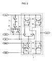
- Fig. 2 is a circuit diagram of integrated circuit 10 for showing transconductance amplifier 2 and voltage drop element 3.
- diodes D 1 and D 2 of PN junction elements 4A and 4B are configured by an IC, transistors with diode-connection, i.e., with the collector and the base of each of the transistors being connected to each other, are actually used as diodes D 1 and D 2 .
- Transconductance amplifier 2 is configured by four current mirrors 5A to 5D and two initial stage transistors Q 1 and Q 2 .
- Each of current mirrors 5A to 5D is configured by three transistors Q 5 , Q 6 , and Q 7 .
- Voltage drop element 3 applies appropriate potentials input to transconductance amplifier 2, that is, to the bases of initial stage transistors Q 1 and Q 2 .
- Element 3 includes two transistors Q 8 and Q 9 that utilize a forward-direction voltage drop of diode and resistor R 3 as an impedance element connected between transistors Q 8 and Q 9 .
- Voltage drop element 3 may be an element, such as a zener diode, that drops a voltage.
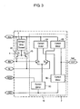
- Fig. 3 is another circuit diagram of integrated circuit 10. As shown in Fig. 3 , PN junction elements 4A and 4B are implemented by a PN junction between the base and emitter of each of transistors Q 3 and Q 4 .
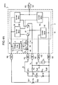
- Fig. 4A is a circuit diagram of variable gain amplifier 1001A according to the embodiment.
- Variable gain amplifier 1001A includes field effect transistor FET 1 instead of current-generating transistor Tr1 of variable gain amplifier 1001 shown in Fig. 1 .
- the drain, the gate and the source of field effect transistor FET 1 are connected instead of the collector, the base, and the emitter of current-generating transistor Tr 1 , respectively.
- Fig. 4B is a circuit diagram of another IC 110 of variable gain amplifier 1001 according to the embodiment.
- IC 110 has an arrangement of voltage drop element 3, PN junction elements 4A and 4B, current-generating transistor Tri, and resistor R 10 is opposite to that of IC 10 shown in Fig. 1 , and the other portions are arranged in the same manner. That is, the anode of diode D 1 is connected to input terminal 110C and the base of initial stage transistor Q 1 , and the anode of diode D 2 is connected to input terminal 110D and the base of transistor Q 2 .
- the cathodes of diode D1 and D2 are connected to end 3A of voltage drop element 3. End 3B of voltage drop element 3 is connected to power supply terminal 110B connected to the ground.
- IC 110 provides the same effects as those of IC 10 shown in Fig. 1 .
- resistor R 12 for adjusting offset is omitted.
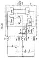
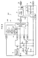
- Fig. 5 is a circuit diagram of showing alternating-current (AC) constant voltage power supply device 2001 including variable gain amplifier 1001 according to the embodiment.
- Wave-form generator 11 generates a waveform of an AC voltage to be desirably obtained as an output. In order to generate an AC voltage having a sine wave form, wave-form generator 11 generates a sine wave voltage. The sine wave voltage output from wave-form generator 11 is applied to current-generating transistor Tr 1 and resistor R 11 so that sine wave current Iout is obtained from output terminal 10G of IC 10. Resistor R 17 converts sine wave current Iout output from IC 10 into a sine wave voltage. This sine wave voltage is input to power amplifier 12.
- the sine wave voltage input to power amplifier 12 is amplified, and is applied to primary coil N 1 of transformer 13 for driving transformer 13.
- a sine wave AC voltage is output from secondary coil N 2 of transformer 13 via output terminals 13A and 13B.
- Tertiary coil N 3 of the transformer generates an AC voltage in proportion to the output AC voltage, and the AC voltage is converted into a pulsating voltage by a rectifier circuit configured by diodes D 10 , D 11 , D 12 , and D 13 and resistor R 19 .
- Resistor R 19 is a dummy load resistor for obtaining an appropriate pulsating voltage.
- the pulsating voltage is smoothed by a low pass filter configured by resistor R 14 and capacitor C 10 , providing a direct-current (DC) voltage in proportion to the AC voltage output from output terminals 13A and 13B. That is, the rectifier circuit and the low pass filter provides output voltage detector 14 that detects the AC voltage output from output terminals 13A and 13B, and generates the DC voltage as a detection signal.
- DC direct-current
- Comparator OP 1 compares the DC voltage with reference voltage Vref, and outputs a voltage corresponding to a difference obtained by subtracting the DC voltage from reference voltage Vref.
- the output voltage is input to input terminal 10E of IC 10 as current Ic via resistor R 13 . If the DC voltage is lowered to increase the difference from reference voltage Vref, the voltage output from by comparator OP1 increases as to allow variable gain amplifier 1001 to increase the AC voltage output from output terminals 13A and 13B. The AC voltage output through such a negative feedback is stabilized. If the output voltage is changed, reference voltage Vref is changed, or the voltage output from output voltage detector 14 is voltage-divided and changed.
- Resistors R 15 and R 16 and capacitor C 11 constitute a phase compensating circuit used for stably performing the negative feedback.
- Output voltage detector 14, comparator OP 1 , reference voltage Vref, resistors R 13 , R 15 , and R 16 , and capacitor C 11 provide a feedback circuit that feedbacks the amplitude of the output AC voltage as current Ic.
- Fig. 6 is a circuit diagram of AC constant current power-supply device 3001 in accordance with this embodiment.
- Resistor R 18 generates an AC voltage in proportion to an AC current flowing in output terminals 13A and 13B.
- the generated AC voltage is converted into a DC voltage by a rectifier circuit including diodes D 15 and D 14 and a low pass filter including capacitor C 10 and resistor R 14 . That is, the rectifier circuit and the low pass filter provides output current detector 15 for detecting an AC current flowing in output terminals 13A and 13B, and outputs a DC voltage in proportional to the current.
- comparator OP 1 outputs a voltage corresponding to a difference obtained by subtracting the DC voltage from reference voltage Vref.
- IC 10 drives transformer 13 via power amplifier 12 in accordance with the voltage output from comparator OP 1 so that a DC voltage output from output current detector 15 becomes identical to reference voltage Vref. This operation stabilizes the current flowing through output terminals 13A and 13B as a constant current.
- Resistor R 19 is a dummy load resistor for setting a pulsating voltage output from the rectifier circuit to an appropriate level.
- Output current detector 15, comparator OP 1 , reference voltage Vref, and resistor R 19 provide a feedback circuit that feedbacks the amplitude of the output AC voltage as current Ic.
- Variable gain amplifier 1001 in accordance with the embodiment provides AC power supply devices 2001 and 3001 outputting a constant voltage and a constant current which are variable, respectively.
- variable gain amplifier generates no non-linear distortion, and has a small size, being applicable to an AC power supply device outputting a variable current.
- This, variable gain amplifier is useful for various power supply devices and power systems, such as uninterruptive power supply devices and electrophotographic processing power supply devices for photocopy machines, printers.
Landscapes
- Engineering & Computer Science (AREA)
- Power Engineering (AREA)
- Amplifiers (AREA)
- Control Of Amplification And Gain Control (AREA)
Claims (5)
- Amplificateur à gain variable comprenant :une première borne d'alimentation (10A) disposée de manière à être connectée à une première extrémité d'une alimentation ;une deuxième borne d'alimentation (10B) disposée de manière à être connecté à une deuxième extrémité de l'alimentation ;un amplificateur à transconductance (2) incluant
un premier transistor d'étage initial (Q1) comprenant un émetteur, une base et un collecteur,
un deuxième transistor d'étage initial (Q2) comprenant un émetteur connecté à l'émetteur du première transistor d'étage initial (Q1) au niveau d'un noeud (2P), une base et un collecteur, et
une borne de sortie (10G) pour produire un courant correspondant à une différence entre un potentiel de la base du premier transistor d'étage initial (Q1) et un potentiel de la base du deuxième transistor d'étage initial (Q2) ;un premier élément de jonction PN (4A) ayant une première extrémité connectée à la base du premier transistor d'étage initial (Q1) et une deuxième extrémité ;un deuxième élément de jonction PN (4B) ayant une première extrémité connectée à la base du deuxième transistor d'étage initial (Q2) et une deuxième extrémité connectée à la deuxième extrémité du premier élément de jonction PN (4A) ;un élément de baisse de tension (3) connecté entre la deuxième extrémité du premier élément de jonction PN (4A) et la première borne d'alimentation (10A) ;un transistor de génération de courant (TR1) ayant un collecteur connecté à la base du premier transistor d'étage initial (Q1) et la première extrémité du premier élément de jonction PN (4A) via une première borne d'entrée (10C), une base connectée à une première source de de signal (501) et un émetteur ; etune deuxième résistance (R10) connectée entre l'émetteur du transistor de génération de courant (TR1) et la deuxième borne d'alimentation (10B), caractérisé parune première résistance (R11) connectée entre une deuxième borne d'entrée (10D) et la première source de signal (501) qui est une source de tension, la deuxième borne d'entrée (10D) étant connectée à la première extrémité du deuxième élément de jonction PN (4B) et la base du deuxième transistor d'étage initial (Q2) de sorte que le courant qui circule du collecteur du transistor de génération de courant (TR1) jusque dans la première borne d'entrée (10C) est opposé mais égal au courant circulant de la première résistance (R11) jusque dans la deuxième borne d'entrée (10D) ; etun amplificateur à transconductance (2) comprenant un miroir de courant connecté au noeud, le miroir de courant autorisant le flux d'un courant vers le noeud, le courant étant identique à un courant circulant depuis la deuxième source de signal qui est une source de courant. - Amplificateur à gain variable selon la revendication 1, où le gain, représenté par un rapport du courant de sortie provenant de la borne de sortie (10G) à une tension de la première source de signal (501) de l'amplificateur à transconductance, est variable selon le courant circulant à partir de la deuxième source de signal (502).
- Amplificateur à gain variable selon la revendication 1, comprenant en outre un circuit intégré (10) recevant le premier élément de jonction PN (4A), le deuxième élément de jonction PN (4B), l'amplificateur à transconductance (2) et le miroir de courant (5C), le circuit intégré (10) comprenant
la première borne d'entrée (10C) connecté à la base du premier transistor d'étage initial (Q1),
la deuxième borne d'entrée (10D) connecté à la base du deuxième transistor d'étage initial (Q2),
une troisième borne d'entrée (10E) qui est un noeud où le miroir de courant (5C) est connecté à la deuxième source de signal (502),
la première borne d'alimentation (10A),
la deuxième borne d'alimentation (10B), et
la borne de sortie (10G) de l'amplificateur à transconductance (2). - Amplificateur à gain variable comprenant :une première borne d'alimentation (10A) apte à être connectée à une première extrémité d'une alimentation ;une deuxième borne d'alimentation (10B) apte à être connectée à une deuxième extrémité de l'alimentation ;un amplificateur à transconductance (2) comprenantun premier transistor d'étage initial (Q1) comportant un émetteur, une base et un collecteur,un deuxième transistor d'étage initial (Q2) comportant un émetteur connecté à l'émetteur du premier transistor d'étage initial (Q1) au niveau d'un noeud (2P), une base et un collecteur, etune borne de sortie (10G) pour produire un courant correspondant à une différence entre un potentiel de la base du premier transistor d'étage initial (Q1) et un potentiel de la base du deuxième transistor d'étage initial (Q2) ;un premier élément de jonction PN (4A) ayant une première extrémité connectée à la base du premier transistor d'étage initial (Q1) et une deuxième extrémité ;un deuxième élément de jonction PN (4B) ayant une première extrémité connectée à la base du deuxième transistor d'étage initial (Q2) et une deuxième extrémité connectée à la deuxième extrémité du premier élément de jonction PN (4A) ;un élément de baisse de tension (3) connecté entre la deuxième extrémité du premier élément de jonction PN (4A) et la première borne d'alimentation (10A) ;un transistor de génération de courant à effet de champ (FET1) ayant un drain connecté à la base du premier transistor d'étage initial (Q1) et la première extrémité du premier élément de jonction PN (4A) via une première borne d'entrée (10C), une grille connectée à une première source de de signal (501) et une source; etune deuxième résistance (R10) connectée entre la source du transistor de génération de courant à effet de champ (FET1) et la deuxième borne d'alimentation (10B), caractérisé parune première résistance (R11) connectée entre une deuxième borne d'entrée (10D) et la première source de signal (501) qui est une source de tension, la deuxième borne d'entrée (10D) étant connectée à la première extrémité du deuxième élément de jonction PN (4B) et la base du deuxième transistor d'étage initial (Q2) de sorte que le courant qui circule du drain du transistor de génération de courant à effet de champ (FET1) jusque dans la première borne d'entrée (10C) est opposé mais égal au courant circulant de la première résistance (R11) jusque dans la deuxième borne d'entrée (10D) ; etl'amplificateur à transconductance (2) comprenant un miroir de courant connecté au noeud, le miroir de courant autorisant le flux d'un courant vers le noeud, le courant étant identique à un courant circulant depuis la deuxième source de signal qui est une source de courant.
- Dispositif d'alimentation à courant alternatif (AC) comprenant :l'amplificateur à gain variable selon l'une quelconque des revendications 1 à 3 ;un générateur d'onde servant de première source de signal (501) ;un amplificateur de puissance (12) amplifiant le courant de sortie provenant de la borne de sortie (10G) de l'amplificateur à transconductance (2) et produit une puissance en courant alternatif ;et un circuit à rétroaction (14) qui renvoie une amplitude de la puissance en courant alternatif comme courant circulant à partir de la deuxième source de signal.
Applications Claiming Priority (2)
| Application Number | Priority Date | Filing Date | Title |
|---|---|---|---|
| JP2005251155A JP4997730B2 (ja) | 2005-08-31 | 2005-08-31 | 可変利得増幅器およびそれを用いた交流電源装置 |
| PCT/JP2006/316853 WO2007026639A1 (fr) | 2005-08-31 | 2006-08-28 | Amplificateur à gain variable et dispositif de source d'alimentation électrique ca l'utilisant |
Publications (3)
| Publication Number | Publication Date |
|---|---|
| EP1892829A1 EP1892829A1 (fr) | 2008-02-27 |
| EP1892829A4 EP1892829A4 (fr) | 2010-02-24 |
| EP1892829B1 true EP1892829B1 (fr) | 2013-04-24 |
Family
ID=37808729
Family Applications (1)
| Application Number | Title | Priority Date | Filing Date |
|---|---|---|---|
| EP06783082.8A Ceased EP1892829B1 (fr) | 2005-08-31 | 2006-08-28 | Amplificateur à gain variable et dispositif de source d'alimentation électrique ca l'utilisant |
Country Status (5)
| Country | Link |
|---|---|
| US (1) | US7602247B2 (fr) |
| EP (1) | EP1892829B1 (fr) |
| JP (1) | JP4997730B2 (fr) |
| CN (1) | CN101223689B (fr) |
| WO (1) | WO2007026639A1 (fr) |
Families Citing this family (6)
| Publication number | Priority date | Publication date | Assignee | Title |
|---|---|---|---|---|
| TWI442688B (zh) * | 2009-12-20 | 2014-06-21 | Microsemi Corp | 電源轉換器及控制電源轉換器之方法 |
| RU2469467C1 (ru) * | 2011-10-21 | 2012-12-10 | Федеральное государственное бюджетное образовательное учреждение высшего профессионального образования "Южно-Российский государственный университет экономики и сервиса" (ФГБОУ ВПО "ЮРГУЭС") | Многокаскадный усилитель переменного тока |
| US8970302B2 (en) * | 2013-08-05 | 2015-03-03 | Power Integrations, Inc. | Operational amplifier with selective input |
| US11646720B2 (en) | 2020-11-06 | 2023-05-09 | Hong Kong Applied Science and Technology Research Institute Company Limited | Active filter for electromagnetic interference (EMI) reduction using a single connection point and a negative impedance converter with cross-coupled transistors |
| CN114035103B (zh) * | 2021-11-03 | 2024-04-16 | 苏州博创集成电路设计有限公司 | 电源系统检测装置及电源系统 |
| WO2023151105A1 (fr) * | 2022-02-09 | 2023-08-17 | Hong Kong Applied Science and Technology Research Institute Company Limited | Filtre actif pour une réduction d'interférence électromagnétique (emi) à l'aide d'un point de connexion unique et d'un convertisseur d'impédance négative avec des transistors à couplage croisé |
Family Cites Families (17)
| Publication number | Priority date | Publication date | Assignee | Title |
|---|---|---|---|---|
| US4408514A (en) * | 1976-06-25 | 1983-10-11 | Nippon Gakki Seizo Kabushiki Kaisha | Electronic musical instrument having portaments property |
| JPS59172819A (ja) * | 1983-03-19 | 1984-09-29 | Rohm Co Ltd | 利得可変増幅器 |
| CA1231441A (fr) * | 1984-07-10 | 1988-01-12 | Kazuyoshi Kuwahara | Circuit d'enregistrement a reglage automatique du courant d'enregistrement d'une tete d'enregistrement magnetique |
| JPS6175610A (ja) * | 1984-09-21 | 1986-04-18 | Toshiba Corp | トランジスタ回路 |
| DE176971T1 (de) | 1984-09-29 | 1986-11-27 | Wakamoto Pharmaceutical Co., Ltd., Tokio/Tokyo | Fuer ein thermostabiles beta-galaktosidase, kodierendes gen, dieses gen enthaltender bacillus-subtilis, das durch dieses gen kodiertes enzym und verfahren zu dessen herstellung. |
| JPH0760981B2 (ja) * | 1984-12-28 | 1995-06-28 | ロ−ム株式会社 | 電圧−電流変換回路 |
| JPH0681108B2 (ja) * | 1989-03-22 | 1994-10-12 | 株式会社東芝 | Fmステレオマルチプレックス復調回路のマトリックス回路 |
| JPH0529853A (ja) * | 1991-07-22 | 1993-02-05 | Toshiba Corp | 直線性補正回路 |
| JP3178614B2 (ja) * | 1991-10-16 | 2001-06-25 | ソニー株式会社 | 増幅回路 |
| US5497123A (en) * | 1994-12-23 | 1996-03-05 | Motorola, Inc. | Amplifier circuit having high linearity for cancelling third order harmonic distortion |
| FI106413B (fi) * | 1996-07-11 | 2001-01-31 | Nokia Mobile Phones Ltd | Lineaarisen tehovahvistimen tehonsäätöpiiri |
| JPH10126178A (ja) * | 1996-10-18 | 1998-05-15 | Nec Corp | 可変利得増幅器 |
| JPH10209813A (ja) * | 1997-01-24 | 1998-08-07 | Murata Mfg Co Ltd | 不平衡−平衡変換回路 |
| JP3772938B2 (ja) * | 1997-08-14 | 2006-05-10 | ソニー株式会社 | 利得制御回路 |
| US6084471A (en) * | 1997-12-19 | 2000-07-04 | Nokia Mobile Phones | Soft-limiting control circuit for variable gain amplifiers |
| JP2001308662A (ja) | 2000-04-27 | 2001-11-02 | Matsushita Electric Ind Co Ltd | 可変利得増幅回路 |
| JP4315095B2 (ja) * | 2004-11-04 | 2009-08-19 | パナソニック株式会社 | アナログ乗、除算回路およびそれらを用いた電力装置 |
-
2005
- 2005-08-31 JP JP2005251155A patent/JP4997730B2/ja not_active Expired - Fee Related
-
2006
- 2006-08-28 CN CN2006800259931A patent/CN101223689B/zh not_active Expired - Fee Related
- 2006-08-28 EP EP06783082.8A patent/EP1892829B1/fr not_active Ceased
- 2006-08-28 WO PCT/JP2006/316853 patent/WO2007026639A1/fr not_active Ceased
- 2006-08-28 US US11/915,018 patent/US7602247B2/en not_active Expired - Fee Related
Also Published As
| Publication number | Publication date |
|---|---|
| US20080197822A1 (en) | 2008-08-21 |
| EP1892829A4 (fr) | 2010-02-24 |
| WO2007026639A1 (fr) | 2007-03-08 |
| US7602247B2 (en) | 2009-10-13 |
| CN101223689A (zh) | 2008-07-16 |
| CN101223689B (zh) | 2012-02-01 |
| EP1892829A1 (fr) | 2008-02-27 |
| JP4997730B2 (ja) | 2012-08-08 |
| JP2007067824A (ja) | 2007-03-15 |
Similar Documents
| Publication | Publication Date | Title |
|---|---|---|
| CN112930646B (zh) | 用于调节开关电源的偏置电压的设备 | |
| CN112882524B (zh) | 带隙基准电路、对应的设备和方法 | |
| JP2001336987A (ja) | 温度検出回路およびそれを用いる液晶駆動装置 | |
| US9864389B1 (en) | Temperature compensated reference voltage circuit | |
| US7081742B2 (en) | Power supply apparatus provided with overcurrent protection function | |
| US20020113652A1 (en) | Amplifier circuit | |
| JP3360025B2 (ja) | 定電圧回路 | |
| KR20000070027A (ko) | 절대 온도에 비례하는 전압을 발생하는 장치를 포함하는 집적회로 및 전압 발생 방법 | |
| US6867644B2 (en) | Current control circuitry | |
| JP2004328640A (ja) | バイアス電流生成回路、レーザダイオード駆動回路及び光通信用送信器 | |
| GB2223904A (en) | Diamond follower with zero input offset - uses current mirror bias | |
| EP1892829B1 (fr) | Amplificateur à gain variable et dispositif de source d'alimentation électrique ca l'utilisant | |
| JP2781934B2 (ja) | 供給電流補償回路 | |
| US20250147532A1 (en) | Reference voltage generation circuit and electronic device | |
| US5920184A (en) | Low ripple voltage reference circuit | |
| US7729399B2 (en) | Semiconductor laser driving circuit less susceptible to noise interference | |
| US7071766B2 (en) | Constant voltage generating circuit | |
| EP3282581A1 (fr) | Étage tampon et circuit de commande | |
| KR20080000542A (ko) | 스위칭 레귤레이터 | |
| US20070200546A1 (en) | Reference voltage generating circuit for generating low reference voltages | |
| EP1439445B1 (fr) | Tension de référence à bande interdite avec compensation de température | |
| US7482876B2 (en) | Amplifier circuit and method for amplifying a signal to be amplified | |
| US6480058B2 (en) | Differential pair with controlled degeneration | |
| US5617056A (en) | Base current compensation circuit | |
| KR100468715B1 (ko) | 높은 출력 임피던스와 큰 전류비를 제공하는 전류 반복기및 이를 구비하는 차동증폭기 |
Legal Events
| Date | Code | Title | Description |
|---|---|---|---|
| PUAI | Public reference made under article 153(3) epc to a published international application that has entered the european phase |
Free format text: ORIGINAL CODE: 0009012 |
|
| 17P | Request for examination filed |
Effective date: 20071107 |
|
| AK | Designated contracting states |
Kind code of ref document: A1 Designated state(s): DE FR GB |
|
| DAX | Request for extension of the european patent (deleted) | ||
| DAX | Request for extension of the european patent (deleted) | ||
| RBV | Designated contracting states (corrected) |
Designated state(s): DE FR GB |
|
| RAP1 | Party data changed (applicant data changed or rights of an application transferred) |
Owner name: PANASONIC CORPORATION |
|
| RIC1 | Information provided on ipc code assigned before grant |
Ipc: H03G 3/10 20060101AFI20070518BHEP Ipc: H03F 3/45 20060101ALI20091207BHEP |
|
| A4 | Supplementary search report drawn up and despatched |
Effective date: 20100121 |
|
| 17Q | First examination report despatched |
Effective date: 20100312 |
|
| REG | Reference to a national code |
Ref country code: DE Ref legal event code: R079 Ref document number: 602006035927 Country of ref document: DE Free format text: PREVIOUS MAIN CLASS: H03G0003100000 Ipc: H03G0001000000 |
|
| GRAP | Despatch of communication of intention to grant a patent |
Free format text: ORIGINAL CODE: EPIDOSNIGR1 |
|
| RIC1 | Information provided on ipc code assigned before grant |
Ipc: H03G 1/00 20060101AFI20121128BHEP Ipc: H03F 3/45 20060101ALI20121128BHEP |
|
| GRAS | Grant fee paid |
Free format text: ORIGINAL CODE: EPIDOSNIGR3 |
|
| GRAA | (expected) grant |
Free format text: ORIGINAL CODE: 0009210 |
|
| AK | Designated contracting states |
Kind code of ref document: B1 Designated state(s): DE FR GB |
|
| REG | Reference to a national code |
Ref country code: GB Ref legal event code: FG4D |
|
| REG | Reference to a national code |
Ref country code: DE Ref legal event code: R096 Ref document number: 602006035927 Country of ref document: DE Effective date: 20130627 |
|
| PLBE | No opposition filed within time limit |
Free format text: ORIGINAL CODE: 0009261 |
|
| STAA | Information on the status of an ep patent application or granted ep patent |
Free format text: STATUS: NO OPPOSITION FILED WITHIN TIME LIMIT |
|
| 26N | No opposition filed |
Effective date: 20140127 |
|
| REG | Reference to a national code |
Ref country code: DE Ref legal event code: R097 Ref document number: 602006035927 Country of ref document: DE Effective date: 20140127 |
|
| REG | Reference to a national code |
Ref country code: FR Ref legal event code: PLFP Year of fee payment: 10 |
|
| REG | Reference to a national code |
Ref country code: DE Ref legal event code: R084 Ref document number: 602006035927 Country of ref document: DE |
|
| REG | Reference to a national code |
Ref country code: GB Ref legal event code: 746 Effective date: 20160120 |
|
| REG | Reference to a national code |
Ref country code: FR Ref legal event code: PLFP Year of fee payment: 11 |
|
| REG | Reference to a national code |
Ref country code: FR Ref legal event code: PLFP Year of fee payment: 12 |
|
| REG | Reference to a national code |
Ref country code: FR Ref legal event code: PLFP Year of fee payment: 13 |
|
| PGFP | Annual fee paid to national office [announced via postgrant information from national office to epo] |
Ref country code: DE Payment date: 20200819 Year of fee payment: 15 Ref country code: GB Payment date: 20200826 Year of fee payment: 15 Ref country code: FR Payment date: 20200821 Year of fee payment: 15 |
|
| REG | Reference to a national code |
Ref country code: DE Ref legal event code: R119 Ref document number: 602006035927 Country of ref document: DE |
|
| GBPC | Gb: european patent ceased through non-payment of renewal fee |
Effective date: 20210828 |
|
| PG25 | Lapsed in a contracting state [announced via postgrant information from national office to epo] |
Ref country code: GB Free format text: LAPSE BECAUSE OF NON-PAYMENT OF DUE FEES Effective date: 20210828 Ref country code: FR Free format text: LAPSE BECAUSE OF NON-PAYMENT OF DUE FEES Effective date: 20210831 Ref country code: DE Free format text: LAPSE BECAUSE OF NON-PAYMENT OF DUE FEES Effective date: 20220301 |