EP1895569B1 - Condensateur haute-fréquence de précision formé sur un substrat semi-conducteur - Google Patents
Condensateur haute-fréquence de précision formé sur un substrat semi-conducteur Download PDFInfo
- Publication number
- EP1895569B1 EP1895569B1 EP07021796.3A EP07021796A EP1895569B1 EP 1895569 B1 EP1895569 B1 EP 1895569B1 EP 07021796 A EP07021796 A EP 07021796A EP 1895569 B1 EP1895569 B1 EP 1895569B1
- Authority
- EP
- European Patent Office
- Prior art keywords
- substrate
- layer
- capacitor
- dielectric layer
- electrode layer
- Prior art date
- Legal status (The legal status is an assumption and is not a legal conclusion. Google has not performed a legal analysis and makes no representation as to the accuracy of the status listed.)
- Expired - Lifetime
Links
Images





Classifications
-
- H—ELECTRICITY
- H10—SEMICONDUCTOR DEVICES; ELECTRIC SOLID-STATE DEVICES NOT OTHERWISE PROVIDED FOR
- H10D—INORGANIC ELECTRIC SEMICONDUCTOR DEVICES
- H10D1/00—Resistors, capacitors or inductors
- H10D1/60—Capacitors
- H10D1/68—Capacitors having no potential barriers
-
- H—ELECTRICITY
- H10—SEMICONDUCTOR DEVICES; ELECTRIC SOLID-STATE DEVICES NOT OTHERWISE PROVIDED FOR
- H10D—INORGANIC ELECTRIC SEMICONDUCTOR DEVICES
- H10D84/00—Integrated devices formed in or on semiconductor substrates that comprise only semiconducting layers, e.g. on Si wafers or on GaAs-on-Si wafers
- H10D84/201—Integrated devices formed in or on semiconductor substrates that comprise only semiconducting layers, e.g. on Si wafers or on GaAs-on-Si wafers characterised by the integration of only components covered by H10D1/00 or H10D8/00, e.g. RLC circuits
- H10D84/204—Integrated devices formed in or on semiconductor substrates that comprise only semiconducting layers, e.g. on Si wafers or on GaAs-on-Si wafers characterised by the integration of only components covered by H10D1/00 or H10D8/00, e.g. RLC circuits of combinations of diodes or capacitors or resistors
-
- H—ELECTRICITY
- H10—SEMICONDUCTOR DEVICES; ELECTRIC SOLID-STATE DEVICES NOT OTHERWISE PROVIDED FOR
- H10D—INORGANIC ELECTRIC SEMICONDUCTOR DEVICES
- H10D84/00—Integrated devices formed in or on semiconductor substrates that comprise only semiconducting layers, e.g. on Si wafers or on GaAs-on-Si wafers
- H10D84/201—Integrated devices formed in or on semiconductor substrates that comprise only semiconducting layers, e.g. on Si wafers or on GaAs-on-Si wafers characterised by the integration of only components covered by H10D1/00 or H10D8/00, e.g. RLC circuits
- H10D84/204—Integrated devices formed in or on semiconductor substrates that comprise only semiconducting layers, e.g. on Si wafers or on GaAs-on-Si wafers characterised by the integration of only components covered by H10D1/00 or H10D8/00, e.g. RLC circuits of combinations of diodes or capacitors or resistors
- H10D84/212—Integrated devices formed in or on semiconductor substrates that comprise only semiconducting layers, e.g. on Si wafers or on GaAs-on-Si wafers characterised by the integration of only components covered by H10D1/00 or H10D8/00, e.g. RLC circuits of combinations of diodes or capacitors or resistors of only capacitors
-
- H—ELECTRICITY
- H10—SEMICONDUCTOR DEVICES; ELECTRIC SOLID-STATE DEVICES NOT OTHERWISE PROVIDED FOR
- H10D—INORGANIC ELECTRIC SEMICONDUCTOR DEVICES
- H10D89/00—Aspects of integrated devices not covered by groups H10D84/00 - H10D88/00
- H10D89/60—Integrated devices comprising arrangements for electrical or thermal protection, e.g. protection circuits against electrostatic discharge [ESD]
- H10D89/601—Integrated devices comprising arrangements for electrical or thermal protection, e.g. protection circuits against electrostatic discharge [ESD] for devices having insulated gate electrodes, e.g. for IGFETs or IGBTs
- H10D89/611—Integrated devices comprising arrangements for electrical or thermal protection, e.g. protection circuits against electrostatic discharge [ESD] for devices having insulated gate electrodes, e.g. for IGFETs or IGBTs using diodes as protective elements
-
- H—ELECTRICITY
- H10—SEMICONDUCTOR DEVICES; ELECTRIC SOLID-STATE DEVICES NOT OTHERWISE PROVIDED FOR
- H10W—GENERIC PACKAGES, INTERCONNECTIONS, CONNECTORS OR OTHER CONSTRUCTIONAL DETAILS OF DEVICES COVERED BY CLASS H10
- H10W72/00—Interconnections or connectors in packages
- H10W72/01—Manufacture or treatment
- H10W72/019—Manufacture or treatment of bond pads
-
- H—ELECTRICITY
- H10—SEMICONDUCTOR DEVICES; ELECTRIC SOLID-STATE DEVICES NOT OTHERWISE PROVIDED FOR
- H10W—GENERIC PACKAGES, INTERCONNECTIONS, CONNECTORS OR OTHER CONSTRUCTIONAL DETAILS OF DEVICES COVERED BY CLASS H10
- H10W72/00—Interconnections or connectors in packages
- H10W72/20—Bump connectors, e.g. solder bumps or copper pillars; Dummy bumps; Thermal bumps
-
- H—ELECTRICITY
- H10—SEMICONDUCTOR DEVICES; ELECTRIC SOLID-STATE DEVICES NOT OTHERWISE PROVIDED FOR
- H10W—GENERIC PACKAGES, INTERCONNECTIONS, CONNECTORS OR OTHER CONSTRUCTIONAL DETAILS OF DEVICES COVERED BY CLASS H10
- H10W72/00—Interconnections or connectors in packages
- H10W72/20—Bump connectors, e.g. solder bumps or copper pillars; Dummy bumps; Thermal bumps
- H10W72/241—Dispositions, e.g. layouts
- H10W72/242—Dispositions, e.g. layouts relative to the surface, e.g. recessed, protruding
-
- H—ELECTRICITY
- H10—SEMICONDUCTOR DEVICES; ELECTRIC SOLID-STATE DEVICES NOT OTHERWISE PROVIDED FOR
- H10W—GENERIC PACKAGES, INTERCONNECTIONS, CONNECTORS OR OTHER CONSTRUCTIONAL DETAILS OF DEVICES COVERED BY CLASS H10
- H10W72/00—Interconnections or connectors in packages
- H10W72/20—Bump connectors, e.g. solder bumps or copper pillars; Dummy bumps; Thermal bumps
- H10W72/241—Dispositions, e.g. layouts
- H10W72/244—Dispositions, e.g. layouts relative to underlying supporting features, e.g. bond pads, RDLs or vias
-
- H—ELECTRICITY
- H10—SEMICONDUCTOR DEVICES; ELECTRIC SOLID-STATE DEVICES NOT OTHERWISE PROVIDED FOR
- H10W—GENERIC PACKAGES, INTERCONNECTIONS, CONNECTORS OR OTHER CONSTRUCTIONAL DETAILS OF DEVICES COVERED BY CLASS H10
- H10W72/00—Interconnections or connectors in packages
- H10W72/90—Bond pads, in general
-
- H—ELECTRICITY
- H10—SEMICONDUCTOR DEVICES; ELECTRIC SOLID-STATE DEVICES NOT OTHERWISE PROVIDED FOR
- H10W—GENERIC PACKAGES, INTERCONNECTIONS, CONNECTORS OR OTHER CONSTRUCTIONAL DETAILS OF DEVICES COVERED BY CLASS H10
- H10W72/00—Interconnections or connectors in packages
- H10W72/90—Bond pads, in general
- H10W72/921—Structures or relative sizes of bond pads
- H10W72/922—Bond pads being integral with underlying chip-level interconnections
-
- H—ELECTRICITY
- H10—SEMICONDUCTOR DEVICES; ELECTRIC SOLID-STATE DEVICES NOT OTHERWISE PROVIDED FOR
- H10W—GENERIC PACKAGES, INTERCONNECTIONS, CONNECTORS OR OTHER CONSTRUCTIONAL DETAILS OF DEVICES COVERED BY CLASS H10
- H10W72/00—Interconnections or connectors in packages
- H10W72/90—Bond pads, in general
- H10W72/921—Structures or relative sizes of bond pads
- H10W72/922—Bond pads being integral with underlying chip-level interconnections
- H10W72/9226—Bond pads being integral with underlying chip-level interconnections with via interconnections
-
- H—ELECTRICITY
- H10—SEMICONDUCTOR DEVICES; ELECTRIC SOLID-STATE DEVICES NOT OTHERWISE PROVIDED FOR
- H10W—GENERIC PACKAGES, INTERCONNECTIONS, CONNECTORS OR OTHER CONSTRUCTIONAL DETAILS OF DEVICES COVERED BY CLASS H10
- H10W72/00—Interconnections or connectors in packages
- H10W72/90—Bond pads, in general
- H10W72/921—Structures or relative sizes of bond pads
- H10W72/923—Bond pads having multiple stacked layers
-
- H—ELECTRICITY
- H10—SEMICONDUCTOR DEVICES; ELECTRIC SOLID-STATE DEVICES NOT OTHERWISE PROVIDED FOR
- H10W—GENERIC PACKAGES, INTERCONNECTIONS, CONNECTORS OR OTHER CONSTRUCTIONAL DETAILS OF DEVICES COVERED BY CLASS H10
- H10W72/00—Interconnections or connectors in packages
- H10W72/90—Bond pads, in general
- H10W72/941—Dispositions of bond pads
- H10W72/942—Dispositions of bond pads relative to underlying supporting features, e.g. bond pads, RDLs or vias
Definitions
- This invention relates to semiconductor technology and in particular to the formation of a high-frequency capacitor on a semiconductor substrate.
- Multi-layer ceramic capacitors have been employed for this purpose, but they tend to be lacking in precision and performance.
- Thin film capacitors have improved precision and performance but they are expensive.
- WO 98/43298 discloses a high-frequency capacitor structure on a semiconductor substrate.
- a precision high-frequency capacitor is formed on a heavily-doped semiconductor substrate having first and second principal surfaces.
- the capacitor includes a dielectric layer on the first principal surface of the substrate and a main electrode layer on the dielectric layer.
- a second electrode layer electrically insulated from the first electrode layer, is formed over the first principal surface of the substrate.
- the second electrode is separated from the substrate by the dielectric layer, creating in effect a pair of series-connected capacitors, with the substrate representing the common terminal between the capacitors.
- Each of the electrode layers may include a plurality of fingers, with the fingers being interdigitated.
- the dielectric layer often an oxide, may be thinner under the fingers than under the "palm" portions of the electrode layers from which the fingers protrude.
- Capacitors in accordance with this invention exhibit numerous advantages as compared with prior art capacitors. They can be fabricated at a wafer level with a very low effective series resistance (ESR). They can function at very tight tolerances (e.g., ⁇ 2%) throughout their operational range and can operate at very high frequencies (e.g., up to 5 GHz and higher). They can have a quality (Q) factor, for example, that is much higher than 1000 at 1 MHz.
- ESR effective series resistance
- Fig. 1 shows a cross-sectional view of a capacitor.
- Capacitor 10 is formed on an N+ silicon substrate 102.
- Substrate 102 may be doped to a concentration of 3 to 4 x 10 19 cm -3 , for example, and may have a resistivity of about 2 m ⁇ -cm and as high as about 3 m ⁇ -cm.
- a dielectric layer 104 is formed on the front surface of substrate 102.
- Dielectric layer 104 is formed of SiO 2 , which may be thermally grown or deposited by chemical vapor deposition (CVD). Alternatively, layer 104 could be formed of another dielectric such as a nitride or a combination of an oxide and a nitride.
- a thermally-grown oxide is reliable and reproducible and can withstand electric fields up to 4 MV/cm without deterioration.
- the 3 ⁇ variability of the thickness of a thermally-grown oxide thicker than 0.1 ⁇ m is less than 1.5%.
- Electrodes 106 and 108 can be a single- or multi-layer structure, and can be made of doped polysilicon, a refractory metal, a refractory metal silicide, an aluminum-based alloy, copper or combination of the foregoing materials. If they are formed of metal, electrode 106 may include a "seed" or "barrier" layer of a metal (e.g., Ta/Cu) deposited on substrate 102 by sputtering or evaporation, overlain by a plated layer. Electrodes 106 and 108 are covered by an insulating passivation layer 110. Openings are formed in passivation layer 110, and solder balls 112 and 114 are deposited the openings to allow electrical contact to be made to the electrodes 106 and 108.
- a metal e.g., Ta/Cu
- Conductive layer 120 may include a metal seed layer deposited on substrate 102 by sputtering or evaporation, overlain by a plated metal layer.
- Capacitor 10 thus includes a first "plate” represented by main electrode 106, which is contacted via solder ball 112; and a second “plate” represented by N+ substrate 102, which is contacted via solder ball 114, second electrode 108, conductive material 118 and conductive layer 120.
- the “plates” are separated by dielectric layer 104.
- the thickness of dielectric layer 104 can be in the range of 50 A to 2 ⁇ m.
- the thinner dielectric layer 104 is, the higher the capacitance.
- the thinner dielectric layer 104 is, the lower the maximum voltage that capacitor 10 can be exposed to without damaging dielectric layer 104.
- dielectric layer 104 is an oxide having a thickness of 0.1 ⁇ m, capacitor 10 would have a capacitance of roughly 350 pF/mm 2 .
- Silicon substrate 102 can have a thickness of 200 ⁇ m or less. Doping substrate 102 to a concentration higher than 1 x 10 19 cm -3 keeps the effective series resistance (ESR) at a low level and avoids the formation of a depletion layer in the substrate. For example, the ESR for a silicon substrate doped to a concentration of 2 x 10 19 cm -3 was only 2.4 m ⁇ mm 2 .
- the Q factor of the capacitor be higher than 1000 at 1 MHz.
- Fig. 1A is a plot of X C and R S as a function of frequency for capacitor 10, described above, wherein the thickness of the oxide dielectric layer 104 is 0.1 ⁇ m and the N+ silicon substrate is doped to 2 x 10 19 cm -3 . As shown, the Q factor of the capacitor is higher than 100 up to a frequency of about 2 GHz and is greater than 1000 at 100 Mhz.
- capacitor 10 can be fabricated by a number of processes, Figs. 2A-2J illustrate the steps of one process that may be used.
- the process begins with N+ silicon substrate 102.
- substrate 102 is one die of a wafer that will be separated from the other dice at the completion of the process.
- Substrate 102 may or may not include an epitaxial layer.
- Dielectric layer 104 is formed by growing an oxide (SiO 2 ) layer thermally on the front (top) surface of substrate 102.
- oxide SiO 2
- a 0.2 ⁇ m thick oxide layer can be grown by heating the substrate to 1100° C for 6 minutes in a wet atmosphere.
- a barrier layer 202 of Ta/Cu is sputtered over the entire surface of oxide layer 104.
- Layer 202 can be 0.5 to 1.0 ⁇ m thick, for example.
- a photoresist layer 204 is deposited and patterned as shown in Fig. 2B to define where the main electrode will be located.
- a copper layer 206 is plated onto the exposed portions of Ta/Cu layer 202, and photoresist layer 204 is removed, leaving the structure shown in Fig. 2C .
- substrate 102 The front side of substrate 102 is then taped or otherwise supported, and substrate 102 is thinned from the back side.
- Substrate 102 may be thinned by grinding its back side.
- other thinning techniques such as wet etching and vacuum plasma etching can be used to thin substrate 102.
- ADP atmospheric downstream plasma
- Substrate 102 which can initially be in the range of 625 ⁇ m thick, can be thinned to a thickness of less than 200 ⁇ m, for example.
- Copper layer 210 can be 2-3 ⁇ m thick, for example.
- a photoresist layer 212 is deposited on the front side of silicon substrate 102. Photoresist layer 212 is patterned and etched to produce an opening 214. A conventional wet etch process can be used, for example. Silicon substrate 102 is etched through opening 214 to form a via 216 and thereby expose the surface of barrier layer 208. As shown in Fig. 2E , via 216 is conical in shape because silicon etches along oblique planes. Depending on the shape of opening 214, via 216 could be any shape.
- Ta/Cu layer 218 can be 0.5-1.0 ⁇ m thick, for example.
- a photoresist layer 220 is deposited and patterned, leaving a portion of the Ta/Cu layer 218 in the vicinity of the via 216 exposed.
- a copper layer 222 is plated onto the exposed portions of Ta/Cu layer 218, filling via 216 and overflowing onto the surface of substrate 102.
- photoresist layer 220 is removed and Ta/Cu layer 218 is etched, leaving the copper layer 222 in place.
- a passivation layer 224 is formed and patterned over the surface of the structure by screen printing, with openings that expose portions of copper layers 206 and 222. Solder bumps 226 and 228 are formed on the exposed portions of copper layers 206 and 222.
- capacitor 10 shown in Fig. 1 can be mounted on a printed circuit board (PCB) or other structure, using flip-chip mounting techniques.
- a second passivation layer 230 can be formed on the back side of the structure.
- Capacitor 10 is preferably formed along with other similar capacitors on a single wafer. If so, following the fabrication of the capacitors, the die which contains capacitor 10 is separated from the other dice in the wafer by sawing the wafer along the scribe lines.
- Fig. 3 shows a cross-sectional view of a capacitor according to the invention.
- Capacitor 30 is actually a pair of capacitors connected in series.
- a dielectric layer 302 is formed on N+ silicon substrate 102.
- Substrate 102 could have a doping concentration of 2 x 10 19 cm -3 , for example, and layer 302 could be thermally-grown oxide with a thickness of 0.1 ⁇ m.
- a metal layer is deposited on dielectric layer 302 and is patterned, using normal photolithographic processes, to form a first electrode 304 and a second electrode 306.
- a passivation layer 308 is deposited on the top surface of the structure. Openings are formed in passivation layer 308, and solder balls 310 and 312 are formed as described above.
- capacitor 30 is simpler and less expensive to fabricate than, for example, capacitor 10 ( Fig.1 ), its capacitance is lower and its series resistance is greater.
- the effective capacitance per unit area is up to 4 times smaller than that of a vertical structure.
- the series resistance increases with the square of the lateral dimension of the device.
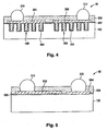
- the capacitance per unit area of capacitor 40 is significantly increased by the formation of trenches 406 under electrodes 304 and 306.
- Dielectric layer 402 extends into trenches 304 and 306 and lines the walls thereof in the manner of a normal trench-gated MOSFET.
- Trenches 304 and 306 are filled with a conductive material 404, such as polysilicon, which is in electrical contact with electrodes 304 and 306. The net result is to increase the effective area of the interface between the "plates" and the dielectric layer of the capacitor.
- Fig. 5 shows a cross-sectional view of a capacitor 50 which is similar to capacitor 30 shown in Fig. 3 except that the electrode 504 is in electrical contact with the N+ substrate 102. Electrode 502 is separated from substrate 102 by a dielectric layer 506 having a defined thickness. Capacitor 50 has a capacitance value per unit area similar to that of capacitor 10 shown in Fig. 1 . However, the lateral placement of electrodes 502 and 504 leads to a larger effective series resistance (ESR) which is a function of the lateral dimension of the device.
- ESR effective series resistance
- Fig. 6 is a top view of a capacitor 60 in which the first electrode 602 has fingers 602a-602c that are interdigitated with fingers 604a-604d of the second electrode 604.
- Fig. 7 is a cross-sectional view taken at cross-section 7-7 shown in Fig. 6 (note that the scales of Figs. 6 and 7 are not the same).
- a thin dielectric layer 618 is formed over the substrate.
- a relatively thick dielectric layer 614 separates the remaining "palm" portion of electrode 602 from N+ substrate 102, and a relatively thick dielectric layer 616 separates the palm portion of electrode 604 from substrate 102.
- capacitor 60 is determined by the number and dimensions of the fingers. As indicated in Fig. 6 , electrode 604 can be separated from the N+ substrate by a dielectric layer, creating a pair of capacitors, or it can be in direct electrical contact with the N + substrate (in the manner of electrode 504 in Fig. 5 ), creating a single capacitor. In many embodiments, the pitch "p" of the finger layout will be less than 300 ⁇ m.
- a capacitor 60 wherein electrode 604 is in direct electrical contact with the substrate and the pitch of the interdigitated fingers is 250 ⁇ m (finger width of 200 ⁇ m, spacing of 50 ⁇ m) and the thin dielectric layer 618 is a 0.1 ⁇ m-thick oxide layer, has a capacitance of 150 pF/mm 2 and an ESR of 12 m ⁇ mm 2 .
- ESDs electrostatic discharges
- D1, D2 electrostatic discharges
- One way to protect against ESDs is to connect a pair of oppositely-directed Zener diodes D1, D2 in parallel with the capacitor, as shown in the circuit diagram of Fig. 8 .
- D1, D2 When an ESD voltage spike occurs, one of the diodes conducts in the forward direction and the other diode breaks down at a predetermined voltage and conducts in the reverse direction, thereby providing a current path around the capacitor.
- the voltage at which current flows in the protective path is equal to the reverse breakdown voltage of one diode plus the voltage at which the other diode conducts in the forward direction (typically about 0.5 V).
- the term "oppositely-directed" means that the diodes are connected in series with either their anodes facing each other or their cathodes facing each other, such that any current in the series path flows through one of the diodes in the forward direction and through the other diode in the reverse direction.
- the protective diodes can be formed in the substrate itself, as shown in the ESD-protected capacitor arrangement of Fig. 9 .
- An N+ region 902, a P region 904 and an N+ region 906 are formed in substrate 102 beneath electrode 106.
- the regions are formed such that there is a first PN junction between N+ region 902 and P region 904 that represents one of the diodes and a second PN junction between P region 904 and N+ region 906 that represents the other diode.
- the doping concentrations of regions 902, 904 and 906 are set such that the PN junctions break down in the reverse direction at a desired voltage.
- the breakdown voltage depends on the doping concentration on the more lightly doped side of the PN junction and other factors that are well-known in the art. See, for example, Sze, Physics of Semiconductor Devices, 2nd Ed., John Wiley & Sons (1981), pp. 99-108 , which is incorporated herein by reference.
- the second N+ region 906 which extends into the P region 904 as well as the N+ substrate, is used to provide a symmetrical breakdown characteristic of the diode pair. In some embodiments, N+ region 906 may be omitted.
- the impedance of the Zener diodes can be set at a level that is higher than the capacitor by a factor of 1000 or more.
- Fig. 10a shows the IV characteristic of the structure with electrode 106 biased positive with respect to electrode 114 ("accumulation bias")
- Fig. 10b shows the IV characteristic of the structure with electrode 106 biased negative with respect to electrode 114 ("depletion bias”).
- the diode pair breaks down in the range of 16-19 V in either direction.
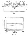
- Fig. 11 shows that the effective capacitance of the combined capacitor and ESD-structure remains quite constant at about 0.15 pF throughout the frequency range from 0.1 to 10 GHz.
Landscapes
- Semiconductor Integrated Circuits (AREA)
- Fixed Capacitors And Capacitor Manufacturing Machines (AREA)
- Internal Circuitry In Semiconductor Integrated Circuit Devices (AREA)
Claims (11)
- Structure de condensateur haute fréquence (30 ; 40 ; 60) comprenant :un substrat semi-conducteur fortement dopé (102) ayant des première et seconde surfaces principales ;une première partie de couche diélectrique (302 ; 402 ; 614, 618) formée sur la première surface principale du substrat (102) ;une première couche d'électrode (304 ; 602, 602c) formée sur la première partie de couche diélectrique (302 ; 402 ; 614, 618) et électriquement isolée du substrat (102) ;une seconde partie de couche diélectrique (302 ; 402 ; 616, 618) formée sur la première surface principale du substrat (102) ; etune seconde couche d'électrode (306 ; 604, 604c) formée sur la seconde partie de couche diélectrique (302 ; 402 ; 616, 618), la seconde couche d'électrode (306 ; 604, 604c) étant isolée électriquement du substrat (102) et de la première couche d'électrode (304 ; 602, 602c) ; dans laquelle les première (304 ; 602, 602c) et seconde (306 ; 604, 604c) couches d'électrode forment une paire de condensateurs connectés en série,caractérisée en ce que le substrat (102) représente la borne commune entre les condensateurs connectés en série.
- Structure de condensateur selon la revendication 1, dans laquelle la concentration de dopage du substrat semi-conducteur (102) est supérieure à 1 x 1019 cm-3.
- Structure de condensateur selon l'une quelconque des revendications précédentes, dans laquelle l'épaisseur des parties de couche diélectrique (302 ; 614, 616, 618) est supérieure ou égale à 0,005 micron.
- Structure de condensateur selon l'une quelconque des caractéristiques 1 à 3, comprenant une tranchée (406) dans le substrat (102) en dessous de la première partie de couche diélectrique (402), la première partie de couche diélectrique (402) s'étendant le long des parois de la tranchée (406), la tranchée contenant un matériau conducteur (404), le matériau conducteur étant en contact électrique avec la première électrode (304).
- Structure de condensateur selon la revendication 4, dans laquelle le matériau conducteur (404) comprend du polysilicium.
- Structure de condensateur selon l'une quelconque des revendications précédentes, dans laquelle les parties de couche diélectrique (302 ; 402) comprennent un oxyde.
- Dispositif condensateur selon la revendication 1, comprenant en outre :une couche de passivation (308, 608) recouvrant ladite première couche d'électrode (304 ; 602, 602c) et ladite seconde couche d'électrode (306 ; 604, 604c), une première ouverture étant formée dans ladite couche de passivation (308, 608) sur ladite première couche d'électrode (304 ; 602, 602c) et une seconde ouverture étant formée dans ladite couche de passivation (308, 608) sur ladite seconde couche d'électrode (306 ; 604, 604c).
- Dispositif condensateur selon la revendication 7, comprenant en outre :une première bille de métal (310 ; 610) dans ladite première ouverture, dans lequel ladite première bille de métal est électriquement couplée à ladite première couche d'électrode (304 ; 602, 602c) ; etune seconde bille de métal (312 ; 612) dans ladite seconde ouverture, dans lequel ladite seconde bille de métal est électriquement couplée à ladite seconde couche d'électrode (306 ; 604, 604c).
- Dispositif condensateur selon la revendication 1, dans lequel ladite première couche d'électrode (304 ; 602, 602c) comprend une première pluralité de doigts et ladite seconde couche d'électrode (306 ; 604, 604c) comprend une seconde pluralité de doigts, ladite première pluralité de doigts et ladite seconde pluralité de doigts étant interdigitées.
- Dispositif condensateur selon la revendication 9, dans lequel ladite première pluralité de doigts s'étend à partir d'une première partie commune de ladite première couche d'électrode (304 ; 602, 602c), ladite première couche diélectrique étant plus mince (618) sous ladite première pluralité de doigts que (614) sous ladite première partie commune.
- Dispositif condensateur selon la revendication 9, dans lequel ladite seconde pluralité de doigts s'étend d'une seconde partie commune de ladite seconde couche d'électrode (306 ; 604, 604c), ladite seconde couche diélectrique étant plus mince (618) sous ladite seconde pluralité de doigts que (616) sous ladite seconde partie commune.
Applications Claiming Priority (2)
| Application Number | Priority Date | Filing Date | Title |
|---|---|---|---|
| US09/661,483 US6538300B1 (en) | 2000-09-14 | 2000-09-14 | Precision high-frequency capacitor formed on semiconductor substrate |
| EP01307796A EP1189263B1 (fr) | 2000-09-14 | 2001-09-13 | Condensateur de précision à haute fréquence sur un substrat semiconducteur |
Related Parent Applications (2)
| Application Number | Title | Priority Date | Filing Date |
|---|---|---|---|
| EP01307796A Division EP1189263B1 (fr) | 2000-09-14 | 2001-09-13 | Condensateur de précision à haute fréquence sur un substrat semiconducteur |
| EP01307796.1 Division | 2001-09-13 |
Publications (2)
| Publication Number | Publication Date |
|---|---|
| EP1895569A1 EP1895569A1 (fr) | 2008-03-05 |
| EP1895569B1 true EP1895569B1 (fr) | 2013-06-12 |
Family
ID=24653791
Family Applications (3)
| Application Number | Title | Priority Date | Filing Date |
|---|---|---|---|
| EP07021795.5A Expired - Lifetime EP1895568B1 (fr) | 2000-09-14 | 2001-09-13 | Condensateur haute-fréquence formé sur un substrat semi-conducteur |
| EP01307796A Expired - Lifetime EP1189263B1 (fr) | 2000-09-14 | 2001-09-13 | Condensateur de précision à haute fréquence sur un substrat semiconducteur |
| EP07021796.3A Expired - Lifetime EP1895569B1 (fr) | 2000-09-14 | 2001-09-13 | Condensateur haute-fréquence de précision formé sur un substrat semi-conducteur |
Family Applications Before (2)
| Application Number | Title | Priority Date | Filing Date |
|---|---|---|---|
| EP07021795.5A Expired - Lifetime EP1895568B1 (fr) | 2000-09-14 | 2001-09-13 | Condensateur haute-fréquence formé sur un substrat semi-conducteur |
| EP01307796A Expired - Lifetime EP1189263B1 (fr) | 2000-09-14 | 2001-09-13 | Condensateur de précision à haute fréquence sur un substrat semiconducteur |
Country Status (7)
| Country | Link |
|---|---|
| US (3) | US6538300B1 (fr) |
| EP (3) | EP1895568B1 (fr) |
| JP (2) | JP3943879B2 (fr) |
| CN (1) | CN1182566C (fr) |
| DE (1) | DE60143510D1 (fr) |
| SG (1) | SG103315A1 (fr) |
| TW (1) | TW535251B (fr) |
Families Citing this family (47)
| Publication number | Priority date | Publication date | Assignee | Title |
|---|---|---|---|---|
| US6538300B1 (en) * | 2000-09-14 | 2003-03-25 | Vishay Intertechnology, Inc. | Precision high-frequency capacitor formed on semiconductor substrate |
| US7151036B1 (en) * | 2002-07-29 | 2006-12-19 | Vishay-Siliconix | Precision high-frequency capacitor formed on semiconductor substrate |
| US6605551B2 (en) * | 2000-12-08 | 2003-08-12 | Intel Corporation | Electrocoating process to form a dielectric layer in an organic substrate to reduce loop inductance |
| US20060246621A1 (en) * | 2002-02-14 | 2006-11-02 | Intel Corporation | Microelectronic die including thermally conductive structure in a substrate thereof and method of forming same |
| US20030151132A1 (en) * | 2002-02-14 | 2003-08-14 | Crippen Warren Stuart | Microelectronic die providing improved heat dissipation, and method of packaging same |
| US6934136B2 (en) * | 2002-04-24 | 2005-08-23 | Texas Instrument Incorporated | ESD protection of noise decoupling capacitors |
| US6815256B2 (en) * | 2002-12-23 | 2004-11-09 | Intel Corporation | Silicon building blocks in integrated circuit packaging |
| WO2004114397A1 (fr) * | 2003-06-20 | 2004-12-29 | Koninklijke Philips Electronics N.V. | Dispositif electronique, assemblage et procedes de fabrication d'un dispositif electronique |
| DE102004006484A1 (de) * | 2004-02-10 | 2005-08-25 | Infineon Technologies Ag | Integrierte Schaltungsanordnungen mit ESD-festem Kondensator und Herstellungsverfahren |
| US7253522B2 (en) * | 2004-06-02 | 2007-08-07 | Avx Israel, Ltd. | Integrated capacitor for RF applications with Ta adhesion layer |
| US7262139B2 (en) * | 2004-06-02 | 2007-08-28 | Avx Israel, Ltd. | Method suitable for batch ion etching of copper |
| US8154105B2 (en) * | 2005-09-22 | 2012-04-10 | International Rectifier Corporation | Flip chip semiconductor device and process of its manufacture |
| US7426102B2 (en) * | 2006-05-01 | 2008-09-16 | Vishay Intertechnology, Inc. | High precision capacitor with standoff |
| US20070267719A1 (en) * | 2006-05-18 | 2007-11-22 | Jin Shown Shie | Structure and manufacturing method of high precision chip capacitor fabricated on silicon substrate |
| US7589392B2 (en) * | 2006-06-16 | 2009-09-15 | Semiconductor Components Industries, L.L.C. | Filter having integrated floating capacitor and transient voltage suppression structure and method of manufacture |
| US7579670B2 (en) * | 2006-07-03 | 2009-08-25 | Semiconductor Components Industries, L.L.C. | Integrated filter having ground plane structure |
| JP5301108B2 (ja) * | 2007-04-20 | 2013-09-25 | セミコンダクター・コンポーネンツ・インダストリーズ・リミテッド・ライアビリティ・カンパニー | 半導体装置 |
| US8440916B2 (en) * | 2007-06-28 | 2013-05-14 | Intel Corporation | Method of forming a substrate core structure using microvia laser drilling and conductive layer pre-patterning and substrate core structure formed according to the method |
| JP5298559B2 (ja) * | 2007-06-29 | 2013-09-25 | 富士通株式会社 | 半導体装置及びその製造方法 |
| US8492872B2 (en) * | 2007-10-05 | 2013-07-23 | Taiwan Semiconductor Manufacturing Co., Ltd. | On-chip inductors with through-silicon-via fence for Q improvement |
| US20090095338A1 (en) * | 2007-10-11 | 2009-04-16 | James Chyl Lai | Solar power source |
| US9590027B2 (en) * | 2009-04-20 | 2017-03-07 | Nxp B.V. | Method for fabricating an integrated-passives device with a MIM capacitor and a high-accuracy resistor on top |
| JP5234521B2 (ja) * | 2009-08-21 | 2013-07-10 | Tdk株式会社 | 電子部品及びその製造方法 |
| DE102009038709B4 (de) * | 2009-08-25 | 2017-05-11 | Infineon Technologies Austria Ag | Halbleiterbauelement mit dielektrischem Schichtstapel |
| WO2014069363A1 (fr) | 2012-11-02 | 2014-05-08 | ローム株式会社 | Condensateur en chip, ensemble circuit et dispositif électronique |
| US9860985B1 (en) | 2012-12-17 | 2018-01-02 | Lockheed Martin Corporation | System and method for improving isolation in high-density laminated printed circuit boards |
| CN105051887B (zh) | 2013-02-28 | 2018-04-17 | 株式会社村田制作所 | 半导体装置 |
| WO2014132937A1 (fr) | 2013-02-28 | 2014-09-04 | 株式会社村田製作所 | Dispositif de protection contre les décharges électrostatiques (esd) |
| CN205508776U (zh) | 2013-02-28 | 2016-08-24 | 株式会社村田制作所 | 半导体装置 |
| JP5843049B2 (ja) | 2013-04-05 | 2016-01-13 | 株式会社村田製作所 | Esd保護デバイス |
| WO2014181565A1 (fr) * | 2013-05-07 | 2014-11-13 | 株式会社村田製作所 | Dispositif à semi-conducteur et dispositif de protection esd |
| JP5575309B1 (ja) * | 2013-08-05 | 2014-08-20 | 有限会社 ナプラ | 集積回路装置 |
| KR101677738B1 (ko) * | 2014-07-02 | 2016-11-21 | 조인셋 주식회사 | Esd 내성을 가지는 폴리머 커패시터 |
| US10217810B2 (en) * | 2015-12-07 | 2019-02-26 | Microchip Technology Incorporated | Capacitor formed on heavily doped substrate |
| WO2018034067A1 (fr) * | 2016-08-19 | 2018-02-22 | 株式会社村田製作所 | Dispositif à semi-conducteur avec condensateur |
| US10056461B2 (en) | 2016-09-30 | 2018-08-21 | Alpha And Omega Semiconductor Incorporated | Composite masking self-aligned trench MOSFET |
| US10199492B2 (en) | 2016-11-30 | 2019-02-05 | Alpha And Omega Semiconductor Incorporated | Folded channel trench MOSFET |
| WO2019138803A1 (fr) * | 2018-01-10 | 2019-07-18 | 株式会社村田製作所 | Condensateur et circuit limiteur |
| KR102068806B1 (ko) * | 2018-01-31 | 2020-01-22 | 삼성전기주식회사 | 커패시터 및 그 제조방법 |
| US11674916B2 (en) * | 2018-11-12 | 2023-06-13 | Sciosense B.V. | Gas sensor |
| US11715594B2 (en) * | 2021-05-27 | 2023-08-01 | International Business Machines Corporation | Vertically-stacked interdigitated metal-insulator-metal capacitor for sub-20 nm pitch |
| JP2023049960A (ja) * | 2021-09-29 | 2023-04-10 | ローム株式会社 | チップ部品 |
| JP7817807B2 (ja) * | 2021-09-29 | 2026-02-19 | ローム株式会社 | チップ部品 |
| JP2023049961A (ja) * | 2021-09-29 | 2023-04-10 | ローム株式会社 | チップ部品 |
| CN114038805A (zh) * | 2021-11-24 | 2022-02-11 | 苏州科阳半导体有限公司 | 一种半导体芯片的封装结构及封装方法 |
| CN114551438B (zh) * | 2022-02-24 | 2026-04-14 | 武汉华星光电半导体显示技术有限公司 | 显示面板 |
| CN118841409B (zh) * | 2024-09-20 | 2025-02-07 | 苏州凌存科技有限公司 | 一种半导体电容、阵列及其制备方法 |
Citations (8)
| Publication number | Priority date | Publication date | Assignee | Title |
|---|---|---|---|---|
| JPS61263251A (ja) * | 1985-05-17 | 1986-11-21 | Nec Corp | 半導体装置 |
| US4751562A (en) * | 1982-06-30 | 1988-06-14 | Fujitsu Limited | Field-effect semiconductor device |
| JPS63239939A (ja) * | 1987-03-27 | 1988-10-05 | Toshiba Corp | 半導体基体内への不純物導入方法及び装置 |
| US4937660A (en) * | 1988-12-21 | 1990-06-26 | At&T Bell Laboratories | Silicon-based mounting structure for semiconductor optical devices |
| JPH02270311A (ja) * | 1989-04-11 | 1990-11-05 | Mitsui Petrochem Ind Ltd | 薄膜コンデンサ |
| JPH10336022A (ja) * | 1997-06-03 | 1998-12-18 | Hitachi Ltd | 差動チャージポンプ回路 |
| JPH10335368A (ja) * | 1997-05-30 | 1998-12-18 | Sanyo Electric Co Ltd | ワイヤボンディング構造及び半導体装置 |
| US6538300B1 (en) * | 2000-09-14 | 2003-03-25 | Vishay Intertechnology, Inc. | Precision high-frequency capacitor formed on semiconductor substrate |
Family Cites Families (24)
| Publication number | Priority date | Publication date | Assignee | Title |
|---|---|---|---|---|
| US3471756A (en) * | 1968-03-11 | 1969-10-07 | Us Army | Metal oxide-silicon diode containing coating of vanadium pentoxide-v2o5 deposited on n-type material with nickel electrodes |
| US4246502A (en) * | 1978-08-16 | 1981-01-20 | Mitel Corporation | Means for coupling incompatible signals to an integrated circuit and for deriving operating supply therefrom |
| GB2060253A (en) * | 1979-10-01 | 1981-04-29 | Trw Inc | MIS Capacitors |
| US4432035A (en) * | 1982-06-11 | 1984-02-14 | International Business Machines Corp. | Method of making high dielectric constant insulators and capacitors using same |
| JP2736061B2 (ja) * | 1987-09-17 | 1998-04-02 | 株式会社東芝 | 半導体装置の製造方法 |
| EP0412514A1 (fr) * | 1989-08-08 | 1991-02-13 | Nec Corporation | Dispositif capacitif |
| JP2740038B2 (ja) * | 1990-06-18 | 1998-04-15 | 株式会社東芝 | Mos(mis)型コンデンサー |
| US5202279A (en) * | 1990-12-05 | 1993-04-13 | Texas Instruments Incorporated | Poly sidewall process to reduce gated diode leakage |
| US5208726A (en) * | 1992-04-03 | 1993-05-04 | Teledyne Monolithic Microwave | Metal-insulator-metal (MIM) capacitor-around-via structure for a monolithic microwave integrated circuit (MMIC) and method of manufacturing same |
| JP2884917B2 (ja) * | 1992-06-08 | 1999-04-19 | 日本電気株式会社 | 薄膜キャパシタおよび集積回路 |
| US5414284A (en) * | 1994-01-19 | 1995-05-09 | Baxter; Ronald D. | ESD Protection of ISFET sensors |
| US5841182A (en) * | 1994-10-19 | 1998-11-24 | Harris Corporation | Capacitor structure in a bonded wafer and method of fabrication |
| GB2297602B (en) * | 1995-02-03 | 1999-03-24 | Luk Lamellen & Kupplungsbau | Torsional vibration damper |
| JPH08236698A (ja) * | 1995-02-27 | 1996-09-13 | Nec Eng Ltd | 半導体装置 |
| JPH0964275A (ja) * | 1995-08-23 | 1997-03-07 | Mitsubishi Electric Corp | 高周波集積回路装置 |
| US5706163A (en) * | 1995-11-28 | 1998-01-06 | California Micro Devices Corporation | ESD-protected thin film capacitor structures |
| US5627094A (en) * | 1995-12-04 | 1997-05-06 | Chartered Semiconductor Manufacturing Pte, Ltd. | Stacked container capacitor using chemical mechanical polishing |
| US5889299A (en) * | 1996-02-22 | 1999-03-30 | Kabushiki Kaisha Toshiba | Thin film capacitor |
| KR100207466B1 (ko) * | 1996-02-28 | 1999-07-15 | 윤종용 | 반도체 장치의 커패시터 제조방법 |
| JP2795259B2 (ja) * | 1996-04-17 | 1998-09-10 | 日本電気株式会社 | 半導体装置およびその製造方法 |
| US5811868A (en) * | 1996-12-20 | 1998-09-22 | International Business Machines Corp. | Integrated high-performance decoupling capacitor |
| JP3900542B2 (ja) * | 1997-03-24 | 2007-04-04 | セイコーエプソン株式会社 | 半導体容量装置及びそれを用いた半導体装置 |
| KR100292689B1 (ko) * | 1998-06-03 | 2001-07-12 | 김영환 | 캐패시터및그형성방법 |
| JP2000150810A (ja) * | 1998-11-17 | 2000-05-30 | Toshiba Microelectronics Corp | 半導体装置及びその製造方法 |
-
2000
- 2000-09-14 US US09/661,483 patent/US6538300B1/en not_active Expired - Lifetime
-
2001
- 2001-09-10 TW TW090122394A patent/TW535251B/zh active
- 2001-09-13 EP EP07021795.5A patent/EP1895568B1/fr not_active Expired - Lifetime
- 2001-09-13 EP EP01307796A patent/EP1189263B1/fr not_active Expired - Lifetime
- 2001-09-13 DE DE60143510T patent/DE60143510D1/de not_active Expired - Lifetime
- 2001-09-13 EP EP07021796.3A patent/EP1895569B1/fr not_active Expired - Lifetime
- 2001-09-13 SG SG200105622A patent/SG103315A1/en unknown
- 2001-09-14 JP JP2001279888A patent/JP3943879B2/ja not_active Expired - Fee Related
- 2001-09-14 CN CNB011355794A patent/CN1182566C/zh not_active Expired - Fee Related
-
2002
- 2002-07-29 US US10/208,599 patent/US6621143B2/en not_active Expired - Lifetime
- 2002-07-29 US US10/208,121 patent/US6621142B2/en not_active Expired - Lifetime
-
2006
- 2006-09-21 JP JP2006255468A patent/JP5016284B2/ja not_active Expired - Fee Related
Patent Citations (8)
| Publication number | Priority date | Publication date | Assignee | Title |
|---|---|---|---|---|
| US4751562A (en) * | 1982-06-30 | 1988-06-14 | Fujitsu Limited | Field-effect semiconductor device |
| JPS61263251A (ja) * | 1985-05-17 | 1986-11-21 | Nec Corp | 半導体装置 |
| JPS63239939A (ja) * | 1987-03-27 | 1988-10-05 | Toshiba Corp | 半導体基体内への不純物導入方法及び装置 |
| US4937660A (en) * | 1988-12-21 | 1990-06-26 | At&T Bell Laboratories | Silicon-based mounting structure for semiconductor optical devices |
| JPH02270311A (ja) * | 1989-04-11 | 1990-11-05 | Mitsui Petrochem Ind Ltd | 薄膜コンデンサ |
| JPH10335368A (ja) * | 1997-05-30 | 1998-12-18 | Sanyo Electric Co Ltd | ワイヤボンディング構造及び半導体装置 |
| JPH10336022A (ja) * | 1997-06-03 | 1998-12-18 | Hitachi Ltd | 差動チャージポンプ回路 |
| US6538300B1 (en) * | 2000-09-14 | 2003-03-25 | Vishay Intertechnology, Inc. | Precision high-frequency capacitor formed on semiconductor substrate |
Also Published As
| Publication number | Publication date |
|---|---|
| EP1189263A2 (fr) | 2002-03-20 |
| SG103315A1 (en) | 2004-04-29 |
| DE60143510D1 (de) | 2011-01-05 |
| JP2007005828A (ja) | 2007-01-11 |
| EP1895568B1 (fr) | 2014-07-16 |
| US6538300B1 (en) | 2003-03-25 |
| EP1189263B1 (fr) | 2010-11-24 |
| EP1189263A3 (fr) | 2005-04-27 |
| US20030057517A1 (en) | 2003-03-27 |
| JP3943879B2 (ja) | 2007-07-11 |
| JP2002176106A (ja) | 2002-06-21 |
| CN1346138A (zh) | 2002-04-24 |
| EP1895569A1 (fr) | 2008-03-05 |
| US6621142B2 (en) | 2003-09-16 |
| US6621143B2 (en) | 2003-09-16 |
| EP1895568A1 (fr) | 2008-03-05 |
| CN1182566C (zh) | 2004-12-29 |
| TW535251B (en) | 2003-06-01 |
| US20030030125A1 (en) | 2003-02-13 |
| JP5016284B2 (ja) | 2012-09-05 |
Similar Documents
| Publication | Publication Date | Title |
|---|---|---|
| EP1895568B1 (fr) | Condensateur haute-fréquence formé sur un substrat semi-conducteur | |
| US9136060B2 (en) | Precision high-frequency capacitor formed on semiconductor substrate | |
| US6844241B2 (en) | Fabrication of semiconductor structures having multiple conductive layers in an opening | |
| US5952695A (en) | Silicon-on-insulator and CMOS-on-SOI double film structures | |
| KR100243658B1 (ko) | 기판 변환기술을 이용한 인덕터 소자 및 그 제조 방법 | |
| US5304506A (en) | On chip decoupling capacitor | |
| EP1351304B1 (fr) | Condensateurs pour circuits intégrés | |
| KR101264926B1 (ko) | 반도체 장치의 제조 방법 및 반도체 장치 | |
| EP2827373A2 (fr) | Dispositif de protection et procédés de fabrication associés | |
| US6262442B1 (en) | Zener diode and RC network combination semiconductor device for use in integrated circuits | |
| JPH06151846A (ja) | 半導体装置 | |
| US11978808B2 (en) | Vertical etch heterolithic integrated circuit devices | |
| US20090085150A1 (en) | Semiconductor device having silicon-on-insulator (SOI) structure and method of forming semiconductor device | |
| JP2000012778A (ja) | 半導体集積回路の入力保護回路装置 |
Legal Events
| Date | Code | Title | Description |
|---|---|---|---|
| PUAI | Public reference made under article 153(3) epc to a published international application that has entered the european phase |
Free format text: ORIGINAL CODE: 0009012 |
|
| 17P | Request for examination filed |
Effective date: 20071204 |
|
| AC | Divisional application: reference to earlier application |
Ref document number: 1189263 Country of ref document: EP Kind code of ref document: P |
|
| AK | Designated contracting states |
Kind code of ref document: A1 Designated state(s): DE FR GB |
|
| AKX | Designation fees paid |
Designated state(s): DE FR GB |
|
| 17Q | First examination report despatched |
Effective date: 20081021 |
|
| GRAP | Despatch of communication of intention to grant a patent |
Free format text: ORIGINAL CODE: EPIDOSNIGR1 |
|
| GRAS | Grant fee paid |
Free format text: ORIGINAL CODE: EPIDOSNIGR3 |
|
| GRAA | (expected) grant |
Free format text: ORIGINAL CODE: 0009210 |
|
| AC | Divisional application: reference to earlier application |
Ref document number: 1189263 Country of ref document: EP Kind code of ref document: P |
|
| AK | Designated contracting states |
Kind code of ref document: B1 Designated state(s): DE FR GB |
|
| REG | Reference to a national code |
Ref country code: GB Ref legal event code: FG4D |
|
| REG | Reference to a national code |
Ref country code: DE Ref legal event code: R096 Ref document number: 60148077 Country of ref document: DE Effective date: 20130808 |
|
| PLBE | No opposition filed within time limit |
Free format text: ORIGINAL CODE: 0009261 |
|
| STAA | Information on the status of an ep patent application or granted ep patent |
Free format text: STATUS: NO OPPOSITION FILED WITHIN TIME LIMIT |
|
| 26N | No opposition filed |
Effective date: 20140313 |
|
| REG | Reference to a national code |
Ref country code: DE Ref legal event code: R097 Ref document number: 60148077 Country of ref document: DE Effective date: 20140313 |
|
| PGFP | Annual fee paid to national office [announced via postgrant information from national office to epo] |
Ref country code: FR Payment date: 20140917 Year of fee payment: 14 Ref country code: GB Payment date: 20140929 Year of fee payment: 14 |
|
| PGFP | Annual fee paid to national office [announced via postgrant information from national office to epo] |
Ref country code: DE Payment date: 20140929 Year of fee payment: 14 |
|
| REG | Reference to a national code |
Ref country code: DE Ref legal event code: R119 Ref document number: 60148077 Country of ref document: DE |
|
| GBPC | Gb: european patent ceased through non-payment of renewal fee |
Effective date: 20150913 |
|
| REG | Reference to a national code |
Ref country code: FR Ref legal event code: ST Effective date: 20160531 |
|
| PG25 | Lapsed in a contracting state [announced via postgrant information from national office to epo] |
Ref country code: GB Free format text: LAPSE BECAUSE OF NON-PAYMENT OF DUE FEES Effective date: 20150913 Ref country code: DE Free format text: LAPSE BECAUSE OF NON-PAYMENT OF DUE FEES Effective date: 20160401 |
|
| PG25 | Lapsed in a contracting state [announced via postgrant information from national office to epo] |
Ref country code: FR Free format text: LAPSE BECAUSE OF NON-PAYMENT OF DUE FEES Effective date: 20150930 |