EP1895829A2 - Dispositif de blindage pour protection électromagnétique - Google Patents
Dispositif de blindage pour protection électromagnétique Download PDFInfo
- Publication number
- EP1895829A2 EP1895829A2 EP07102253A EP07102253A EP1895829A2 EP 1895829 A2 EP1895829 A2 EP 1895829A2 EP 07102253 A EP07102253 A EP 07102253A EP 07102253 A EP07102253 A EP 07102253A EP 1895829 A2 EP1895829 A2 EP 1895829A2
- Authority
- EP
- European Patent Office
- Prior art keywords
- shielding
- cover
- emi
- disposed
- shielding cover
- Prior art date
- Legal status (The legal status is an assumption and is not a legal conclusion. Google has not performed a legal analysis and makes no representation as to the accuracy of the status listed.)
- Withdrawn
Links
Images





Classifications
-
- H—ELECTRICITY
- H05—ELECTRIC TECHNIQUES NOT OTHERWISE PROVIDED FOR
- H05K—PRINTED CIRCUITS; CASINGS OR CONSTRUCTIONAL DETAILS OF ELECTRIC APPARATUS; MANUFACTURE OF ASSEMBLAGES OF ELECTRICAL COMPONENTS
- H05K9/00—Screening of apparatus or components against electric or magnetic fields
- H05K9/0007—Casings
- H05K9/002—Casings with localised screening
- H05K9/0022—Casings with localised screening of components mounted on printed circuit boards [PCB]
- H05K9/0024—Shield cases mounted on a PCB, e.g. cans or caps or conformal shields
- H05K9/0026—Shield cases mounted on a PCB, e.g. cans or caps or conformal shields integrally formed from metal sheet
-
- H—ELECTRICITY
- H05—ELECTRIC TECHNIQUES NOT OTHERWISE PROVIDED FOR
- H05K—PRINTED CIRCUITS; CASINGS OR CONSTRUCTIONAL DETAILS OF ELECTRIC APPARATUS; MANUFACTURE OF ASSEMBLAGES OF ELECTRICAL COMPONENTS
- H05K9/00—Screening of apparatus or components against electric or magnetic fields
- H05K9/0007—Casings
- H05K9/002—Casings with localised screening
- H05K9/0022—Casings with localised screening of components mounted on printed circuit boards [PCB]
- H05K9/0037—Housings with compartments containing a PCB, e.g. partitioning walls
Definitions
- the present invention relates to a shielding device, and more particularly to a shielding device is adapted to cover electronic components, such as chips, CPU, and etc. for EMI shielding.
- a conventional shielding cover is provided to prevent the electromagnetic interference with the operation of the electronic elements as chip, CPU, etc. and the shielding cover is covered on an outer of electronic component installed on a circuit board so as to provide EMI shielding effect.
- the above-mentioned shielding cover has to be welded on the circuit board by using SMT processing. Hence, adapted materials for the shielding cover are limited and more expensive. Further, if the electronic component needs to be maintained, an upper cover of the shielding cover has to be lifted upwardly and be away from the shielding cover to add extra back-shielding upper cover so as to increase costs.
- the inventor of the present invention recognizes the above shortage should be corrected and special effort has been paid to research this field.
- the present invention is presented with reasonable design and good effect to resolve the above problems.
- the shielding device for EMI shielding is disposed on a housing of an electronic device with an electronic component disposed on a circuit board, comprises a shielding cover is connected on the housing; an elastic unit is disposed on the shielding cover; and the shielding cover covered on an outside of the electronic component.
- the present invention has the following advantages:
- the present invention provides a shielding device for EMI shielding is disposed on a housing 1 of an electronic device and comprises a shielding cover 2 and an elastic unit 3, wherein the housing 1 is used to fix the shielding cover 2.
- the housing 1 has a plurality of connecting elements 11 thereon and the connecting elements 11 can be integrally formed with the housing 1, or formed on the housing 1 by using a combining method.
- the connecting elements 11 are made of fusible material.
- the shielding cover 2 is a metal element and is a squared-shaped or other-shaped hollow object and has a top plate 21 and four side plates 22 extended downwardly from edges of the top plate 21, and a containing space 23 is formed between the top plate 21 and the side plates 22.
- the containing space 23 is disposed in the shielding cover 2 to contain an electronic component 4 fixed on a circuit board 5 of the electronic device so that the shielding cover 2 can be covered on an outside of the electronic component 4.
- a lug 24 is formed from each of the four corners of the top plate 21, each of the lugs 24 has a connecting hole 25 thereon so that the connecting elements 11 can be inserted into the corresponding connecting holes 25 and fixed to the connecting holes 25 by using a heat-melting way so that the shielding cover 2 can be connected to a position corresponded to the electronic component 4 on the housing 1.
- the shielding cover 2 can be connected not only by using a heat-melting way on the housing 1 but also by using a rivet-jointing, spot-welding, fastening-jointing, or spiral-jointing way.
- a plurality of bumps 34 are formed on the top plate 21 of the shielding cover 2 by using a punching way, and the elastic unit 3 is composed of the bumps 34.
- the bumps 34 are protruded on a top surface of the top plate 21 to press a bottom surface of the housing 1 so as to provide a pressed downwardly force to the shielding cover 2 to contact rigidly a bottom edge of the shielding cover 2 and a top surface of the circuit board 5.
- the shielding cover 2 is covered on an outside of the electronic component 4 to provide an EMI shielding effect so that the electronic component 4 can't be influenced by the EMI.
- the electronic component 4 needs to be maintained only if separating the housing 1 and the circuit board 5 so as to apart the electronic component 4 from the shielding cover 2. On the other hand, it is easily to cover the shielding cover 2 on the outside of the electronic component 4 as long as to assemble the housing 1 and the circuit board 5.
- the elastic unit 3 is integrally formed with a bottom edge of the side plate 22 of the shielding cover 2 or disposed on the bottom edge of the side plate 22 by using an assembly way, and in that the elastic unit 3 is a colloid 31.
- the shielding cover 2 is covered on the outside of the electronic component 4 by dispensing to assemble the colloid 31 on the bottom edge of the side plate 22 to contact rigidly the shielding cover 2 and the circuit board 5 so that the electronic component 4 can't be influenced by the EMI.
- the electronic component 4 needs to be maintained only if separating the housing 1, the circuit board 5, and the elastic unit 3 so as to apart the electronic component 4 from the shielding cover 2. On the other hand, it is easily to cover the shielding cover 2 on the outside of the electronic component 4 as long as to assemble the housing 1 and the circuit board 5.
- the connecting holes 25 are disposed directly on the top plate 21 of the shielding cover 2.
- the connecting element 11 is connected with the connecting holes 25 by using a heat-melting way so that the shielding cover 2 can be connected to a position corresponded to the electronic component 4 on the housing 1.
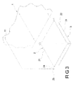
- the elastic unit 3 are some elastic pieces 32, 33 integrally formed with the bottom edge of the side plate 22 of the shielding cover 2 and the elastic pieces 32 can be curve extended outwardly (shown in Fig. 5 and Fig. 6) or curved extended inwardly (shown in Fig. 7 and Fig. 8).
- the shielding cover 2 is covered on an outside of the electronic component 4, and the elastic pieces 32, 33 are pressed the top surface of the circuit board 5 so that the elastic pieces 32, 33 are disposed between the side plate 22 of the shielding cover 2 and the circuit board 5 to contact rigidly the shielding cover 2 and the circuit board 5.
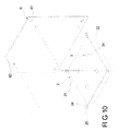
- the electronic device has a middle board 6 therein, and the shielding cover 2 is disposed on the middle board 6.
- the middle board 6 is a plate made of metal, plastic, or other materials, and the middle board 6 is also called as an inner board without having a limited shape.
- An edge of the middle board 6 has a plurality of fixed holes 61 to make the middle board 6 be firmly locked in the electronic device by the screws.
- the middle board 6 is firmed fixed on the circuit board 5 or the housing 1, however, the fixed way is not limited.
- the middle board 6 can be fixed on the circuit board 5 or the housing 1 of the electronic device by using a method of heat-melting, rivet-jointing, spot-welding, fastening-jointing, or spiral-jointing.
- the middle board 6 has a plurality of connecting elements 62 thereon and the connecting elements 62 can be integrally formed with the middle board 6, or formed on the middle board 6 by using a combining method.
- the connecting elements 62 are made of fusible material, and the connecting elements 62 can be inserted into the corresponding connecting holes 25 and fixed to the connecting holes 25 by using a heat-melting way so that the shielding cover 2 can be connected to a position corresponded to the electronic component 4 on the middle board 6.
- the shielding cover 2 can be connected not only by using a heat-melting way on the middle board 6 but also by using a rivet-jointing, spot-welding, fastening-jointing, or spiral-jointing way.
- a plurality of bumps 34 are formed on the top plate 21 of the shielding cover 2 by using a punching way, and the elastic unit 3 is composed of the bumps 34.
- the bumps 34 are protruded on a top surface of the top plate 21 to press a bottom surface of the middle board 6 so as to provide a pressed downwardly force to the shielding cover 2 to contact rigidly a bottom edge of the shielding cover 2 and a top surface of the circuit board 5.
- the shielding cover 2 is covered on an outside of the electronic component 4 to provide an EMI shielding effect so that the electronic component 4 can't be influenced by the EMI.
- the shielding cover 2 doesn't be welded on the circuit board 5 by using SMT processing, the shielding cover 2 is adapted in various materials to reduce substantially material costs. Further, if the electronic component 4 needs to be maintained only if separating the housing 1 and the circuit board 5, or opening the housing 1 to separate the housing 1, the middle board 6 and the circuit board 5 so as to apart the electronic component 4 from the shielding cover 2, and it is easily to cover the shielding cover 2 on the outside of the electronic component 4 as long as to assemble the housing 1 and the circuit board 5 or fix the middle board 6 in the electronic device without installing extra back-shielding upper cover.
Landscapes
- Engineering & Computer Science (AREA)
- Microelectronics & Electronic Packaging (AREA)
- Shielding Devices Or Components To Electric Or Magnetic Fields (AREA)
Applications Claiming Priority (1)
| Application Number | Priority Date | Filing Date | Title |
|---|---|---|---|
| CNU2006201330546U CN200947722Y (zh) | 2006-08-29 | 2006-08-29 | 防电磁干扰的遮蔽装置 |
Publications (2)
| Publication Number | Publication Date |
|---|---|
| EP1895829A2 true EP1895829A2 (fr) | 2008-03-05 |
| EP1895829A3 EP1895829A3 (fr) | 2010-04-14 |
Family
ID=38734781
Family Applications (1)
| Application Number | Title | Priority Date | Filing Date |
|---|---|---|---|
| EP07102253A Withdrawn EP1895829A3 (fr) | 2006-08-29 | 2007-02-13 | Dispositif de blindage pour protection électromagnétique |
Country Status (2)
| Country | Link |
|---|---|
| EP (1) | EP1895829A3 (fr) |
| CN (1) | CN200947722Y (fr) |
Cited By (1)
| Publication number | Priority date | Publication date | Assignee | Title |
|---|---|---|---|---|
| CN105101763A (zh) * | 2014-05-09 | 2015-11-25 | 国基电子(上海)有限公司 | 屏蔽罩 |
Families Citing this family (4)
| Publication number | Priority date | Publication date | Assignee | Title |
|---|---|---|---|---|
| CN102522387A (zh) * | 2011-12-21 | 2012-06-27 | 铜陵浩岩节能科技有限公司 | 一种表面贴装元器件静电保护器 |
| TWI773099B (zh) | 2021-01-25 | 2022-08-01 | 群光電能科技股份有限公司 | 殼體結構及具有殼體結構的電子裝置 |
| CN113556864B (zh) * | 2021-08-17 | 2025-03-25 | 京东方科技集团股份有限公司 | 一种柔性电路板结构及其制造方法、显示装置 |
| CN116828698B (zh) * | 2023-08-31 | 2023-12-15 | 深圳市卓汉材料技术有限公司 | 电磁屏蔽膜、电磁屏蔽封装体及其制备方法 |
Family Cites Families (3)
| Publication number | Priority date | Publication date | Assignee | Title |
|---|---|---|---|---|
| US5045635A (en) * | 1989-06-16 | 1991-09-03 | Schlegel Corporation | Conductive gasket with flame and abrasion resistant conductive coating |
| FR2798553B1 (fr) * | 1999-09-14 | 2001-10-12 | Sagem | Dispositif de protection de composants electroniques |
| JP4299152B2 (ja) * | 2004-01-08 | 2009-07-22 | 日本碍子株式会社 | 電磁波シールドケースおよびその製造方法 |
-
2006
- 2006-08-29 CN CNU2006201330546U patent/CN200947722Y/zh not_active Expired - Fee Related
-
2007
- 2007-02-13 EP EP07102253A patent/EP1895829A3/fr not_active Withdrawn
Non-Patent Citations (1)
| Title |
|---|
| None |
Cited By (1)
| Publication number | Priority date | Publication date | Assignee | Title |
|---|---|---|---|---|
| CN105101763A (zh) * | 2014-05-09 | 2015-11-25 | 国基电子(上海)有限公司 | 屏蔽罩 |
Also Published As
| Publication number | Publication date |
|---|---|
| EP1895829A3 (fr) | 2010-04-14 |
| CN200947722Y (zh) | 2007-09-12 |
Similar Documents
| Publication | Publication Date | Title |
|---|---|---|
| US6377472B1 (en) | Shielding device | |
| US7985090B2 (en) | Socket with an improved cover lid | |
| US7435139B2 (en) | Electrical connector having improved shield | |
| US6191950B1 (en) | Snap-together printed circuit card cover with integral card support | |
| EP2290685A1 (fr) | Substrat d'emballage | |
| US7442881B1 (en) | Shielding device | |
| EP1895829A2 (fr) | Dispositif de blindage pour protection électromagnétique | |
| US20070238357A1 (en) | Electrical connector | |
| US20090268420A1 (en) | Shielding assembly | |
| US20050205285A1 (en) | Lift-type positioning structure for bracket of computer interface card | |
| JP3959529B2 (ja) | 電子部品取付用ソケット | |
| US5463531A (en) | PCMCIA electronics housing | |
| US7452234B2 (en) | Socket connector with matchable padding | |
| US6469912B1 (en) | Electrical apparatus having a cover member adapted to provide electromagnetic interference shielding to an electronic component | |
| CN101355867B (zh) | 屏蔽装置 | |
| US7867004B2 (en) | Electrical connector with improved stiffener device | |
| US7880096B2 (en) | Shielding device with a replaceable top | |
| JP4890400B2 (ja) | 電子回路モジュール | |
| US20080025011A1 (en) | Shielding device for EMI shielding | |
| JP2000340305A (ja) | 外部インターフェースコネクタの接地構造 | |
| US7473106B2 (en) | IC socket connector configured by discrete wafers assembled to a frame | |
| EP2129206A2 (fr) | Unité à haute fréquence | |
| US20050243532A1 (en) | Packaging structure of electronic card | |
| CN212303258U (zh) | 一种热敏电阻 | |
| EP1003215A2 (fr) | Dissipateur de chaleur avec bride intégrale auto-bloquante |
Legal Events
| Date | Code | Title | Description |
|---|---|---|---|
| PUAI | Public reference made under article 153(3) epc to a published international application that has entered the european phase |
Free format text: ORIGINAL CODE: 0009012 |
|
| 17P | Request for examination filed |
Effective date: 20070213 |
|
| AK | Designated contracting states |
Kind code of ref document: A2 Designated state(s): AT BE BG CH CY CZ DE DK EE ES FI FR GB GR HU IE IS IT LI LT LU LV MC NL PL PT RO SE SI SK TR |
|
| AX | Request for extension of the european patent |
Extension state: AL BA HR MK YU |
|
| PUAL | Search report despatched |
Free format text: ORIGINAL CODE: 0009013 |
|
| AK | Designated contracting states |
Kind code of ref document: A3 Designated state(s): AT BE BG CH CY CZ DE DK EE ES FI FR GB GR HU IE IS IT LI LT LU LV MC NL PL PT RO SE SI SK TR |
|
| AX | Request for extension of the european patent |
Extension state: AL BA HR MK RS |
|
| 17Q | First examination report despatched |
Effective date: 20100525 |
|
| AKX | Designation fees paid |
Designated state(s): AT BE BG CH CY CZ DE DK EE ES FI FR GB GR HU IE IS IT LI LT LU LV MC NL PL PT RO SE SI SK TR |
|
| STAA | Information on the status of an ep patent application or granted ep patent |
Free format text: STATUS: THE APPLICATION IS DEEMED TO BE WITHDRAWN |
|
| 18D | Application deemed to be withdrawn |
Effective date: 20120901 |