EP1897965B1 - Verfahren zum Beseitigen von Ausscheidungen aus einem II-VI Halbleitermaterial durch Glühen. - Google Patents
Verfahren zum Beseitigen von Ausscheidungen aus einem II-VI Halbleitermaterial durch Glühen. Download PDFInfo
- Publication number
- EP1897965B1 EP1897965B1 EP07115691A EP07115691A EP1897965B1 EP 1897965 B1 EP1897965 B1 EP 1897965B1 EP 07115691 A EP07115691 A EP 07115691A EP 07115691 A EP07115691 A EP 07115691A EP 1897965 B1 EP1897965 B1 EP 1897965B1
- Authority
- EP
- European Patent Office
- Prior art keywords
- temperature
- precipitates
- semiconductor material
- solid
- annealing
- Prior art date
- Legal status (The legal status is an assumption and is not a legal conclusion. Google has not performed a legal analysis and makes no representation as to the accuracy of the status listed.)
- Active
Links
Images


Classifications
-
- C—CHEMISTRY; METALLURGY
- C22—METALLURGY; FERROUS OR NON-FERROUS ALLOYS; TREATMENT OF ALLOYS OR NON-FERROUS METALS
- C22F—CHANGING THE PHYSICAL STRUCTURE OF NON-FERROUS METALS AND NON-FERROUS ALLOYS
- C22F1/00—Changing the physical structure of non-ferrous metals or alloys by heat treatment or by hot or cold working
- C22F1/16—Changing the physical structure of non-ferrous metals or alloys by heat treatment or by hot or cold working of other metals or alloys based thereon
-
- C—CHEMISTRY; METALLURGY
- C30—CRYSTAL GROWTH
- C30B—SINGLE-CRYSTAL GROWTH; UNIDIRECTIONAL SOLIDIFICATION OF EUTECTIC MATERIAL OR UNIDIRECTIONAL DEMIXING OF EUTECTOID MATERIAL; REFINING BY ZONE-MELTING OF MATERIAL; PRODUCTION OF A HOMOGENEOUS POLYCRYSTALLINE MATERIAL WITH DEFINED STRUCTURE; SINGLE CRYSTALS OR HOMOGENEOUS POLYCRYSTALLINE MATERIAL WITH DEFINED STRUCTURE; AFTER-TREATMENT OF SINGLE CRYSTALS OR A HOMOGENEOUS POLYCRYSTALLINE MATERIAL WITH DEFINED STRUCTURE; APPARATUS THEREFOR
- C30B29/00—Single crystals or homogeneous polycrystalline material with defined structure characterised by the material or by their shape
- C30B29/10—Inorganic compounds or compositions
- C30B29/46—Sulfur-, selenium- or tellurium-containing compounds
- C30B29/48—AIIBVI compounds wherein A is Zn, Cd or Hg, and B is S, Se or Te
-
- C—CHEMISTRY; METALLURGY
- C30—CRYSTAL GROWTH
- C30B—SINGLE-CRYSTAL GROWTH; UNIDIRECTIONAL SOLIDIFICATION OF EUTECTIC MATERIAL OR UNIDIRECTIONAL DEMIXING OF EUTECTOID MATERIAL; REFINING BY ZONE-MELTING OF MATERIAL; PRODUCTION OF A HOMOGENEOUS POLYCRYSTALLINE MATERIAL WITH DEFINED STRUCTURE; SINGLE CRYSTALS OR HOMOGENEOUS POLYCRYSTALLINE MATERIAL WITH DEFINED STRUCTURE; AFTER-TREATMENT OF SINGLE CRYSTALS OR A HOMOGENEOUS POLYCRYSTALLINE MATERIAL WITH DEFINED STRUCTURE; APPARATUS THEREFOR
- C30B33/00—After-treatment of single crystals or homogeneous polycrystalline material with defined structure
- C30B33/02—Heat treatment
Definitions
- the invention relates to a method for annealing the precipitates in a congruent sublimation semiconductor material II-VI, such as CdTe, CdZnTe or ZnTe.
- Said precipitates are generally constituted by one of the elements, namely element II, such as Cd or element VI, such as Te.
- the technical field of the invention can be defined as that of the preparation of semiconductor materials and their purification, that is to say the elimination of defects and impurities of these materials.
- tellurium precipitates of density and size dependent on the kinetics of cooling, are considered as potential sources of particularly troublesome defects during subsequent technological steps, such as the growth of epitaxial layers, the production of pn diodes, the manufacture of X and y detectors, and the manufacture of electro-optical components.
- the composition of this material can be adjusted to any value within the range of existence at that temperature.
- the stoichiometric composition line is included in the field of existence of the solid, the stoichiometric composition can be attained, as well as the solid compositions beyond the stoichiometric composition, in which case a change in the conductivity type is generally observed.
- the object of the present invention is to provide a method of annealing the precipitates in a semiconductor solid material II-VI, such as CdTe, CdZnTe or ZnTe, which meets, among others, these needs.
- ambient temperature is meant a temperature generally of 20 to 25 ° C for example 21 to 24 ° C, especially 22 to 23 ° C.
- the heating under the circulation of neutral gas and / or the maintenance under circulation of neutral gas and / or the cooling can be done without backpressure of element II and / or element VI. It is understood, however, that we use the terms "without" counterpressure there is in fact always some pressure elements II and / or VI inherent in sublimation. But no action is taken to establish a counterpressure as is the case in the prior art. The only pressure is that due naturally, in a way that is sublimated without doing anything for it.
- the process according to the invention does not present the difficulties, defects, limitations and disadvantages of the processes of the prior art and it solves the problems posed by the processes of the prior art, in particular the process according to the invention generally does not require unlike the methods of the prior art no pressure against element II or VI. As a result, the measures and regulations relating to the establishment of this counterpressure are eliminated.
- the method according to the invention is, among others, simple, reliable, easy to implement, reproducible and economical.
- the process according to the invention is distinguished in particular from the processes of the prior art such as those described in the documents US-A-5,201,985 , US-A-4,190,486 , US-A-4,481,044 , EP-A-0 423 463 , in that one operates under a neutral gas circulation.
- Such a circulation of neutral gas can be carried out with a tube, reactor, open-reactor in which the material is placed, generally in a crucible - as opposed to so-called “closed”, “sealed” tubes of the methods of the prior art. in which a circulation of neutral gas is, therefore, impossible.
- Operating under a neutral gas flow is totally different from operating in a simple atmosphere of neutral gas, stationary, without circulation, sweeping.
- the advantage of operating under a circulation of neutral gas is in particular to allow the entrainment of the vapors of elements II and VI such as tellurium and cadmium escaping, effusant, the material to be annealed for example by the orifice of a crucible operating in Knudsen cell.
- the circulation of neutral gas thus creates a situation of quasi-dynamic equilibrium above the material, for example in the dead volume of the crucible, motor, as it were, of the exit of the inclusions and precipitates, for example of element VI, such as tellurium initially present in the material, the sample to be annealed.
- the vapors thus entrained are condensed at the cold point of the reactor tube, as described below.
- the flow rate of neutral gas can be easily adapted by those skilled in the art, it can be for example from 10 to 1000 cc / minute, preferably from 100 to 500 cc / minute under a pressure of 1 atmosphere.
- the quasi-equilibrium situation can for example be schematized as described on the figure 5 .
- the quasi-equilibrium is auto-adaptive, especially during cooling, since the partial pressures of element VI and element II such as Cd and Te adapt themselves. same at the new temperature in order to respect the equilibrium constant.
- the phase equilibrium the elimination of precipitates which are thermodynamic defects.
- the first temperature T 1 is, in the phase diagram of the semiconductor material II-VI, the temperature corresponding to the intersection of the vertical passing through the maximum melting point of the material (this is the most important point). top of the solidus) and the solidus.
- the second temperature T 2 is, in the phase diagram of the semiconductor material II-VI, the temperature corresponding to the intersection of the congruent sublimation line and the solidus.
- the precipitates are generally precipitates of element VI.
- the semiconductor material II-VI is selected from CdTe, Cd 1-x Zn x Te where x is from 0 to 1, and ZnTe.
- This type of material generally contains as precipitates only tellurium precipitates.
- the material is CdTe, the precipitates consisting solely of tellurium, the first temperature T 1 is 830 ° C and the second temperature T 2 is 1040 ° C.
- the material is ZnTe, the precipitates consisting solely of tellurium, the first temperature T 1 is 820 ° C and the second temperature T 2 is 1240 ° C.
- the time during which the solid material is maintained at the temperature T constant is 1 minute to 50 hours.
- This holding time at the single temperature T, or annealing time depends on the volume of the material subjected to the process and the chosen temperature.
- a 5-minute annealing time is sufficient to purge the substrate of the second phase (ie Te precipitates). contained, as shown in the attached figures.
- the annealing is carried out at a single, constant temperature, with no temperature profile and complex temperature regulation.
- the semiconductor material II-VI treated by the process according to the invention can be in a large variety of forms, it can in particular be in the form of a single substrate or of several substrates, each of these substrates can be present in the form of a block or ingot.
- the neutral gas is generally selected from argon and helium.
- the semiconductor solid material II-VI may be a material produced by a BRIDGMAN method at the maximum melting point or as a solvent of element VI, such as Te.
- the material is placed in a crucible designed as a KNUDSEN cell.
- the process is carried out in a tube, reactor, open which allows a circulation, neutral gas sweep.
- the basic principle of the invention which is based essentially on the phase equilibrium diagram of the solid semiconductor material, is illustrated on the figure 1 .
- this ingot brought to a temperature between these two limits, is placed in an open tube in which a neutral gas circulates, such as Ar, without any backpressure of Cd or Te, then, whatever its initial deviation to stoichiometry, its composition will evolve, at a constant temperature, so as to be wedged on the line of congruent sublimation: in its field of existence, the solid does not contains no precipitate; it is then sufficient to cool this solid at a sufficiently slow rate so that at each moment it equilibrates with its vapor and is confused, during cooling, with the line of congruent sublimation.
- This line being included in the equilibrium domain, never crosses the solidus line and makes it possible to recover, at ambient temperature, a solid free of precipitates.
- the material II-VI such as CdTe may comprise inclusions (3) for example of element VI such as Te.
- element VI such as Te
- the material in the crucible is CdTe with inclusions of Te.
- the material constituting the crucible (1) is preferably easy to machine and must have a thermal conductivity favoring isothermicity, graphite, for example, may be perfectly suitable.
- the crucible is designed to receive the sample and to provide, above it, a dead volume (4) sufficient to ensure, during the annealing step, a pseudo-balance (represented by the double arrows 5) between the solid to be annealed and its vapor phase (PCd and PTe pressures); the crucible (1) is closed by a plug made of the same material as the body of the crucible; this plug carries a calibrated orifice (6) allowing the assembly to function as a KNUDSEN cell. It is through this orifice (6) that the most volatile element constituting material II-VI will evaporate primarily (arrow 7).
- the quartz tube containing crucible and sample is introduced into an oven and brought to the annealing temperature; its end closed by the flange outside the oven remains at room temperature and creates a cold spot, where the steam escaping from the crucible and driven by the circulation of neutral gas such as argon (8) comes to condense.
- neutral gas such as argon (8)
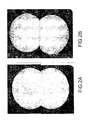
- the duration of the annealing depends on the volume of the sample to be annealed and the temperature chosen; in the case of a substrate of CdZnTe for example, brought to 1040 ° C, a duration of 5 minutes is sufficient to purge this substrate of the second phase that it contained, as shown by the Figures 2B and 3B .
- the estimated order of magnitude of these losses is, for example, for an initial sample of 5 grams, 1 gram of material Cd and Te lost for a few hundred micrograms of precipitates and inclusions.
- the tellurium precipitates are removed from a solid semiconductor material by the process according to the invention.
- the starting material is a CdTe solid developed at the maximum melting point.
- the monocrystalline substrate of dimensions 36 by 38 mm 2 and 750 ⁇ m thick is oriented along the axis [111]. Its surfaces are polished optical according to the usual procedure; they are then etched in a methanol solution containing 5% bromine just before the substrate is loaded into the suitable graphite crucible. The latter is then closed by a lid provided with a calibrated hole (diameter 2 mm). This semi-closed crucible is introduced into the annealing reactor, consisting of a quartz tube whose opening is closed by a sealed flange.
- thermocouple is positioned closest to the substrate in the graphite crucible.
- the quartz reactor is then evacuated and filled with argon at the pressure of 1 atmosphere.
- the reactor is, by subsequently, maintained under argon flotation at the rate of 100 cc / minute under the pressure of 1 atmosphere.
- the oven in which the quartz tube is installed is then heated and follows a thermal program imposed by the experimenter to reach the temperature of 1040 ° C, at a rate of 250 ° C / hour. It remains at this temperature for 5 minutes, before returning to room temperature at a rate of 40 ° C / hour.
- the epitaxial substrate is taken out of the crucible and is characterized by transmission IR microscopy, after a slight polishing made necessary following the evaporation undergone during the annealing phase.
- a field observed at a higher magnification shows precisely the shape, size and distribution of these black spots in the second phase.
- the Figure 2B shows the mapping of the same substrate after annealing according to the method of the invention, mapping carried out with a transmission infrared microscope. No black spots corresponding to a second phase are observed at room temperature. This is confirmed by the photograph taken at a higher magnification ( figure 3B ).
- the precipitates are removed from a ZnTe solid prepared in quartz tube sealed by the BRIDGMAN method as a telluric solvent and containing only telluride precipitates.
- a monocrystalline substrate of orientation [111] of dimensions 10 by 10 mm 2 and thickness 350 ⁇ m is treated in the same way as the previous CdTe; it is introduced into a graphite crucible similar to that used for the CdTe, which is positioned in the reactor flushed with argon flow with a flow rate of 100 cc / minute, under the pressure of 1 atmosphere.
- the annealing temperature can be chosen in the range of 449.5 ° C to 1240 ° C (maximum congruent evaporation temperature or temperature at which the congruent evaporation line intercepts the solidus ), according to the invention.
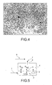
- the figure 4 shows a transmission image taken under an optical microscope (magnification 200) of a second phase free ZnTe wafer after annealing according to the method of the invention.
Landscapes
- Chemical & Material Sciences (AREA)
- Engineering & Computer Science (AREA)
- Crystallography & Structural Chemistry (AREA)
- Materials Engineering (AREA)
- Metallurgy (AREA)
- Organic Chemistry (AREA)
- Physics & Mathematics (AREA)
- Thermal Sciences (AREA)
- Inorganic Chemistry (AREA)
- Mechanical Engineering (AREA)
- Crystals, And After-Treatments Of Crystals (AREA)
- Semiconductor Lasers (AREA)
Claims (14)
- Verfahren zur Eliminierung der in einem festen II-VI-Halbleitermaterial enthaltenen Ausscheidungen durch Glühen, bei dem das feste Halbleitermaterial ein festes Halbleitermaterial mit kongruenter Sublimation ist, und bei dem man die folgenden sukzessiven Schritte durchführt:- man erhitzt das feste Halbleitermaterial unter Zirkulation von neutralem Gas bis auf eine Temperatur T, enthalten zwischen einer dem Eutektikum 11-VI-Verbindung/VI-Element entsprechenden ersten Temperatur T1 und einer der maximalen Temperatur kongruenter Sublimation entsprechenden zweiten Temperatur T2;- man hält das feste Material unter Zirkulation von neutralem Gas ausreichend lang auf dieser Temperatur T, um die Ausscheidungen zu eliminieren;- man kühlt das feste Material unter Zirkulation von neutralem Gas von der Temperatur T bis auf die Umgebungstemperatur mit einer solchen Geschwindigkeit ab, dass das feste Material im Laufe der Abkühlung genau seiner Linie der kongruenten Sublimation folgt;- man gewinnt das von Ausscheidungen befreite feste Halbleitermaterial.
- Verfahren nach Anspruch 1, bei dem die erste Temperatur T1 in dem Phasendiagramm des II-VI-Halbleitermaterials die dem Schnittpunkt der durch den maximalen Schmelzpunkt des Materials verlaufenden Vertikalen und der Soliduslinie entsprechende Temperatur ist.
- Verfahren nach einem der vorangehenden Ansprüche, bei dem die zweite Temperatur T2 in dem Phasendiagramm des II-VI-Halbleitermaterials die dem Schnittpunkt der Linie der kongruenten Sublimation und der Soliduslinie entsprechende Temperatur ist.
- Verfahren nach einem der vorangehenden Ansprüche, bei dem die Ausscheidungen Ausscheidungen des VI-Elements sind.
- Verfahren nach einem der vorangehenden Ansprüche, bei dem das II-VI-Halbleitermaterial ausgewählt wird unter CdTe, Cd1-xZnxTe, wo x von 0 bis 1 geht, und ZnTe.
- Verfahren nach Anspruch 5, bei dem das II-VI-Halbleitermaterial als Ausscheidungen nur Tellurausscheidungen enthält.
- Verfahren nach einem der vorangehenden Ansprüche, bei dem das Halbleitermaterial CdTe ist, die Ausscheidungen nur durch Tellur gebildet werden, die erste Temperatur T1 830°C und die zweite Temperatur T2 1 040°C beträgt.
- Verfahren nach einem der Ansprüche 1 bis 6, bei dem das Halbleitermaterial ZnTe ist, die Ausscheidungen nur durch Tellur gebildet werden, die erste Temperatur T1 820°C und die zweite Temperatur T2 1 240°C beträgt.
- Verfahren nach einem der vorangehenden Ansprüche, bei dem die Temperatur T während einer Dauer von 1 Minute bis 50 Stunden aufrechterhalten wird.
- Verfahren nach einem der vorangehenden Ansprüche, bei dem das Material ein einziges Substrat oder mehrere Substrate umfasst, wobei jedes dieser Substrate die Form eines Blocks oder Barrens aufweist.
- Verfahren nach einem der vorangehenden Ansprüche, bei dem das inerte Gas ausgewählt wird unter Argon und Helium.
- Verfahren nach einem der vorangehenden Ansprüche, bei dem das feste Halbleitermaterial ein durch ein BRIDGMAN-Verfahren am maximalen Schmelzpunkt oder aus VI-Element-Überschussschmelze hergestelltes Material ist.
- Verfahren nach einem der vorangehenden Ansprüche, bei dem das Material in einen wie eine KNUDSEN-Zelle konzipierten Tiegel gegeben wird.
- Verfahren nach einem der vorangehenden Ansprüche, bei dem das Verfahren in einem offenen Rohr, Reaktor realisiert wird.
Priority Applications (1)
| Application Number | Priority Date | Filing Date | Title |
|---|---|---|---|
| PL07115691T PL1897965T3 (pl) | 2006-09-07 | 2007-09-05 | Sposób eliminowania wydzieleń z materiału półprzewodnikowego II-VI za pomocą wygrzewania |
Applications Claiming Priority (1)
| Application Number | Priority Date | Filing Date | Title |
|---|---|---|---|
| FR0653612A FR2905706B1 (fr) | 2006-09-07 | 2006-09-07 | Procede d'elimination par recuit des precipites dans un materiau semi conducteur ii vi |
Publications (2)
| Publication Number | Publication Date |
|---|---|
| EP1897965A1 EP1897965A1 (de) | 2008-03-12 |
| EP1897965B1 true EP1897965B1 (de) | 2009-07-01 |
Family
ID=37671109
Family Applications (1)
| Application Number | Title | Priority Date | Filing Date |
|---|---|---|---|
| EP07115691A Active EP1897965B1 (de) | 2006-09-07 | 2007-09-05 | Verfahren zum Beseitigen von Ausscheidungen aus einem II-VI Halbleitermaterial durch Glühen. |
Country Status (8)
| Country | Link |
|---|---|
| US (1) | US8021482B2 (de) |
| EP (1) | EP1897965B1 (de) |
| JP (2) | JP6004601B2 (de) |
| AT (1) | ATE435312T1 (de) |
| DE (1) | DE602007001424D1 (de) |
| ES (1) | ES2329520T3 (de) |
| FR (1) | FR2905706B1 (de) |
| PL (1) | PL1897965T3 (de) |
Families Citing this family (7)
| Publication number | Priority date | Publication date | Assignee | Title |
|---|---|---|---|---|
| CN103114335B (zh) * | 2011-11-17 | 2016-04-27 | 通用电气公司 | 生产碲化镉或碲锌镉单晶体的方法 |
| EP2791054A4 (de) * | 2011-12-15 | 2016-03-09 | Midsummer Ab | Recycling von kupfer-indium-gallium-diselenid |
| JP6456782B2 (ja) * | 2015-06-23 | 2019-01-23 | Jx金属株式会社 | CdTe系化合物半導体単結晶及びその製造方法 |
| JP6448789B2 (ja) * | 2015-07-03 | 2019-01-09 | Jx金属株式会社 | CdTe系化合物単結晶及びその製造方法 |
| EP3923036A4 (de) | 2019-05-17 | 2022-11-02 | JX Nippon Mining & Metals Corporation | Halbleiterwafer, strahlungsdetektionselement, strahlungsdetektor und verfahren zur herstellung eines zusammengesetzten monokristallinen halbleitersubstrates |
| JP7250919B2 (ja) | 2019-05-17 | 2023-04-03 | Jx金属株式会社 | 半導体ウエハ、放射線検出素子、放射線検出器、及び化合物半導体単結晶基板の製造方法 |
| CN116040590A (zh) * | 2022-11-30 | 2023-05-02 | 宸亚(兰考县)科技有限公司 | 回收废碲化镉的工艺 |
Family Cites Families (25)
| Publication number | Priority date | Publication date | Assignee | Title |
|---|---|---|---|---|
| US3870473A (en) * | 1970-09-02 | 1975-03-11 | Hughes Aircraft Co | Tandem furnace crystal growing device |
| US4190486A (en) * | 1973-10-04 | 1980-02-26 | Hughes Aircraft Company | Method for obtaining optically clear, high resistivity II-VI, III-V, and IV-VI compounds by heat treatment |
| US4012242A (en) * | 1973-11-14 | 1977-03-15 | International Rectifier Corporation | Liquid epitaxy technique |
| JPS577171A (en) * | 1980-06-16 | 1982-01-14 | Junichi Nishizawa | Manufacture of znsepn junction |
| US4482423A (en) * | 1982-06-25 | 1984-11-13 | At&T Bell Laboratories | Protection of semiconductor substrates during epitaxial growth processes |
| US4481044A (en) * | 1982-11-29 | 1984-11-06 | Texas Instruments Incorporated | High-temperature Hg anneal for HgCdTe |
| JPS61106498A (ja) * | 1984-07-10 | 1986-05-24 | Yokogawa Hokushin Electric Corp | CdTeの結晶成長法 |
| JPS6287499A (ja) * | 1985-10-14 | 1987-04-21 | Nippon Mining Co Ltd | 単結晶CdTeの熱処理方法 |
| US4740386A (en) * | 1987-03-30 | 1988-04-26 | Rockwell International Corporation | Method for depositing a ternary compound having a compositional profile |
| EP0316161B1 (de) * | 1987-11-10 | 1994-01-19 | Kabushiki Kaisha Toshiba | Thermische Behandlung von einer II-VI-Halbleiterverbindung |
| JPH0259485A (ja) * | 1988-08-24 | 1990-02-28 | Matsushita Electric Ind Co Ltd | 結晶成長方法 |
| JPH0717477B2 (ja) * | 1989-03-15 | 1995-03-01 | シャープ株式会社 | 化合物半導体のエピタキシャル成長方法 |
| US5028296A (en) * | 1989-09-15 | 1991-07-02 | Texas Instruments Incorporated | Annealing method |
| JP2832241B2 (ja) * | 1989-10-09 | 1998-12-09 | 株式会社ジャパンエナジー | ▲ii▼―▲vi▼族化合物半導体結晶の製造方法 |
| US5041719A (en) * | 1990-06-01 | 1991-08-20 | General Electric Company | Two-zone electrical furnace for molecular beam epitaxial apparatus |
| US5201985A (en) * | 1991-03-07 | 1993-04-13 | Harald A.T.O. | Method and apparatus for the purification and control of the composition of non-stoichiometric and stoichiometric crystalline compounds |
| JP2746497B2 (ja) * | 1992-03-03 | 1998-05-06 | 三菱電機株式会社 | 半導体装置の製造方法 |
| US5599733A (en) * | 1993-10-15 | 1997-02-04 | Texas Instruments Incorporated | Method using cadmium-rich CdTe for lowering the metal vacancy concentrations of HgCdTe surfaces |
| DE69609568T2 (de) * | 1995-05-26 | 2001-02-01 | Sumitomo Electric Industries, Ltd. | Verfahren zur Herstellung von einem II-VI oder III-V Halbleitereinkristall |
| JP2839027B2 (ja) * | 1997-01-23 | 1998-12-16 | 住友電気工業株式会社 | Ii−vi族化合物半導体の熱処理方法 |
| JPH10212192A (ja) * | 1997-01-27 | 1998-08-11 | Japan Energy Corp | バルク結晶の成長方法 |
| JP3448688B2 (ja) * | 1998-05-11 | 2003-09-22 | 株式会社ジャパンエナジー | CdTe結晶またはCdZnTe結晶およびその製造方法 |
| US6613162B1 (en) * | 1999-10-25 | 2003-09-02 | Rensselaer Polytechnic Institute | Multicomponent homogeneous alloys and method for making same |
| JP2001332506A (ja) * | 2000-05-19 | 2001-11-30 | Sumitomo Electric Ind Ltd | ZnSe結晶基板の熱処理方法、熱処理基板及び発光素子 |
| JP2003124235A (ja) * | 2001-10-17 | 2003-04-25 | Sumitomo Electric Ind Ltd | Ii−vi族化合物半導体、その熱処理方法およびその熱処理装置 |
-
2006
- 2006-09-07 FR FR0653612A patent/FR2905706B1/fr not_active Expired - Fee Related
-
2007
- 2007-09-05 ES ES07115691T patent/ES2329520T3/es active Active
- 2007-09-05 AT AT07115691T patent/ATE435312T1/de not_active IP Right Cessation
- 2007-09-05 PL PL07115691T patent/PL1897965T3/pl unknown
- 2007-09-05 EP EP07115691A patent/EP1897965B1/de active Active
- 2007-09-05 DE DE602007001424T patent/DE602007001424D1/de active Active
- 2007-09-06 US US11/851,051 patent/US8021482B2/en active Active
- 2007-09-06 JP JP2007231529A patent/JP6004601B2/ja active Active
-
2014
- 2014-10-23 JP JP2014216109A patent/JP2015038035A/ja active Pending
Also Published As
| Publication number | Publication date |
|---|---|
| JP2015038035A (ja) | 2015-02-26 |
| PL1897965T3 (pl) | 2009-12-31 |
| EP1897965A1 (de) | 2008-03-12 |
| US20080060729A1 (en) | 2008-03-13 |
| FR2905706B1 (fr) | 2009-04-17 |
| DE602007001424D1 (de) | 2009-08-13 |
| FR2905706A1 (fr) | 2008-03-14 |
| ATE435312T1 (de) | 2009-07-15 |
| JP6004601B2 (ja) | 2016-10-12 |
| JP2008100900A (ja) | 2008-05-01 |
| ES2329520T3 (es) | 2009-11-26 |
| US8021482B2 (en) | 2011-09-20 |
Similar Documents
| Publication | Publication Date | Title |
|---|---|---|
| EP1897965B1 (de) | Verfahren zum Beseitigen von Ausscheidungen aus einem II-VI Halbleitermaterial durch Glühen. | |
| EP0801155B1 (de) | Verfahren und Vorrichtung zur Herstellung einkristallines Siliziumkarbids (SiC) auf einem Keimkristall | |
| FR2543981A1 (fr) | Procede de fabrication de materiaux semi-conducteurs et four de traitement pour la mise en oeuvre de ce procede | |
| EP0034982B1 (de) | Verfahren zur Herstellung homogener Schichten aus Hg1-xCdxTe | |
| FR2589489A1 (fr) | Substrat de silicium monocristallin et ses procedes et appareil de fabrication | |
| EP3184673B1 (de) | Verfahren zum einstellen eines brennofens, der für das formen von wärmespendern verwendet wird | |
| EP1415023B1 (de) | Verfahren zur herstellung eines einkristalles aus cdte oder cdznte | |
| FR3083917A1 (fr) | Procede de production d’une tranche collee de silicium et tranche collee de silicium | |
| US6143630A (en) | Method of impurity gettering | |
| EP2581475A1 (de) | Verfahren zur Herstellung von p-dotiertem Zinkoxyd ZnO oder von p-dotiertem ZnMgO | |
| Kalisher et al. | Hg-rich liquid-phase epitaxy of Hg1− xCdxTe | |
| EP2154712A1 (de) | Vorbereitungsverfahren eines ZnO-Substrats, das ganz oder teilweise quasi-isolierend oder mit Typ P dotiert ist, so erhaltene Substrate und elektronische, elektrooptische oder optoelektronische Vorrichtungen, die sie enthalten | |
| EP0234984B1 (de) | Verfahren zum Herstellen eines kristallinen Hg1-xo Cdxo Te-Stab | |
| EP2319072A1 (de) | Verfahren zur herstellung eines selbstunterstützenden kristallisierten siliziumdünnfilms | |
| FR3060843B1 (fr) | Methode de fabrication d'une tranche de silicium a jonction p-n et tranche de silicium a jonction p-n | |
| EP2363515A1 (de) | Herstellungsverfahren eines kristallisierten Halbleitermaterials | |
| EP0209629B1 (de) | Verfahren zur Herstellung einer Lösungszone zum Züchten von Halbleiterverbindungen | |
| WO2013050927A1 (fr) | Procede de formation d'une couche de silicium cristallisee en surface de plusieurs substrats | |
| WO2012073205A1 (fr) | Procede de preparation d'une couche de silicium cristallise a gros grains | |
| FR2985722A1 (fr) | Procede de purification du silicium. | |
| FR3091008A1 (fr) | Substrat semi-conducteur avec couche intermédiaire dopée n | |
| FR2661195A1 (fr) | Procede et appareil de croissance hetero-epitaxiale en phase liquide. | |
| EP1713958B1 (de) | Verfahren und vorrichtung zur herstellung von einkristallen | |
| Sreedhar | Liquid phase epitaxial growth from Te-rich solutions and junction formation in | |
| FR2763608A1 (fr) | Nacelle d'epitaxie pour depot d'une couche de cdhgte par epitaxie en phase liquide sur un heterosubstrat et procede de depot de cdhgte sur un heterosubstrat utilisant cette nacelle |
Legal Events
| Date | Code | Title | Description |
|---|---|---|---|
| PUAI | Public reference made under article 153(3) epc to a published international application that has entered the european phase |
Free format text: ORIGINAL CODE: 0009012 |
|
| AK | Designated contracting states |
Kind code of ref document: A1 Designated state(s): AT BE BG CH CY CZ DE DK EE ES FI FR GB GR HU IE IS IT LI LT LU LV MC MT NL PL PT RO SE SI SK TR |
|
| AX | Request for extension of the european patent |
Extension state: AL BA HR MK YU |
|
| 17P | Request for examination filed |
Effective date: 20080729 |
|
| AKX | Designation fees paid |
Designated state(s): AT BE BG CH CY CZ DE DK EE ES FI FR GB GR HU IE IS IT LI LT LU LV MC MT NL PL PT RO SE SI SK TR |
|
| GRAP | Despatch of communication of intention to grant a patent |
Free format text: ORIGINAL CODE: EPIDOSNIGR1 |
|
| GRAS | Grant fee paid |
Free format text: ORIGINAL CODE: EPIDOSNIGR3 |
|
| GRAA | (expected) grant |
Free format text: ORIGINAL CODE: 0009210 |
|
| AK | Designated contracting states |
Kind code of ref document: B1 Designated state(s): AT BE BG CH CY CZ DE DK EE ES FI FR GB GR HU IE IS IT LI LT LU LV MC MT NL PL PT RO SE SI SK TR |
|
| REG | Reference to a national code |
Ref country code: GB Ref legal event code: FG4D Free format text: NOT ENGLISH |
|
| REG | Reference to a national code |
Ref country code: CH Ref legal event code: EP |
|
| REG | Reference to a national code |
Ref country code: IE Ref legal event code: FG4D |
|
| REF | Corresponds to: |
Ref document number: 602007001424 Country of ref document: DE Date of ref document: 20090813 Kind code of ref document: P |
|
| REG | Reference to a national code |
Ref country code: ES Ref legal event code: FG2A Ref document number: 2329520 Country of ref document: ES Kind code of ref document: T3 |
|
| PG25 | Lapsed in a contracting state [announced via postgrant information from national office to epo] |
Ref country code: SI Free format text: LAPSE BECAUSE OF FAILURE TO SUBMIT A TRANSLATION OF THE DESCRIPTION OR TO PAY THE FEE WITHIN THE PRESCRIBED TIME-LIMIT Effective date: 20090701 |
|
| NLV1 | Nl: lapsed or annulled due to failure to fulfill the requirements of art. 29p and 29m of the patents act | ||
| REG | Reference to a national code |
Ref country code: PL Ref legal event code: T3 |
|
| PG25 | Lapsed in a contracting state [announced via postgrant information from national office to epo] |
Ref country code: FI Free format text: LAPSE BECAUSE OF FAILURE TO SUBMIT A TRANSLATION OF THE DESCRIPTION OR TO PAY THE FEE WITHIN THE PRESCRIBED TIME-LIMIT Effective date: 20090701 Ref country code: EE Free format text: LAPSE BECAUSE OF FAILURE TO SUBMIT A TRANSLATION OF THE DESCRIPTION OR TO PAY THE FEE WITHIN THE PRESCRIBED TIME-LIMIT Effective date: 20090701 Ref country code: IS Free format text: LAPSE BECAUSE OF FAILURE TO SUBMIT A TRANSLATION OF THE DESCRIPTION OR TO PAY THE FEE WITHIN THE PRESCRIBED TIME-LIMIT Effective date: 20091101 Ref country code: LT Free format text: LAPSE BECAUSE OF FAILURE TO SUBMIT A TRANSLATION OF THE DESCRIPTION OR TO PAY THE FEE WITHIN THE PRESCRIBED TIME-LIMIT Effective date: 20090701 Ref country code: AT Free format text: LAPSE BECAUSE OF FAILURE TO SUBMIT A TRANSLATION OF THE DESCRIPTION OR TO PAY THE FEE WITHIN THE PRESCRIBED TIME-LIMIT Effective date: 20090701 Ref country code: SE Free format text: LAPSE BECAUSE OF FAILURE TO SUBMIT A TRANSLATION OF THE DESCRIPTION OR TO PAY THE FEE WITHIN THE PRESCRIBED TIME-LIMIT Effective date: 20090701 |
|
| REG | Reference to a national code |
Ref country code: IE Ref legal event code: FD4D |
|
| PG25 | Lapsed in a contracting state [announced via postgrant information from national office to epo] |
Ref country code: LV Free format text: LAPSE BECAUSE OF FAILURE TO SUBMIT A TRANSLATION OF THE DESCRIPTION OR TO PAY THE FEE WITHIN THE PRESCRIBED TIME-LIMIT Effective date: 20090701 Ref country code: NL Free format text: LAPSE BECAUSE OF FAILURE TO SUBMIT A TRANSLATION OF THE DESCRIPTION OR TO PAY THE FEE WITHIN THE PRESCRIBED TIME-LIMIT Effective date: 20090701 |
|
| BERE | Be: lapsed |
Owner name: COMMISSARIAT A L'ENERGIE ATOMIQUE Effective date: 20090930 |
|
| PG25 | Lapsed in a contracting state [announced via postgrant information from national office to epo] |
Ref country code: PT Free format text: LAPSE BECAUSE OF FAILURE TO SUBMIT A TRANSLATION OF THE DESCRIPTION OR TO PAY THE FEE WITHIN THE PRESCRIBED TIME-LIMIT Effective date: 20091102 Ref country code: BG Free format text: LAPSE BECAUSE OF FAILURE TO SUBMIT A TRANSLATION OF THE DESCRIPTION OR TO PAY THE FEE WITHIN THE PRESCRIBED TIME-LIMIT Effective date: 20091001 |
|
| PG25 | Lapsed in a contracting state [announced via postgrant information from national office to epo] |
Ref country code: RO Free format text: LAPSE BECAUSE OF FAILURE TO SUBMIT A TRANSLATION OF THE DESCRIPTION OR TO PAY THE FEE WITHIN THE PRESCRIBED TIME-LIMIT Effective date: 20090701 Ref country code: DK Free format text: LAPSE BECAUSE OF FAILURE TO SUBMIT A TRANSLATION OF THE DESCRIPTION OR TO PAY THE FEE WITHIN THE PRESCRIBED TIME-LIMIT Effective date: 20090701 Ref country code: IE Free format text: LAPSE BECAUSE OF FAILURE TO SUBMIT A TRANSLATION OF THE DESCRIPTION OR TO PAY THE FEE WITHIN THE PRESCRIBED TIME-LIMIT Effective date: 20090701 Ref country code: MC Free format text: LAPSE BECAUSE OF NON-PAYMENT OF DUE FEES Effective date: 20090930 |
|
| PLBE | No opposition filed within time limit |
Free format text: ORIGINAL CODE: 0009261 |
|
| STAA | Information on the status of an ep patent application or granted ep patent |
Free format text: STATUS: NO OPPOSITION FILED WITHIN TIME LIMIT |
|
| PG25 | Lapsed in a contracting state [announced via postgrant information from national office to epo] |
Ref country code: SK Free format text: LAPSE BECAUSE OF FAILURE TO SUBMIT A TRANSLATION OF THE DESCRIPTION OR TO PAY THE FEE WITHIN THE PRESCRIBED TIME-LIMIT Effective date: 20090701 |
|
| 26N | No opposition filed |
Effective date: 20100406 |
|
| PG25 | Lapsed in a contracting state [announced via postgrant information from national office to epo] |
Ref country code: BE Free format text: LAPSE BECAUSE OF NON-PAYMENT OF DUE FEES Effective date: 20090930 |
|
| PG25 | Lapsed in a contracting state [announced via postgrant information from national office to epo] |
Ref country code: GR Free format text: LAPSE BECAUSE OF FAILURE TO SUBMIT A TRANSLATION OF THE DESCRIPTION OR TO PAY THE FEE WITHIN THE PRESCRIBED TIME-LIMIT Effective date: 20091002 |
|
| PG25 | Lapsed in a contracting state [announced via postgrant information from national office to epo] |
Ref country code: LU Free format text: LAPSE BECAUSE OF NON-PAYMENT OF DUE FEES Effective date: 20090905 Ref country code: MT Free format text: LAPSE BECAUSE OF FAILURE TO SUBMIT A TRANSLATION OF THE DESCRIPTION OR TO PAY THE FEE WITHIN THE PRESCRIBED TIME-LIMIT Effective date: 20090701 |
|
| PG25 | Lapsed in a contracting state [announced via postgrant information from national office to epo] |
Ref country code: HU Free format text: LAPSE BECAUSE OF FAILURE TO SUBMIT A TRANSLATION OF THE DESCRIPTION OR TO PAY THE FEE WITHIN THE PRESCRIBED TIME-LIMIT Effective date: 20100102 |
|
| PG25 | Lapsed in a contracting state [announced via postgrant information from national office to epo] |
Ref country code: TR Free format text: LAPSE BECAUSE OF FAILURE TO SUBMIT A TRANSLATION OF THE DESCRIPTION OR TO PAY THE FEE WITHIN THE PRESCRIBED TIME-LIMIT Effective date: 20090701 |
|
| PG25 | Lapsed in a contracting state [announced via postgrant information from national office to epo] |
Ref country code: CY Free format text: LAPSE BECAUSE OF FAILURE TO SUBMIT A TRANSLATION OF THE DESCRIPTION OR TO PAY THE FEE WITHIN THE PRESCRIBED TIME-LIMIT Effective date: 20090701 |
|
| REG | Reference to a national code |
Ref country code: CH Ref legal event code: PL |
|
| PG25 | Lapsed in a contracting state [announced via postgrant information from national office to epo] |
Ref country code: CH Free format text: LAPSE BECAUSE OF NON-PAYMENT OF DUE FEES Effective date: 20110930 Ref country code: LI Free format text: LAPSE BECAUSE OF NON-PAYMENT OF DUE FEES Effective date: 20110930 |
|
| REG | Reference to a national code |
Ref country code: FR Ref legal event code: PLFP Year of fee payment: 10 |
|
| REG | Reference to a national code |
Ref country code: FR Ref legal event code: PLFP Year of fee payment: 11 |
|
| REG | Reference to a national code |
Ref country code: FR Ref legal event code: PLFP Year of fee payment: 12 |
|
| PGFP | Annual fee paid to national office [announced via postgrant information from national office to epo] |
Ref country code: DE Payment date: 20250919 Year of fee payment: 19 |
|
| PGFP | Annual fee paid to national office [announced via postgrant information from national office to epo] |
Ref country code: PL Payment date: 20250825 Year of fee payment: 19 |
|
| PGFP | Annual fee paid to national office [announced via postgrant information from national office to epo] |
Ref country code: GB Payment date: 20250923 Year of fee payment: 19 |
|
| PGFP | Annual fee paid to national office [announced via postgrant information from national office to epo] |
Ref country code: FR Payment date: 20250924 Year of fee payment: 19 |
|
| PGFP | Annual fee paid to national office [announced via postgrant information from national office to epo] |
Ref country code: CZ Payment date: 20250827 Year of fee payment: 19 |
|
| PGFP | Annual fee paid to national office [announced via postgrant information from national office to epo] |
Ref country code: IT Payment date: 20250930 Year of fee payment: 19 |
|
| PGFP | Annual fee paid to national office [announced via postgrant information from national office to epo] |
Ref country code: ES Payment date: 20251020 Year of fee payment: 19 |