EP1898667A2 - Mikrophonbaugruppe - Google Patents
Mikrophonbaugruppe Download PDFInfo
- Publication number
- EP1898667A2 EP1898667A2 EP07017238A EP07017238A EP1898667A2 EP 1898667 A2 EP1898667 A2 EP 1898667A2 EP 07017238 A EP07017238 A EP 07017238A EP 07017238 A EP07017238 A EP 07017238A EP 1898667 A2 EP1898667 A2 EP 1898667A2
- Authority
- EP
- European Patent Office
- Prior art keywords
- microphone
- chip
- sound hole
- lsi chip
- substrate
- Prior art date
- Legal status (The legal status is an assumption and is not a legal conclusion. Google has not performed a legal analysis and makes no representation as to the accuracy of the status listed.)
- Withdrawn
Links
Images



Classifications
-
- H—ELECTRICITY
- H04—ELECTRIC COMMUNICATION TECHNIQUE
- H04R—LOUDSPEAKERS, MICROPHONES, GRAMOPHONE PICK-UPS OR LIKE ACOUSTIC ELECTROMECHANICAL TRANSDUCERS; ELECTRIC HEARING AIDS; PUBLIC ADDRESS SYSTEMS
- H04R19/00—Electrostatic transducers
- H04R19/01—Electrostatic transducers characterised by the use of electrets
- H04R19/016—Electrostatic transducers characterised by the use of electrets for microphones
-
- H—ELECTRICITY
- H04—ELECTRIC COMMUNICATION TECHNIQUE
- H04R—LOUDSPEAKERS, MICROPHONES, GRAMOPHONE PICK-UPS OR LIKE ACOUSTIC ELECTROMECHANICAL TRANSDUCERS; ELECTRIC HEARING AIDS; PUBLIC ADDRESS SYSTEMS
- H04R19/00—Electrostatic transducers
- H04R19/04—Microphones
-
- H—ELECTRICITY
- H04—ELECTRIC COMMUNICATION TECHNIQUE
- H04R—LOUDSPEAKERS, MICROPHONES, GRAMOPHONE PICK-UPS OR LIKE ACOUSTIC ELECTROMECHANICAL TRANSDUCERS; ELECTRIC HEARING AIDS; PUBLIC ADDRESS SYSTEMS
- H04R1/00—Details of transducers, loudspeakers or microphones
- H04R1/02—Casings; Cabinets ; Supports therefor; Mountings therein
- H04R1/04—Structural association of microphone with electric circuitry therefor
-
- H—ELECTRICITY
- H04—ELECTRIC COMMUNICATION TECHNIQUE
- H04R—LOUDSPEAKERS, MICROPHONES, GRAMOPHONE PICK-UPS OR LIKE ACOUSTIC ELECTROMECHANICAL TRANSDUCERS; ELECTRIC HEARING AIDS; PUBLIC ADDRESS SYSTEMS
- H04R31/00—Apparatus or processes specially adapted for the manufacture of transducers or diaphragms therefor
- H04R31/006—Interconnection of transducer parts
Definitions
- the present invention relates to microphone packages encapsulating microphones such as silicon condenser microphones.
- Japanese Patent Application Publication No. 2004-537182 teaches an example of a microphone package, in which a miniature silicon condenser microphone is encapsulated in a housing having a cavity and a sound hole communicating with the exterior, wherein a microphone chip (for detecting sound) and an LSI chip (for controlling the microphone chip) are mounted on the mounting surface of the housing by use of a die-bonding material.
- This type of microphone package can be redesigned such that the LSI chip is sealed with a resin (or a potting material), by which the LSI chip is protected
- it can be redesigned such that the sound hole is opened on the mounting surface of the housing for mounting the microphone chip and LSI chip.
- the sound hole opened on the mounting surface of the housing for mounting the microphone chip may likely allow the "liquid” die-bonding material and the "liquid” potting material to flow into the inside during the manufacturing.
- a microphone package includes a housing having a cavity and a sound hole allowing the cavity to communicate with the exterior, and a microphone chip mounted on the mounting surface so as to detect sound within the cavity; and a projection wall that projects upwardly from the mounting surface at the prescribed position between the sound hole and the microphone chip.
- a liquid die-bonding material is applied to the prescribed position for mounting the microphone chip on the mounting surface, wherein it is possible to prevent the liquid die-bonding material from flowing over the mounting surface by means of the projection wall. Therefore, even when the distance between the microphone chip and the sound hole is reduced, it is possible to prevent the liquid die-bonding material from flowing into the sound hole.
- the projection wall blocks the light incident into the sound hole; hence, it is possible to easily prevent the incident light from reaching the microphone chip composed of silicon.
- the sound hole is surrounded by the projection wall, by which it is possible to reliably prevent the liquid die-bonding material from unexpectedly flowing into the sound hole.
- the prescribed portion of an external connection wire is electrically connected to the microphone chip and is exposed on the upper surface of the projection wall. This makes it possible to prevent the liquid die-bonding material from covering the prescribed portion of the external connection wire when the microphone chip is fixed onto the mounting surface; thereafter, it is possible to easily establish an electrical connection between the microphone chip and the prescribed portion of the external connection wire. Furthermore, when an LSI chip for driving the controlling of the microphone chip is fixed onto the mounting surface, it is possible to reduce the difference between the height of an electrode pad formed on the upper surface of the microphone chip or the upper surface of the LSI chip and the height of the prescribed portion of the external connection wire. This makes it possible to easily perform wire bonding using a capillary between the electrode pad and the prescribed portion of the external connection wire.
- the projection wall is further increased in height between the sound hole and the prescribed portion of the external connection wire. That is, when both of the LSI chip mounted on the mounting surface and the prescribed portion of the external connection wire electrically connected to the electrode pad are sealed with a resin (or a potting material), it is possible to prevent the potting material from flowing over the mounting surface by means of the projection wall; hence, it is possible to reliably prevent the potting material from flowing into the sound hole.
- the sound hole is surrounded by the projection wall further increased in height. This makes it possible to reliably prevent the potting material from flowing into the sound hole.
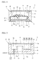
- a microphone package 1 according to a preferred embodiment of the present invention will be described with reference to FIGS. 1 to 5.
- the microphone package 1 is constituted of a substrate 3, a microphone chip 5 arranged in connection with a surface 3a of the substrate 3, an LSI chip 7, and a cover board 9.
- the substrate 3 is shaped like a plate having a rectangular shape in plan view, in which a plurality of recesses 11 are formed on a side wall 3b and are each opened in both of the surface 3a and a backside 3c.
- the microphone chip 5 and the LSI chip 7 are arranged on a bottom 13a (i.e., a mounting surface) of the hollow portion 13.
- a step portion 15 (or a wall) is formed and elongated along one side of the alignment of the microphone chip 5 and the LSI chip 7, wherein the step portion 15 projects upwardly from the bottom 13a of the hollow portion 13.
- the step portion 15 forms a step-like height difference between the bottom 13a of the hollow portion 13 and the surface 3a of the substrate 3.
- the substrate 3 is a multilayered wiring substrate composed of ceramics. As shown in FIGS. 2, 4 and 5, a plurality of external connection wires 17 are formed so as to electrically connect the microphone chip 5 and the LSI chip 7 to a circuit board (not shown) for mounting the microphone package 1.
- each of the external connection wires 17 includes a first portion that is exposed on an upper surface 15a of the step portion 15 so as to form an internal terminal 19, which is electrically connected to the LSI chip 7, a second portion that is exposed on the backside 3c of the substrate 3 so as to form an external terminal 21, which is electrically connected to the circuit board, and a third portion that is elongated inside of the substrate 3 so as to form a conductive portion 23 for electrically connecting the internal terminal 19 and the external terminal 21.
- the internal terminal 19A serves as a power terminal
- the internal terminal 19B serves as an output signal terminal
- the internal terminal 19C serves as a gain control terminal
- the internal terminal 19D serves as a ground terminal.
- the ground terminal 19D is electrically connected to a ground conduction portion 23D, which is formed on the upper surface 15a of the step portion 15 in proximity to the microphone chip 5.
- the ground conduction portion 23D runs through the step portion 15 from the upper surface 15a to the backside 3a of the substrate 3 and is electrically connected to a ground external terminal 21 D.
- a ring-shaped connection pad 25 is formed on the surface 3a of the substrate 3. As shown in FIG. 2, a prescribed part of the ring-shaped connection pad 25 is horizontally elongated to reach a single recess 11 A within the recesses 11 formed on the side walls 3b of the side wall 3b of the substrate 3. A conduction portion (not shown) is formed on the interior wall of the recess 11A. Thus, the ring-shaped connection pad 25 is electrically connected to the ground external terminal 21 D, which is formed on the backside 3c of the substrate 3, via the conduction portion.
- the external connection wires 17, the connection pad 25, and the conduction portion formed inside of the recess 11A are each formed by way of screen printing using a paste that is mainly composed of silver powder, copper powder, or tungsten powder, or using a paste in which binders (or acrylic resins) are mixed with the silver powder, copper powder, or tungsten powder.
- the internal terminals 19 exposed on the upper surface 15a of the step portion 15 are each formed by way of nickel and gold plating on the aforementioned materials.
- the external terminals 21 exposed on the backside 3c of the substrate 3 are each formed by way of nickel and gold plating on the aforementioned materials.
- a sound hole 27 runs through the substrate 3 from the backside 3c to the inside of the hollow portion 13.
- the sound hole 27 is opened on the upper surface 15a of the step portion 15 at a prescribed position between the internal terminals 19 and the ground conduction portion 23D. That is, the sound hole 27 is surrounded and defined by the step portion 15 that projects upwardly from the bottom 13a of the hollow portion 13.
- a rectangular-shaped projection wall 29 projects upwardly from the upper surface 15a of the step portion 15 so as to vertically elongate and surround the sound hole 27.
- the distal end of the projection wall 29 is positioned at a height lower than the surface 3a of the substrate 3.
- the cover board 9 is formed by performing nickel plating on a board composed of a conductive material such as copper. As shown FIGS. 3 to 5, the cover board 9 is fixed onto the surface 3a of the substrate 3 so as to cover the opening of the hollow portion 13, thus forming a cavity S 1 embracing the microphone chip 5 and the LSI chip 7 together with the substrate 3.
- the cavity S1 communicates with the exterior via the sound hole 27 formed in the substrate 3.
- the cover board 9 comes in contact with the connection pad 25 having conductivity and is thus electrically connected to the connection pad 25. That is, the cover board 9 is electrically connected to the ground external terminal 21D via the connection pad 25 and the conduction portion of the recess 11 A.
- the substrate 3 and the cover board 9 are combined together so as to form a housing 31 having the cavity S1 and the sound hole 27.
- the microphone chip 5 includes a diaphragm 35 (composed of silicon), which covers an inner hole 33a of a ring-shaped support 33.
- the diaphragm 35 detects sound by way of vibration thereof; hence, the microphone chip 5 forms a sound pressure sensor chip for converting the vibration of the diaphragm 35 into electric signals.
- the microphone chip 5 is fixed onto the bottom 13a of the hollow portion 13 of the substrate 3 via a die-bonding material (not shown) in such a way that the diaphragm 35 is positioned opposite to the bottom 13a via the inner hole 33a.
- An upper surface 5a of the microphone chip 5, which is fixed to the bottom 13a, is set to a prescribed height such that it is higher than the upper surface 15a of the step portion 15 but is lower than the distal end of the projection wall 29.
- the LSI chip 7 drives and controls the microphone chip 5.
- the LSI chip 7 includes an amplification circuit for amplifying electric signals output from the microphone chip 5. Similar to the microphone chip 5, the LSI chip 7 is fixed onto the bottom 13a of the hollow portion 13 of the substrate 3 via a die-bonding material (not shown). As shown in FIGS. 3 and 4, an upper surface 7a of the LSI chip 7, which is fixed to the bottom 13a, is set to a prescribed height substantially identical to the height of the upper surface 15a of the step portion 15.
- a single electrode pad 7b formed on the upper surface 7a of the LSI chip 7 is electrically connected to an electrode pad 5b formed on the upper surface 5a of the microphone chip 5 via a first wire 37.
- Other electrode pads 7c of the LSI chip 7 are each electrically connected to the internal terminals 19 via second wires 39.
- the microphone chip 5 is electrically connected to the external connection wires 17 via the LSI chip 7.
- the LSI chip 7, the internal terminal 19, a part of the first wire 37, and the second wires 39 are sealed with a resin sealing portion 41 formed above the bottom 13a of the hollow portion 13 of the substrate 3.
- the resin material (or potting material) forming the resin sealing portion 41 it is possible to use a silicon resin or an epoxy resin.
- the height of the resin sealing portion 41 is set such that the top portion thereof is lower than the upper surface 5a of the microphone chip 5 and the distal end of the projection wall 29.
- the substrate 3 is produced in advance.
- Each substrate 3, can be individually produced in advance. Instead, a plurality of substrates 3 are combined and collectively produced in advance, and then they are each divided into individual pieces, for example.
- a plurality of through-holes running through the thickness direction are formed between adjacently arranged substrates 3, and then the substrates 3 are each divided into individual pieces by way of breakage along the through-holes.
- the liquid die-bonding material is applied to prescribed positions for mounting the microphone chip 5 and the LSI chip 7 on the bottom 13a of the hollow portion 13 of the substrate 3; then, it is hardened while the microphone chip 5 and the LSI chip 7 are arranged at the prescribed positions respectively; thus, the microphone chip 5 and the LSI chip 7 are firmly fixed onto the bottom 13a. In this process, even when the liquid die-bonding material flows over the bottom 13a, it is stopped at the step portion 15.
- wire bonding is performed using a capillary (not shown), so that the first wire 37 is formed between the electrode pad 5b of the microphone chip 5 and the electrode pad 7b of the LSI chip 7, and the second wires 39 are formed between the other electrode pads 7c of the LSI chip 7 and the internal terminals 19.
- the wire bonding can be easily performed because both of the upper surface 7a of the LSI chip 7 and the upper surface 15a of the step portion 15 are substantially set to the same height.
- the liquid potting material is introduced into the hollow portion 13 of the substrate 3 from the upper side of the LSI chip 7; then, the liquid potting material is hardened so as to form the resin sealing portion 41 for sealing the LSI chip 7, the internal terminals 19, a part of the first wire 37, and the second wires 39. In this process, even when the liquid potting material flows over the bottom 13a and the upper surface 15a of the step portion 15, it is stopped at the projection wall 29.
- both of the upper surface 5a of the microphone chip 5 and the distal end of the projection wall 29 are higher than the upper surface 7a of the LSI chip 7 and the upper surface 15a of the step portion 15. Therefore, by adjusting the amount of the potting material to be introduced into the hollow portion 13 of the substrate 3, it is possible to easily prevent the potting material from unexpectedly covering the upper surface 5a of the microphone chip 5 and to easily prevent the potting material from unexpectedly flowing into the sound hole 27.
- the cover board 9 is fixed onto the surface 3a of the substrate 3 by use of the conductive adhesive, thus completing the manufacturing of the microphone package 1.
- both of the upper surface 15a of the step portion 15 and the upper surface 7a of the LSI chip 7 are set to substantially the same height.
- the cover board 9 is electrically connected to the ground external terminal 21D, which is then connected to a ground pattern of a circuit board (not shown). This makes it possible for the cover board 9 to block electromagnetic noise occurring outside of the microphone package 1. That is, it is possible to reliably prevent electromagnetic noise from unexpectedly reaching the microphone chip 5; hence, it is possible to avoid the erroneous operation of the microphone chip 5 due to electromagnetic noise.
- the present embodiment is designed such that the upper surface 15a of the step portion 15, which projects upwardly from the bottom 13a, is set to substantially the same height as the upper surface 7a of the LSI chip 7; but this is not a restriction. That is, it is simply required to reduce the difference between the height of the upper surface 15a of the step portion 15 and the height of the upper surface 7a of the LSI chip 7. Due to the reduced difference between their heights, it is possible to easily perform wire bonding between the LSI chip 7 and the internal terminals 19.
- the present embodiment is designed such that the ring-shaped projection wall 29 surrounding the sound hole 27 further projects upwardly from the upper surface 15a of the step portion 15; but this is not a restriction. It is simply required that the projection wall 29 be formed between the ground conduction portion 23D and the internal terminals 19, both of which are formed by means of the external connection wires 17. This constitution can reliably stop the flow of the liquid potting material by means of the projection wall 29; hence, it is possible to reliably prevent the liquid potting material from flowing into the sound hold 27.
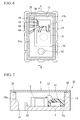
- the present embodiment can be modified such that, without forming the projection wall 29 projecting upwardly from the step portion 15, the sound hole 27 is directly opened on the upper surface 15a of the step portion 15. That is, it is preferable that, in a microphone package 51 shown in FIGS. 6 and 7, a sound hole 53 be formed between the LSI chip 7 and the microphone chip 5.
- This constitution increases the region for forming the microphone chip 5 because the microphone chip 5 is sandwiched between the LSI chip 7 and a step portion (or a projection wall) 55 projecting upwardly from the bottom 13a of the hollow portion 13 of the substrate 3.
- the sound hole 53 is formed along the alignment of the microphone chip 5 and the LSI chip 7, it is possible to increase the overall size of the microphone package 51 in the modification shown in FIGS. 6 and 7 compared with the present embodiment.
- the sound hole 53 is distanced from the LSI chip 7; hence, it is possible to adequately prevent the liquid potting material from unexpectedly flowing into the sound hole 53 without forming a projection wall projecting upwardly from an upper surface 55a of the step portion 55.
- the microphone package 51 in which the step portion 55 is enlarged to sandwich the microphone chip 5 with the LSI chip 7, can be further modified as a microphone package 61 as shown in FIGS. 8 and 9, in which a bottomed recess 63, which is recessed from the upper surface 55a of the step portion 55, is formed in the periphery of the sound hole 53.
- the microphone package 61 has a substrate 65, which is designed such that the thickness at a first end 65d forming the step portion 55 is larger than the thickness at a second end 65e arranging the LSI chip 7, wherein due to the formation of the bottomed recess 63, it is possible to realize substantially the same rigidity at both of the first end 65d and the second end 65e. For this reason, when a plurality of substrates 65 are combined and collectively produced and are then subjected to bending along scribing regions, it is possible to easily divide the individual substrates 65 by concentrating stress at the scribing regions.
- the aforementioned microphone packages 1,51, and 61 are designed such that the sound holes 27 and 53 are opened on the upper surfaces 15a and 55a of the step portions 15 and 55; but this is not a restriction. That is, the sound holes 27 and 53 can be directly opened on the bottoms 13a of the substrates 3 and 65, wherein ring-shaped walls, which are formed independently of the step portions 15 and 55, are formed to project upwardly from the bottoms 13a of the substrates 3 and 65 in the peripheries of the sound holes 27 and 53.
- the aforementioned walls are not necessarily formed in ring shapes, and it is simply required that they are each formed between the microphone chip 5, the LSI chip 7, and the sound holes 27 and 53.
- the height of the wall formed between the LSI chip 7 and each of the sound holes 27 and 53 be higher than the height of the LSI chip 7 so as to secure the formation of the resin sealing portion 41.
- All the microphone packages 1,51, and 61 are each equipped with the LSI chip 7; but this is not a restriction. That is, it is simply required that each microphone package be equipped with the microphone chip 5, and that the electrode pads 5b of the microphone chip 5 be directly electrically connected to the internal terminals 19 via wires. In this constitution, the internal terminals 19 are still formed on the upper surfaces 15a and 55a of the step portion 15 and 55; this makes it possible to reduce the height differences between the internal terminals 19 and the electrode pads 5b of the microphone chip 5; hence, it is possible to easily perform wire bonding using a capillary.
- All the microphone packages 1,51, and 61 are each formed using the substrates 3 and 65 composed of ceramics; but this is not a restriction. That is, the substrates 3 and 65 can be each composed of glass or an epoxy resin, for example.
- the housing 31 is constituted of the substrate 3 or 65 having the hollow portion 13 and the cover board 9 having the rectangular shape; but this is not a restriction. It is simply required that the housing 31 include the hollow cavity embracing the microphone chip 5 and the sound hole, which is opened in proximity to the mounting surface of the microphone chip 5 so as to establish communication between the hollow cavity and the exterior of the microphone package.
Landscapes
- Engineering & Computer Science (AREA)
- Physics & Mathematics (AREA)
- Acoustics & Sound (AREA)
- Signal Processing (AREA)
- Manufacturing & Machinery (AREA)
- Details Of Audible-Bandwidth Transducers (AREA)
- Electrostatic, Electromagnetic, Magneto- Strictive, And Variable-Resistance Transducers (AREA)
- Pressure Sensors (AREA)
Applications Claiming Priority (1)
| Application Number | Priority Date | Filing Date | Title |
|---|---|---|---|
| JP2006241792A JP2008066983A (ja) | 2006-09-06 | 2006-09-06 | マイクロフォンパッケージ |
Publications (1)
| Publication Number | Publication Date |
|---|---|
| EP1898667A2 true EP1898667A2 (de) | 2008-03-12 |
Family
ID=38788373
Family Applications (1)
| Application Number | Title | Priority Date | Filing Date |
|---|---|---|---|
| EP07017238A Withdrawn EP1898667A2 (de) | 2006-09-06 | 2007-09-03 | Mikrophonbaugruppe |
Country Status (6)
| Country | Link |
|---|---|
| US (1) | US20080056524A1 (de) |
| EP (1) | EP1898667A2 (de) |
| JP (1) | JP2008066983A (de) |
| KR (1) | KR20080022509A (de) |
| CN (1) | CN101141838A (de) |
| TW (1) | TW200822779A (de) |
Families Citing this family (5)
| Publication number | Priority date | Publication date | Assignee | Title |
|---|---|---|---|---|
| US7704667B2 (en) * | 2003-02-28 | 2010-04-27 | Zink Imaging, Inc. | Dyes and use thereof in imaging members and methods |
| JP4893860B1 (ja) * | 2011-02-21 | 2012-03-07 | オムロン株式会社 | マイクロフォン |
| TWI611703B (zh) * | 2016-08-31 | 2018-01-11 | 麥克風封裝結構 | |
| DE112018002672B4 (de) * | 2017-05-25 | 2020-09-10 | Knowles Electronics, Llc | Mikrofongehäuse für vollummantelte asic und drähte und darauf gerichtetes herstellungsverfahren |
| TW202038389A (zh) * | 2019-04-10 | 2020-10-16 | 菱生精密工業股份有限公司 | 可防水之微機電晶片封裝結構 |
Family Cites Families (2)
| Publication number | Priority date | Publication date | Assignee | Title |
|---|---|---|---|---|
| JP2004254138A (ja) * | 2003-02-20 | 2004-09-09 | Sanyo Electric Co Ltd | コンデンサマイクロホン |
| US7657025B2 (en) * | 2006-07-17 | 2010-02-02 | Fortemedia, Inc. | Microphone module and method for fabricating the same |
-
2006
- 2006-09-06 JP JP2006241792A patent/JP2008066983A/ja active Pending
-
2007
- 2007-09-03 EP EP07017238A patent/EP1898667A2/de not_active Withdrawn
- 2007-09-04 KR KR1020070089317A patent/KR20080022509A/ko not_active Ceased
- 2007-09-04 TW TW096132938A patent/TW200822779A/zh unknown
- 2007-09-05 CN CNA2007101497789A patent/CN101141838A/zh active Pending
- 2007-09-05 US US11/899,321 patent/US20080056524A1/en not_active Abandoned
Also Published As
| Publication number | Publication date |
|---|---|
| CN101141838A (zh) | 2008-03-12 |
| JP2008066983A (ja) | 2008-03-21 |
| US20080056524A1 (en) | 2008-03-06 |
| KR20080022509A (ko) | 2008-03-11 |
| TW200822779A (en) | 2008-05-16 |
Similar Documents
| Publication | Publication Date | Title |
|---|---|---|
| US7560811B2 (en) | Semiconductor device | |
| EP3624468B1 (de) | Mikroelektrisches mechanisches systemsensorgehäuse und verfahren zur herstellung davon | |
| US7635910B2 (en) | Semiconductor package and method | |
| US11174152B2 (en) | Over-under sensor packaging with sensor spaced apart from control chip | |
| KR101501709B1 (ko) | 중공 패키지를 구비한 패키징 시스템 | |
| US9899299B2 (en) | Semiconductor device | |
| KR100966681B1 (ko) | 반도체 장치, 리드 프레임 및 그 마이크로폰 패키지 | |
| US20070158826A1 (en) | Semiconductor device | |
| US20110298064A1 (en) | Sensor module and method for producing sensor modules | |
| CN101359645B (zh) | 半导体装置、预模制封装结构及其制造方法 | |
| US20090072334A1 (en) | Semiconductor device, pre-mold package, and manufacturing method therefor | |
| CN107240583A (zh) | 多芯片压力传感器封装体 | |
| US20110103632A1 (en) | Integrated acoustic horn and lead frame | |
| EP1898667A2 (de) | Mikrophonbaugruppe | |
| JP2009005077A (ja) | 半導体装置及びその製造方法 | |
| US7629660B2 (en) | Semiconductor sensor component including a sensor chip and methods for the manufacturing thereof | |
| JP2007019154A (ja) | 半導体装置及びその製造方法 | |
| JP4207671B2 (ja) | 半導体パッケージの製造方法 | |
| JP2007199049A (ja) | 半導体装置 | |
| JPH09138172A (ja) | 半導体圧力センサおよびその製造方法 | |
| JP2008028425A (ja) | 半導体装置の封止樹脂層及び半導体装置の封止樹脂層の形成方法 | |
| JP2007258525A (ja) | 半導体装置およびその製造方法 | |
| KR20030069399A (ko) | 반도체패키지 |
Legal Events
| Date | Code | Title | Description |
|---|---|---|---|
| PUAI | Public reference made under article 153(3) epc to a published international application that has entered the european phase |
Free format text: ORIGINAL CODE: 0009012 |
|
| AK | Designated contracting states |
Kind code of ref document: A2 Designated state(s): AT BE BG CH CY CZ DE DK EE ES FI FR GB GR HU IE IS IT LI LT LU LV MC MT NL PL PT RO SE SI SK TR |
|
| AX | Request for extension of the european patent |
Extension state: AL BA HR MK YU |
|
| STAA | Information on the status of an ep patent application or granted ep patent |
Free format text: STATUS: THE APPLICATION HAS BEEN WITHDRAWN |
|
| 18W | Application withdrawn |
Effective date: 20130122 |