EP1900264B1 - Structure multicouche de plaquettes ayant un composant electrique integre, et son procede de production - Google Patents
Structure multicouche de plaquettes ayant un composant electrique integre, et son procede de production Download PDFInfo
- Publication number
- EP1900264B1 EP1900264B1 EP06762396.7A EP06762396A EP1900264B1 EP 1900264 B1 EP1900264 B1 EP 1900264B1 EP 06762396 A EP06762396 A EP 06762396A EP 1900264 B1 EP1900264 B1 EP 1900264B1
- Authority
- EP
- European Patent Office
- Prior art keywords
- layer
- circuit board
- printed circuit
- insert piece
- multilayer printed
- Prior art date
- Legal status (The legal status is an assumption and is not a legal conclusion. Google has not performed a legal analysis and makes no representation as to the accuracy of the status listed.)
- Not-in-force
Links
Images



Classifications
-
- H—ELECTRICITY
- H05—ELECTRIC TECHNIQUES NOT OTHERWISE PROVIDED FOR
- H05K—PRINTED CIRCUITS; CASINGS OR CONSTRUCTIONAL DETAILS OF ELECTRIC APPARATUS; MANUFACTURE OF ASSEMBLAGES OF ELECTRICAL COMPONENTS
- H05K1/00—Printed circuits
- H05K1/18—Printed circuits structurally associated with non-printed electric components
- H05K1/182—Printed circuits structurally associated with non-printed electric components associated with components mounted in printed circuit boards [PCB], e.g. insert-mounted components [IMC]
- H05K1/185—Printed circuits structurally associated with non-printed electric components associated with components mounted in printed circuit boards [PCB], e.g. insert-mounted components [IMC] associated with components encapsulated in the insulating substrate of the PCBs; associated with components incorporated in internal layers of multilayer circuit boards
-
- H—ELECTRICITY
- H10—SEMICONDUCTOR DEVICES; ELECTRIC SOLID-STATE DEVICES NOT OTHERWISE PROVIDED FOR
- H10W—GENERIC PACKAGES, INTERCONNECTIONS, CONNECTORS OR OTHER CONSTRUCTIONAL DETAILS OF DEVICES COVERED BY CLASS H10
- H10W70/00—Package substrates; Interposers; Redistribution layers [RDL]
- H10W70/01—Manufacture or treatment
- H10W70/05—Manufacture or treatment of insulating or insulated package substrates, or of interposers, or of redistribution layers
- H10W70/093—Connecting or disconnecting other interconnections thereto or therefrom, e.g. connecting bond wires or bumps
-
- H—ELECTRICITY
- H05—ELECTRIC TECHNIQUES NOT OTHERWISE PROVIDED FOR
- H05K—PRINTED CIRCUITS; CASINGS OR CONSTRUCTIONAL DETAILS OF ELECTRIC APPARATUS; MANUFACTURE OF ASSEMBLAGES OF ELECTRICAL COMPONENTS
- H05K1/00—Printed circuits
- H05K1/02—Details
- H05K1/14—Structural association of two or more printed circuits
- H05K1/141—One or more single auxiliary printed circuits mounted on a main printed circuit, e.g. modules, adapters
-
- H—ELECTRICITY
- H05—ELECTRIC TECHNIQUES NOT OTHERWISE PROVIDED FOR
- H05K—PRINTED CIRCUITS; CASINGS OR CONSTRUCTIONAL DETAILS OF ELECTRIC APPARATUS; MANUFACTURE OF ASSEMBLAGES OF ELECTRICAL COMPONENTS
- H05K2201/00—Indexing scheme relating to printed circuits covered by H05K1/00
- H05K2201/01—Dielectrics
- H05K2201/0183—Dielectric layers
- H05K2201/0187—Dielectric layers with regions of different dielectrics in the same layer, e.g. in a printed capacitor for locally changing the dielectric properties
-
- H—ELECTRICITY
- H05—ELECTRIC TECHNIQUES NOT OTHERWISE PROVIDED FOR
- H05K—PRINTED CIRCUITS; CASINGS OR CONSTRUCTIONAL DETAILS OF ELECTRIC APPARATUS; MANUFACTURE OF ASSEMBLAGES OF ELECTRICAL COMPONENTS
- H05K2201/00—Indexing scheme relating to printed circuits covered by H05K1/00
- H05K2201/04—Assemblies of printed circuits
- H05K2201/049—PCB for one component, e.g. for mounting onto mother PCB
-
- H—ELECTRICITY
- H05—ELECTRIC TECHNIQUES NOT OTHERWISE PROVIDED FOR
- H05K—PRINTED CIRCUITS; CASINGS OR CONSTRUCTIONAL DETAILS OF ELECTRIC APPARATUS; MANUFACTURE OF ASSEMBLAGES OF ELECTRICAL COMPONENTS
- H05K2201/00—Indexing scheme relating to printed circuits covered by H05K1/00
- H05K2201/09—Shape and layout
- H05K2201/09209—Shape and layout details of conductors
- H05K2201/095—Conductive through-holes or vias
- H05K2201/09509—Blind vias, i.e. vias having one side closed
-
- H—ELECTRICITY
- H05—ELECTRIC TECHNIQUES NOT OTHERWISE PROVIDED FOR
- H05K—PRINTED CIRCUITS; CASINGS OR CONSTRUCTIONAL DETAILS OF ELECTRIC APPARATUS; MANUFACTURE OF ASSEMBLAGES OF ELECTRICAL COMPONENTS
- H05K2201/00—Indexing scheme relating to printed circuits covered by H05K1/00
- H05K2201/10—Details of components or other objects attached to or integrated in a printed circuit board
- H05K2201/10613—Details of electrical connections of non-printed components, e.g. special leads
- H05K2201/10621—Components characterised by their electrical contacts
- H05K2201/10674—Flip chip
-
- H—ELECTRICITY
- H05—ELECTRIC TECHNIQUES NOT OTHERWISE PROVIDED FOR
- H05K—PRINTED CIRCUITS; CASINGS OR CONSTRUCTIONAL DETAILS OF ELECTRIC APPARATUS; MANUFACTURE OF ASSEMBLAGES OF ELECTRICAL COMPONENTS
- H05K2201/00—Indexing scheme relating to printed circuits covered by H05K1/00
- H05K2201/20—Details of printed circuits not provided for in H05K2201/01 - H05K2201/10
- H05K2201/2036—Permanent spacer or stand-off in a printed circuit or printed circuit assembly
-
- H—ELECTRICITY
- H05—ELECTRIC TECHNIQUES NOT OTHERWISE PROVIDED FOR
- H05K—PRINTED CIRCUITS; CASINGS OR CONSTRUCTIONAL DETAILS OF ELECTRIC APPARATUS; MANUFACTURE OF ASSEMBLAGES OF ELECTRICAL COMPONENTS
- H05K3/00—Apparatus or processes for manufacturing printed circuits
- H05K3/22—Secondary treatment of printed circuits
- H05K3/28—Applying non-metallic protective coatings
- H05K3/284—Applying non-metallic protective coatings for encapsulating mounted components
-
- H—ELECTRICITY
- H05—ELECTRIC TECHNIQUES NOT OTHERWISE PROVIDED FOR
- H05K—PRINTED CIRCUITS; CASINGS OR CONSTRUCTIONAL DETAILS OF ELECTRIC APPARATUS; MANUFACTURE OF ASSEMBLAGES OF ELECTRICAL COMPONENTS
- H05K3/00—Apparatus or processes for manufacturing printed circuits
- H05K3/40—Forming printed elements for providing electric connections to or between printed circuits
- H05K3/42—Plated through-holes or plated via connections
- H05K3/429—Plated through-holes specially for multilayer circuits, e.g. having connections to inner circuit layers
-
- H—ELECTRICITY
- H05—ELECTRIC TECHNIQUES NOT OTHERWISE PROVIDED FOR
- H05K—PRINTED CIRCUITS; CASINGS OR CONSTRUCTIONAL DETAILS OF ELECTRIC APPARATUS; MANUFACTURE OF ASSEMBLAGES OF ELECTRICAL COMPONENTS
- H05K3/00—Apparatus or processes for manufacturing printed circuits
- H05K3/46—Manufacturing multilayer circuits
- H05K3/4611—Manufacturing multilayer circuits by laminating two or more circuit boards
-
- H—ELECTRICITY
- H10—SEMICONDUCTOR DEVICES; ELECTRIC SOLID-STATE DEVICES NOT OTHERWISE PROVIDED FOR
- H10W—GENERIC PACKAGES, INTERCONNECTIONS, CONNECTORS OR OTHER CONSTRUCTIONAL DETAILS OF DEVICES COVERED BY CLASS H10
- H10W70/00—Package substrates; Interposers; Redistribution layers [RDL]
- H10W70/60—Insulating or insulated package substrates; Interposers; Redistribution layers
-
- H—ELECTRICITY
- H10—SEMICONDUCTOR DEVICES; ELECTRIC SOLID-STATE DEVICES NOT OTHERWISE PROVIDED FOR
- H10W—GENERIC PACKAGES, INTERCONNECTIONS, CONNECTORS OR OTHER CONSTRUCTIONAL DETAILS OF DEVICES COVERED BY CLASS H10
- H10W70/00—Package substrates; Interposers; Redistribution layers [RDL]
- H10W70/60—Insulating or insulated package substrates; Interposers; Redistribution layers
- H10W70/62—Insulating or insulated package substrates; Interposers; Redistribution layers characterised by their interconnections
- H10W70/63—Vias, e.g. via plugs
-
- H—ELECTRICITY
- H10—SEMICONDUCTOR DEVICES; ELECTRIC SOLID-STATE DEVICES NOT OTHERWISE PROVIDED FOR
- H10W—GENERIC PACKAGES, INTERCONNECTIONS, CONNECTORS OR OTHER CONSTRUCTIONAL DETAILS OF DEVICES COVERED BY CLASS H10
- H10W90/00—Package configurations
- H10W90/701—Package configurations characterised by the relative positions of pads or connectors relative to package parts
- H10W90/721—Package configurations characterised by the relative positions of pads or connectors relative to package parts of bump connectors
- H10W90/724—Package configurations characterised by the relative positions of pads or connectors relative to package parts of bump connectors between a chip and a stacked insulating package substrate, interposer or RDL
-
- Y—GENERAL TAGGING OF NEW TECHNOLOGICAL DEVELOPMENTS; GENERAL TAGGING OF CROSS-SECTIONAL TECHNOLOGIES SPANNING OVER SEVERAL SECTIONS OF THE IPC; TECHNICAL SUBJECTS COVERED BY FORMER USPC CROSS-REFERENCE ART COLLECTIONS [XRACs] AND DIGESTS
- Y10—TECHNICAL SUBJECTS COVERED BY FORMER USPC
- Y10T—TECHNICAL SUBJECTS COVERED BY FORMER US CLASSIFICATION
- Y10T428/00—Stock material or miscellaneous articles
- Y10T428/24—Structurally defined web or sheet [e.g., overall dimension, etc.]
- Y10T428/24802—Discontinuous or differential coating, impregnation or bond [e.g., artwork, printing, retouched photograph, etc.]
- Y10T428/24917—Discontinuous or differential coating, impregnation or bond [e.g., artwork, printing, retouched photograph, etc.] including metal layer
Definitions
- the invention relates to a printed circuit board multilayer structure according to the preamble of claim 1 and to an associated manufacturing method.
- the term electrical component here also includes electronic components.
- Circuit board multilayer structures with a layer stack comprising a plurality of electrically insulating and / or conductor tracked layers and at least one passive or active electrical component in the interior of the layer stack have recently become increasingly important in order to detect passive electrical components such as capacitors and resistors. or to integrate active electrical components, such as semiconductor chips, inside a printed circuit board of the so-called multi-layer or multilayer type.
- the multilayer structure comprises a layer stack of a plurality of superimposed, electrically insulating or dielectric layers, for example of a prepreg resin material, with interposed electrical conductor structure planes which contain suitable carrier layers with applied conductor track structures.
- the layer stack is completed, for example, by laminating or pressing using prepreg dielectric layers, wherein at least a part of the superimposed layers is provided on one or both sides with an electrically conductive layer, which is patterned into a desired electrical pattern before stacking to form the layer stack.
- an epoxy resin is used as a carrier layer material with a Kupferkaschtechnik for this purpose for so-called inner layers, that is provided in the interior of the layer stack, provided with interconnect layers, an epoxy resin.
- inner layers that is provided in the interior of the layer stack, provided with interconnect layers, an epoxy resin.
- a copper foil is usually applied to a dielectric prepreg layer, which is firmly connected to the prepreg layer by the pressing process.
- a window is understood to mean an opening which completely penetrates the relevant layer, whereas a recess means a recess formed on one side only to a depth smaller than the layer thickness in the relevant layer.
- circuit board multilayer structures of these various types are disclosed, for example, in the publication DE 196 27 543 A1 , the patent EP 1 230 680 B1 and the journal article W. Bauer and S. Purger, Integration of Active and Passive Components into the PCB - All inclusive -, EPP November 2003, page 48 described.
- a thin wiring arrangement for connecting electrical components to an external circuit comprising a substrate for receiving the electrical component, a first insulating layer of organic material disposed on the substrate, a wiring formed on the first insulating layer and connected to the electrical component , a second insulating layer of an organic material disposed on the first insulating layer and terminals disposed on the first insulating layer, which are exposed in the second insulating layer and connected to the wiring.
- the substrate used is a metallic or ceramic substrate with a recess in which the electrical component is received.
- the wiring formed on the first insulating layer contacts terminals provided at the top of the electrical component.
- the wiring for the component is formed on an upper surface of a flexible wiring substrate provided with a window portion for contacting the electrical component located below the level of the wiring substrate, ie, connection patterns of the wiring are led through the window portion to upper side terminals of the component.
- This contacting of the component is simultaneously used for mechanical pre-assembly of the component to the wiring, ie wiring substrate, wiring and component are prefabricated, for example, by a continuous foil strip process.
- a multi-layer electronic package having a multi-layer ceramic substrate comprised of a plurality of superimposed insulating and signal / reference voltage layers, which includes at its top one or more recesses for receiving one or more semiconductor chips arranged side by side.
- the one or the other in the respective Recessed chips sit there on a binder layer formed at the bottom of the recess, which is formed for example of a eutectic gold alloy or an epoxy or polyimide material.
- a multi-layered thin-film structure comprising a multiplicity of insulating layers and metallization layers is applied to the substrate top provided with the incorporated chip or chips, wherein the metallization layers are electrically connected via vias to topside terminals of the respective chip and to the inter-and intra-chip wiring planes of the chip structure, respectively ,
- EP 0 574 207 A2 discloses a printed circuit board multilayer structure comprising a layer stack of a plurality of electrically insulating and / or conductor tracked layers and an insert in the interior of the layer stack extending laterally only in a partial area of the surface extension of the layer stack and at least one passive or active electrical component mounted thereon and has an associated redistribution, wherein the insert piece between two full-surface, electrically insulating resin layers is embedded covering the insert piece on both sides, wherein the insert piece is enclosed on all sides gap-free of resin material.
- the invention is based on the technical problem of providing a printed circuit board multilayer structure of the aforementioned type and an associated manufacturing method, which make it possible to integrate one or more electrical components in the interior of the multi-layer structure with relatively little effort and high reliability.
- the invention solves this problem by providing a printed circuit board multilayer structure having the features of claim 1 and a manufacturing method having the features of claim 19.
- the insert piece is completely embedded on all sides, including laterally, by two covering prepreg or liquid resin layers, a prepreg or liquid resin underlay layer on the one hand and a prepreg or liquid resin covercoat layer on the other hand, and of resin material that liquefies upon compression or lamination of the assembly into prepreg or liquid resin layer regions adjacent the insert, thereby filling or filling gaps or spaces between the insert and adjacent regions of the layer stack.
- This allows the insert to be completely and gap-free embedded in a homogeneous resin environment.
- liquid resin or prepreg layers used in the layer stack form correspondingly hardened, electrically insulating or dielectric layers after pressing or laminating the structure, as is familiar to the person skilled in the art.
- these layers are also referred to as liquid resin or prepreg layers in their final, cured state.
- At least one of the two liquid resin or prepreg layers covering the insert piece has a recess in which the insert piece or the component or components mounted thereon fits, ie received with at least part of its vertical extent can be. This can make it easier to pick up insert pieces or components with a slightly higher height, but it is also suitable for sensitive insert pieces or components of small thickness advantageous to provide for this mechanical pressure relief during pressing / laminating.
- a liquid resin or prepreg intermediate layer is provided between the two liquid resin or prepreg layers covering the insert piece, which has a window in the region of the insert piece or at least one component mounted on it.
- This implementation variant of the invention can also be used, in particular, for insert pieces or electrical components of relatively high height mounted thereon, e.g. if the latter is of the order of magnitude of the typical layer thicknesses of the individual layers of the layer stack, but also for thin, pressure-sensitive inserts or electrical components mounted thereon.
- the interlayer avoids more bulging of the covering liquid resin or prepreg layers in the case of a relatively high size insert or electrical component mounted thereon, and provides pressure relief upon compression of the assembly with thin pressure sensitive inserts or components mounted thereon. The complete and gap-free embedding of the insert in liquefied during compression or lamination of the structure, adjacent resin material remains guaranteed, the latter in this case can at least partially originate from the intermediate layer.
- the two liquid resin or prepreg layers covering the insert piece and / or the liquid resin or prepreg intermediate layer are formed in multiple layers and contain at least two liquid resin or prepreg layer layers.
- the intermediate layer may also be a liquid resin or prepreg layer layer of one of the two liquid resin or prepreg layers covering the insert piece.
- a recess in one of the two liquid resin or prepreg layers in the region of the insert piece or a component mounted thereon for example, be realized in that at least one of the layer layers on the side facing the insert piece of the respective liquid resin or prepreg layer is provided with a window.
- a subsequent, continuous layer layer then closes the receiving space formed by the window in the layer stacking direction. If required, an additional recess may additionally be provided as an option in this covering layer layer.
- the insert piece between the two liquid resin or prepreg layers covering the insert piece is at least one layer provided with conductor track structures, i. an inner layer which has a window in the region of the insert piece or of the component (s) mounted thereon.
- the receiving space for the insert piece or the relevant component extends through an inner layer, whereby also inserts or components mounted thereon with comparatively great height can be advantageously integrated into the layer stack.
- the gap-free embedding in resin material from adjacent liquid resin or prepreg layer areas is also given in this embodiment, in which case the resin material liquefied in pressing or laminating the structure from adjacent liquid resin or prepreg layer areas will also have any lateral gap between that inner layer and the inner layer Completely fills insert or the component mounted thereon.
- the at least one electrical component is mounted on a component mounting a Umverdrahtungsten für the insert on which the rewiring is provided, the latter being in a further embodiment according to claim 7 on the same side of this layer as the component mounting station.
- the insert is located inside the Layer stack and extends laterally only in a portion of the surface extent of the layer stack.
- the electrical component in this case is part of an insert piece, which is integrated into the interior of the layer stack and includes a carrier layer with rewiring function for the electrical component.
- a two-sided component assembly may be provided, each with associated redistribution for the insert piece, wherein vias provide for electrical contacting of the two rewirings.
- the invention enables advantageous pre-assembly of the electrical component on the redistribution substrate layer and electrical testing of the insert, i. in particular of the electrical component and its rewiring, prior to installation in the layer stack. This ensures that the insert is fitted only with functional electrical components and only correctly assembled and properly working insert pieces are introduced into the multi-layer structure.
- the redistribution enables coarsening of connection structures for contacting the component or components with conductor structures of the layer stack or to the outside, i. corresponding contact surfaces can be larger and / or arranged at a greater distance from each other than the respective directly on the component existing connection contacts. This reduces the requirements with regard to positioning accuracy for blind hole or through contacts to be introduced.
- the rewiring is realized on the insert piece, it does not need to be generated on one of the conductor levels of the layer stack and the respective electrical component need not be positioned on such a ladder structure level in the appropriate place highly accurate, which reduces the manufacturing cost and increases the reliability of the function.
- the implementation of the rewiring on the integrated into the interior of the printed circuit board multilayer structure insert and especially on the Chip mounting side of the redistribution layer has the further advantage that the space required on the or the outer layers of the multi-layer structure can be reduced, since only the corresponding vias are to be led to the surface of the multi-layer structure.
- unbundling of the outer layers is simplified, since the position of the rewiring contact points on the rewiring carrier layer can be selected such that the associated vias to the outer layers can be placed at a location favorable for the unbundling of the outer layers.
- the insert or its rewiring support layer extends only over a lateral portion of the layer stack, delamination problems are prevented even if the adhesiveness is e.g. a rewiring carrier layer of polyimide should not be particularly high on a prepreg material of the adjacent underlayer.
- the redistribution carrier layer may be e.g. be realized as a flexible, thin layer with interposer effect. This measure helps to minimize mechanical stresses caused by thermal expansion effects. This is particularly important if significant temperature changes of the layer stack occur during operation or during further processing.
- the rewiring support layer of a flexible printed circuit board material such as a liquid crystal polymer (LCP) - or polyimide material, or a ceramic material and it has in a central region a component mounting location for the one or more electrical components to be mounted and in a peripheral area rewiring pads, which are electrically connected to the component mounting station via associated tracks.
- LCP liquid crystal polymer
- the central component placement on the Redistribution carrier layer also contributes to the compensation of thermal expansion forces, since in this way lateral tensile and compressive forces cancel as far as possible.
- the rewiring from the central component mounting station to the peripheral carrier layer region also makes a coarsening of the connection structure of the component, since more space is available for contact points in the peripheral region.
- a respective buffer layer piece is provided between the insert piece on the one hand and at least one of the liquid resin or prepeg layers covering the insert piece on both sides, whereby this buffer layer piece only extends over a lateral partial surface of the layer stack extends, preferably at most slightly larger than the insert, and in terms of material and layer thickness, for example may be chosen such that it mediates between the coefficient of thermal expansion of the rewiring carrier layer of the insert and that of the underlayer and / or cover layer and / or can absorb mechanical stresses and / or is capable of conducting structures on a surface opposite the insert surface of the underlayer or the Insulate cover layer electrically opposite the insert piece.
- a height-spacer structure is provided on the rewiring support layer in a region laterally outside of the mounted electrical components, which extends in the stacking direction as far as the or the mounted electrical components or beyond.
- the height-spacer structure can relieve the mounted electrical component (s) of compressive forces acting on the multilayer structure during pressing.
- the insert piece additionally includes a filling and / or planarization layer which extends over the whole area or only in the region outside of the electrical component or components over the rewiring carrier layer. This is able to compensate if necessary larger differences in height of the insert due to the or the applied components or to fill up lateral clearances. In particular, in the presence of the height-spacer structure, this layer is also able to fill free spaces between this structure and the mounted electrical component (s).
- the filling and / or planarization layer according to claim 13 consists of a thermally conductive, but electrically insulating material. This allows, if necessary, a heat dissipation of the one or more electrical components.
- the insert piece according to claim 14 comprises a heat conducting layer over the filling and / or planarization in thermal contact with the same.
- Heat developed by the mounted electrical component (s) during operation is effectively dissipated or distributed through the fill and / or planarization layer and the overlying thermal conductive layer.
- the insert has a cover layer over the filling and / or planarization layer or the heat conducting layer, wherein the cover layer is selected in terms of material and / or size in the lateral direction and stacking direction similar to the rewiring support layer.
- the insert gets a comparatively symmetrical layer structure, which also contributes to mechanical stresses due to To minimize expansion effects and to minimize bending stresses.
- the heat-conducting layer of the insert and / or at least one of the rewiring contact points is thermally conductively connected via one or more vias to at least one thermally conductive, structured or full-surface layer of the layer stack, so that heat away from the insert piece in the layer stack can be distributed and possibly discharged to the outside.
- the two liquid resin or prepreg layers covering the insert piece are arranged approximately centrally in the stack of layers in the stacking direction, so that, correspondingly, the insert piece also lies approximately centrally in the stack of laminations in the stacking direction.
- the inventive method allows a production of a printed circuit board multilayer structure according to the invention with relatively little effort, with a complete and gap-free embedding of the insert in resin material can be realized.
- vias passing through the redistribution carrier layer of the insert are advantageously introduced such that the electrical vias are not in contact with the material of the redistribution carrier layer but with an intervening resin material. This can improve the reliability of the vias.
- rewiring conductors according to claim 21 by Trenngraben Modelltechnik a whole area formed on the rewiring support layer of the insert, electrically conductive redistribution layer formed.
- the majority of the entire-area, preferably metallic, rewiring layer remains on the carrier layer, which likewise can contribute to reducing thermal expansion problems.
- relatively simple adhesion-promoting substances can be applied to the redistribution layer, which consists, for example, of Cu, whereby the adhesion of the insert in the overall composite and especially to an adjacent prepreg cover layer can be improved.
- the Fig. 1 and 2 illustrate an insert 1, hereinafter also referred to as an insert, for integration of an active electrical component 2, for example in the form of a chip, in a printed circuit board multilayer structure.
- the insert 1 contains a rewiring carrier layer 3 with rewiring applied thereon, consisting of rewiring contact points 4 and rewiring conductor tracks 5 for the electrical connection of the rewiring contact points 4, each with one connection lead 6, ie connection point, of the chip 2.
- the rewiring carrier layer 3 consists for example of a flexible printed circuit board material, such as an LCP Material or a polyimide film material with a thickness of eg 25 ⁇ m to 50 ⁇ m or a FR4 material with a thickness of eg 100 ⁇ m.
- a common ceramic material is usable.
- those materials are advantageous which are adapted in their coefficient of thermal expansion to the material of an adjacent layer and / or can absorb mechanical stresses in order to minimize mechanical stress loads for the insert 1.
- the chip 2 is mounted on an associated component mounting location in the center region of the rewiring carrier layer 3 and thus of the insert 1.
- an off-center chip mounting on the rewiring carrier layer 3 is possible, but the central positioning shown symmetrically and thus with respect to the lateral insert surface extension generally has advantages in terms of minimizing force loads due to mechanical stresses or thermal expansion effects in operational use.
- the chip assembly can be done by any conventional technique, such as a flip-chip mounting technique, as in Fig. 2 indicated, which then preferably includes a Unterschmaterial 8 in the space between the chip 2 and Umverottislic harsh.
- the fixation of the chip 2 takes place by means of connection techniques known per se, for example by thermode bonding, as represented by associated bonding sites on the chip terminals 6.
- the rewiring contact points 4 are arranged in a peripheral region on the redistribution carrier layer 3. Since there is more space available in this peripheral area, which is significantly larger in area than the central component mounting station, the rewiring 4, 5 simultaneously fulfills a terminal coarsening function, ie the rewiring contact points corresponding in their number to the chip terminal leads 6 4 can be arranged with a larger contact point extent and / or greater distance from one another than the chip connection leads 6, which facilitates the further contacting of the chip 2 via the rewiring contact points 4 to other electrically conductive structures and / or components of the printed circuit board multilayer structure and / or from the latter.
- the rewiring contact points 4 can be manufactured in a manner known per se together with the rewiring conductor tracks 5.
- component mounting location merely means that the relevant electrical component is to be placed there. This can be done by prefabricating the component separately and then bringing it to the component mounting station and fixing it there.
- the component can also be mounted directly on the component mounting station, e.g. be manufactured as an integrated semiconductor device structure and / or by screen printing or photolithographic processes.
- the rewiring conductor tracks 5 consist of narrow conductor tracks which are formed on the rewiring carrier layer 3 by one of the processes common for this purpose.
- the conductor tracks, which connect the chip connection points 6 to the rewiring contact points 4 are formed by wide, areal regions of an electrically conductive layer, which are applied over the entire area to the rewiring carrier layer 3 and then divided into areas separated from each other by a respective separation trench by a separation trench process becomes.
- the course of the separation trenches is chosen so that each of these surface areas one of the chip connection points 6 and the associated rewiring contact point 4 comprises and thereby represents their associated, connecting, planar conductor track.
- This embodiment variant has the advantage that the entire chip-side upper side of the rewiring carrier layer 3 remains covered except for the region of the chip 2 and the separation trenches with the redistribution layer, which consists, for example, of Cu, whereby on the one hand thermal expansion effects of the rewiring carrier layer 3 can be weakened and If desired, an adhesion promoter can be applied to the redistribution layer in order to improve the adhesion of a subsequent layer layer of the printed circuit board multilayer structure and to prevent any danger of delamination in the area of the insert 1.
- the structuring of the narrow conductor tracks 5 or, alternatively, the two-dimensional conductor tracks takes place, for example, by means of conventional photolithographic or laser structuring methods.
- thermally conductive material such as Cu
- electrically conductive redistribution layer it is advantageous to choose a good thermally conductive material, such as Cu, for the electrically conductive redistribution layer, since it can then additionally fulfill a heat-dissipating or heat-distributing function in order to prevent overheating in the area of the applied chip 2 during operation.
- an electromagnetic shielding of the rewiring layer or of the rewiring 4, 5 formed therefrom is realized by providing a shielding layer, for example by means of this and / or between the latter and the rewiring carrier layer 3 with the interposition of an electrically insulating layer. in the form of a whole-area, preferably metallic ground potential layer.
- the pre-fabricated insert piece 1 as explained above is then first with the underside for integration into a printed circuit board multilayer structure its rewiring support layer 3 on a backing layer 7 at a desired location in the lateral xy direction coordinates fixed.
- the fixation may be effected, for example, by means of one or more adhesive dots or a flat adhesive bond or by means of thermal loading of the rewiring carrier layer 3 itself and / or the region of the underlay layer 7 to be brought into contact therewith.
- the underlayer 7 represents a whole-area, electrically insulating dielectric layer of the multi-layer printed circuit board structure to be manufactured, which is made of a prepreg resin material or a liquid resin material. Said thermal application then leads to a partial melting, bonding and hardening of the prepreg underlay layer 7 in the region of the placed insert piece 1, whereby it is fixed.
- the backing layer 7 may be an outer or inner layer of the layer stack to be formed of several layers of the respectively desired printed circuit board multilayer structure.
- the further production of the printed circuit board multilayer structure involves the application of a full-surface covering layer on the provided with the insert piece 1 side of the backing layer 7 under cover of the insert piece 1, so that the latter lies between the backing layer 7 and the outer layer layer inside the layer stack of printed circuit board multilayer structure ,
- a full-surface covering layer on the provided with the insert piece 1 side of the backing layer 7 under cover of the insert piece 1, so that the latter lies between the backing layer 7 and the outer layer layer inside the layer stack of printed circuit board multilayer structure .
- On the top layer layer if selbige no outer layer layer of the printed circuit board multilayer structure represents, one or more further layer layers applied, and after stacking all provided for the layer stack layer layers of the layer stack is compressed or laminated together as a layer package in a conventional manner to form the desired printed circuit board multilayer structure.
- FIGS Fig. 1 to 9 Some specific examples of the integration according to the invention of such and similar insert pieces fitted with one or more active and / or passive electrical components into the interior of a printed circuit board multilayer structure are explained in more detail below.
- FIGS Fig. 1 to 9 For the sake of clarity and for better understanding, not only identical elements but also elements of the various exemplary embodiments which are equivalent in their function are shown in FIGS Fig. 1 to 9 each marked with the same reference numerals.
- Fig. 3 shows a substantially two-layer circuit board construction with two outer layers 7, 9 without inner layer, starting from the structure of the Fig. 1 and 2 the dielectric underlay layer 7 forms a first outer layer and a covering layer 9 applied thereto and the interposed insert 1 forms a second outer layer.
- the underlayer 7 and the cover layer 9 are each provided on the outside with an electrical conductor structure plane 10, 11, ie a structured electrical conductor plane, of conventional type, and are preferably made of a prepreg resin material.
- the insert piece 1 with its rewiring carrier layer 3, the chip 2 mounted thereon and the associated rewiring 4, 5 is embedded gap-free and void-free between the underlayer 7 and the cover layer 9 in its resin material.
- the chip 2 is contacted via the rewiring 4, 5 and blind hole contacts 12 to structural elements of the conductor level 11 on the cover layer 9, the through contacts 12 each one of the rewiring contact points 4 with the associated structural element of the conductor plane 11 through the dielectric cover layer 9 therethrough.
- the insert piece 1 prefabricated and fixed at the desired location on the prepreg support 7.
- the prepreg cover layer 9 is placed on the prepreg support 7 with the insert 1 fixed thereon.
- prepreg layers can be used for the two layers 7, 9, for example, which are provided with applied copper foils, which are subsequently patterned to form the conductor structure planes 10, 11.
- the layer package formed is compressed or laminated together in a customary manner to the composite layer stack overall for the purpose of completing the desired printed circuit board multilayer structure.
- the insert piece 1 is embedded in a gap-free and cavity-free manner in resin material which melts by the pressure of the press, or is received between the latter under corresponding impressions of the prepreg backing 7 and the prepreg cover layer 9. Since in this embodiment, the height of the insert piece 1 including the mounted thereon component 2 is relatively small, in particular much smaller than the layer thickness of the adjacent liquid resin prepreg or layers 7, 9, results from the embedding of the insert no significant bulge of the covering liquid resin or Prepreg füren 7, 9.
- a recess in the region of the insert piece 1 or at least mounted on it component 2 may be provided in accordance with space for receiving the insert piece 1 and the component 2 create.
- the structuring of the outer conductor planes 10, 11 is carried out after this pressing / lamination process, for example by a conventional lithography or laser structuring process.
- Fig. 3a shows a variant of the embodiment of Fig. 3 , in which a back- or underside backfilling of the chip 2 mounted in flip-chip technology is provided, which sits above the chip connection points 6 raised above the rewiring carrier layer 3.
- an underfill material 8a which is introduced from below via an underfill opening 8b introduced correspondingly into the insert piece 1.
- Fig. 3b shows a variant of the embodiment of Fig. 3 in which the insert piece 1 embedded in the resin material between the base layer 7 and the cover layer 9 is fitted on both sides with components.
- components mounted on the underside are shown, in particular, for example, a further chip 2a, an electrical resistor 2b and a capacitor element 2c or other active or passive electrical components.
- the lower-mounted electrical components 2a, 2b, 2c are coupled to a rear-side rewiring with contact points 4 'and redistribution conductors 5a, and the rear-side rewiring 4', 5a is connected via through-contacts 12a, which extend through the insert piece 1, with the upper-side rewiring 4, 5 electrically connected.
- this variant again corresponds to the exemplary embodiment of FIG Fig. 3 . so that reference may be made to the above remarks.
- Fig. 4 shows a further variant of the integration of the insert 1 in the interior of a printed circuit board multilayer structure, compared to the circuit board assembly of Fig. 3 additional inner layers 12a, 12b has.
- these are followed by an inner layer in the form of a prefabricated semi-finished printed circuit board 12a, 12b and two further prepreg layer layers 13a, 13b or 14a, 14b for completing the associated layer stack.
- an inner conductor pattern plane 15a to 15d is formed and embedded in the resin material of the adjacent prepreg layer layer.
- the two outer prepreg layer layers 14a, 14b each have an outer conductor pattern plane 16a, 16b on the outside.
- the lower layer layers are overlaid up to and including the backing layer 7 and the insert piece 1 fixed on the backing layer 7.
- the cover layer 9 is placed.
- the further layer layers are placed to form a corresponding layer package, which is then laminated or pressed together, whereby the insert piece 1 is securely embedded in the resin composition between the prepreg backing 7 and the prepreg cover layer 9.
- the contacting of the different conductor structure planes 15a to 16b and of the chip 2 on the insert piece 1 takes place in a customary manner by introducing corresponding through contacts.
- two through contacts 17a, 17b extending through associated structure elements of the two outer conductor structure planes 16a, 16b through the entire layer stack, which simultaneously contact associated rewiring contact points 4a, 4b and accordingly produce an electrical connection of associated terminals of the chip 2 to the outside, eg for power supply - or ground connection.
- the vias 17a, 17b are generated in a conventional technique by introducing corresponding through holes and introducing electrically conductive material into the same, for example by plating, wherein in the same operation, if necessary, an increase in thickness of the outer conductor structures 16a, 16b can be done.
- the contacting of the chip 2 to the outside via the rewiring contact points can also take place by introducing blind hole contacts reaching up to the rewiring contact points.
- FIG. 4 shows Fig. 4 an embodiment in which the base layer 7 and the cover layer 9 and consequently also the insert 1 embedded between them with the chip 2 mounted thereon are located in the middle of the circuit board layer stack, viewed in the stacking direction.
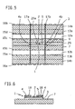
- Fig. 5 illustrates a variant of the embodiment of Fig. 4 in which the only significant difference is provided by an additional liquid resin or prepreg intermediate layer 29 in the stacked layer structure between the base layer 7 and the cover layer 9.
- this intermediate layer 29 is provided with a window region 29a, into which the component 2 protrudes.
- Laminating the structure also liquefies the resin material of the liquid resin or prepreg intermediate layer 29 and contributes to the complete gap-free enclosure of the insert piece 1 together with the assembled component 2 at.
- the intermediate layer 29 with the window 29a provides for receiving space of the chip 2 mounted on the insert piece 1 and thus facilitates homogeneous gap-free embedding of the insert piece between the two liquid resin or prepreg layers 7, 9 covering the bottom or top, without the latter being present Clearly bulge in the area of the insert piece 1.
- the intermediate layer 29 provides a relief of the chip 2 from the mechanical pressure loads acting during the pressing or laminating, which is advantageous, in particular, for relatively thin, pressure-sensitive chips.
- the intermediate layer 29 may also constitute a layer layer of a multilayer cover layer consisting of the cover layer 9 and the interlayer layer 29, in which case at least the intermediate layer 29, which lies on the side of this multilayer cover layer facing the insert piece 1, lies in this multilayer cover layer. is provided with the window 29a.
- the window 29a may extend over the entire area of the insert piece 1 if the latter requires a total of additional receiving space.
- Fig. 6 shows a variant with regard to the design of the insert piece 1.
- a structured height spacer layer 18 over the rewiring support layer 3 and the rewiring 4, 5 in the area outside the mounted chip 2 and with a little lateral distance from this on.
- the application of the height spacer layer 18 can be done before or after placing the insert 1 on the backing layer 7 as needed.
- the height spacer layer 18 extends from the rewiring carrier layer 3 or the rewiring 4, 5 from to at least the top of the assembled chip 2, in the example of Fig. 5 something as shown above.
- the height spacer layer 18 is capable of relieving the chip 2 from excessive compressive stresses in compressing the prepared layer stack in which the insert 1 is integrated.
- an epoxy resin material can be used as the material for the structured height-spacer layer 18 that can be produced, for example, by screen printing technology.
- a cutout in the region of the contact points 4 can be provided, which can be produced in a conventional manner, in order to avoid subsequent via problems or to improve the durability of the pressure contact, eg a copper sleeve.
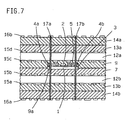
- Fig. 7 illustrates the integration of an insert of the in Fig. 6 shown in a circuit board multilayer structure, which incidentally that of Fig. 4 corresponds, so that reference can be made to the above description.
- the cover layer 9 is provided with a matching recess 9a.
- a corresponding recess may be provided in the base layer 7.
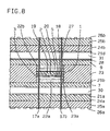
- Fig. 8 illustrates the integration of the insert 1 according to Fig. 6 in another example.
- the example of Fig. 8 includes the insert piece 1 starting from the structure according to Fig. 6
- a filling / planarization layer 19 which extends over the entire surface and with a substantially planar top over the height spacer layer 18 and the chip 2 and thereby also fills the lateral clearance between the chip 2 and the structured height spacer layer 18.
- an insert cover layer 20 is applied over the entire surface, which is identical in material and thickness to the rewiring support layer 3 or alternatively, this corresponds at least largely in thickness and in the thermal expansion behavior.
- the insert cap layer 20 may be e.g. how the rewiring support layer 3 is made of a polyimide material or a ceramic material.
- the insert piece 1 rests on a buffer layer piece 22a which is formed of a material which can compensate for mechanical stresses, in particular due to thermal stresses, or mediate between the thermal expansion coefficients of the upper-side rewiring carrier layer 3 of the insert 1 and an electrically conductive layer adjoining on the underside ,
- the buffer layer piece may consist of an epoxy resin material.
- the buffer layer piece 22a in this example rests on the base layer 7, which in turn lies on an inner layer 30 provided with conductor track structures on both sides.
- the buffer layer piece 22a can be produced, for example, by screen printing or cut out of a corresponding layer material and placed on the relevant layer on the backing layer 7 and fixed.
- the insert piece 1 with the described structure.
- Next includes the layer structure of Fig. 8 above the backing layer 7 a liquid resin or Prepreg intermediate layer 23 with a window portion 23a, in which the insert piece 1 including buffer layer piece 22a is received.
- the window 23a is cut or milled out in the size of the buffer layer piece 22a whose lateral dimension corresponds to that of the insert piece, and the lateral gap to the insert piece 1 then fills with molten resin material during later pressing.
- the buffer layer piece 22a it may be advantageous to provide a corresponding buffer layer piece 22b as part of the insert 1 between the latter and the cover layer 9 in order to compensate for thermal or mechanical loads, as also shown in FIG Fig. 8 shown.
- a corresponding buffer layer piece 22b as part of the insert 1 between the latter and the cover layer 9 in order to compensate for thermal or mechanical loads, as also shown in FIG Fig. 8 shown.
- the symmetrical arrangement of the upper buffer layer piece 22b to the lower buffer layer piece 22a preferably using substantially equal layer thicknesses and the same or thermal expansion similar materials, another contribution to minimizing the force loads on the insert 1 with its chip 2.
- Another is the printed circuit board multilayer construction of Fig. 6 Overall, in turn, with respect to a stack center plane largely symmetrical nature, and the insert 1 with the chip 2 is seen in the stacking direction in the middle region of the multi-layer structure.
- each of the unitarily illustrated liquid resin or prepreg layers which function as a backing layer and cover layer for covering the insert on both sides, ie in this example layers 7 and 9, and / or the intervening intermediate layer, ie in this example the intermediate layer 23, can each be constructed in multiple layers with at least 2 liquid resin or prepreg layer layers.
- the example according to Fig. 8 has in addition to the lower inner layer or semi-finished circuit board 30 and an upper inner layer or upper semi-finished circuit board 31 with overhead Porter Modellebende 21 d.
- Each of the prepregs 24a, 24b and an outer dielectric layer layer 25a, 25b follows downwards or upwards.
- the outer dielectric layer layers 25a, 25b bear on the outside each an outer conductor pattern plane 26a, 26b, for which they can consist of a prepreg material and a resting copper foil.
- the copper foil is firmly bonded to the prepreg material and the resulting copper layer is patterned in the course of common process steps in the corresponding conductor structure plane 26a, 26b.
- the insert piece 1 has a highly thermally conductive layer 27, for example made of Cu, between the filling / planarizing layer 19 and the insert covering layer 20.
- a highly thermally conductive layer 27 for example made of Cu
- an inner conductor structure plane of the upper semifinished product circuit board 31 is replaced by an unstructured, all-surface heat-conducting layer 28, which may simply be an unstructured copper coating of this semifinished product circuit board 9a, for example.
- vias 17a, 17b additionally a heat transport function by being made of a good thermal conductivity material, such as Cu. Because of the vias 17a, 17b are the associated rewiring contact points and especially the heat conduction layer 27 of the insert 1 with the whole-surface heat-conducting layer 28 of the layer stack in heat-conducting connection, so that very effectively heat, which is formed in the region of the chip 2, via the rewiring 4th 5, on the one hand, and the filling / planarizing layer 19 and the insert heat conducting layer 27, on the other hand, are conducted to the through contacts 17a, 17b and can be dissipated via this to the heat-conducting layer 28 over the entire surface and distributed therefrom.
- a good thermal conductivity material such as Cu.
- This heat dissipation measure can significantly increase the reliability of the function of the chip 2 mounted on the embedded insert 1 and the remaining insert components, especially in cases where appreciable heat generation of components of the insert 1 during operation is caused. It is self-evident that, for the heat-conducting connection to the heat-conducting layer 28 of the layer stack, in each case potential-identical through-contacts are suitable, such as common ground or voltage supply through contacts.
- the insert heat-conducting layer 27 may, for example, already pre-fabricated on the insert top layer 20 of polyimide or the like Layer be made of copper, for example.
- the insert cover layer 20 can be cut out together with the heat-conductive coating 27 of a larger-area layer material and placed with the coating 27 on the filling / planarization layer 19. This can be done as needed before positioning the insert 1 on the backing layer 7 or thereafter.
- the through contacts 17a, 17b without contact with the material of the rewiring carrier layer 3, e.g. Polyimide, pass through it.
- the material of the rewiring carrier layer 3 e.g. Polyimide
- bores are then introduced into the rewiring carrier layer 3 before the embedding of the insert piece 1 between the underlay layer 7 and the cover layer 9 with a larger diameter compared to the later through contacts.
- these holes fill with flowing in resin material from the adjacent resin layer layer.
- the through holes of smaller diameter introduced therethrough after pressing the layer stack can then extend completely within the resin filling at the level of the rewiring carrier layer 3, so that an insulating resin material ring remains between the introduced through contact material and the material of the rewiring carrier layer 3.
- Fig. 9 shows as a further embodiment of the invention a variant of the example of Fig. 5 in which a window area 32a is additionally provided in an inner layer 32 as the sole significant difference for receiving the insert piece 1, on which in this example a comparatively thick, eg, housed, chip 2 or another cased or, for other reasons, relatively thick electrical component is mounted is.
- this inner layer 32 is located in the interior of a multilayer intermediate layer between the backing layer 7, on which the insert piece 1 rests, and the cover layer layer 9.
- the intermediate layer here contains the liquid resin or prepreg intermediate layer 29 as a lower layer layer, the inner layer 32 as a middle layer layer and an upper liquid resin or prepreg layer layer 29b.
- the window 29a of the lower intermediate layer 29 and the window 32a of the inner layer 32 together form a receiving space.
- the upper interlayer ply 29b provides for the upper resin coverage of the insert 1 with the chip 2.
- the insert piece with the chip 2 is embedded on all sides without gaps in surrounding resin material, which in this case comes from the underlay layer 7, the lower interlayer ply 29 and the upper interlayer ply 29b and any gaps especially between the relatively thick chip 2 and the laterally adjacent window edge regions the lower intermediate layer layer 29 and the inner layer 32 fills by liquefying during compression or lamination of the structure and filled corresponding spaces.
- the windows can be provided with lateral dimensions which are at least approximately those of the rest of the insert piece 1, ie in particular of the below the chip 2 layer structure with the redistribution carrier layer 3 in order to also accommodate this part of the insert 1 in a window area, if required.
- This is expedient in particular in the case of a higher insert piece layer structure, as for example in the case of insert pieces of the type described in US Pat Fig. 8 shown, especially if this is still relatively thick mounted components such as the chip 2 of Fig. 9 includes.
- the invention also comprises printed circuit board multi-layer structures, in which an insert with several provided on him, active and / or passive electrical components and / or multiple inserts with one or more electrical components in the interior of the layer stack are integrated.
- a plurality of inserts may be positioned side by side in the same stacking plane with lateral spacing.
- a plurality of insert pieces may be positioned one above the other in the stacking direction in different stacking planes with or without lateral offset.
- the invention enables a very advantageous integration of one or more insert pieces, each having one or more passive and / or active electrical components on a rewiring support layer into the interior of a printed circuit board multilayer structure, wherein the insert piece and in particular its rewiring support layer completely and is embedded gap-free in resin material between a pad and a cover layer, for example, prepreg resin material.
- the structure of the insert and its incorporation into the stack of layers can be realized on request with a high degree of symmetry, which prevents high mechanical stress due to thermal expansion effects at significant temperature changes.
- the rewiring carrier layer of the insert Since the rewiring carrier layer of the insert has a significantly smaller surface area than the embedding layer layers of the printed circuit board layer stack, no delamination problems occur, as might be feared when introducing a continuous rewiring carrier layer, for example made of polyimide.
- a flexible, thin design of the rewiring carrier layer can further contribute to tensile and compressive force stresses occurring due to an interposer effect due to different thermal expansion coefficients of the Compensate involved layer materials.
- a substantially central or symmetrical placement of the component or components on the rewiring carrier layer of the insert also contributes to the reduction of lateral tensile and compressive force loads.
- the printed circuit board multilayer structure according to the invention is relatively easy to produce according to the invention.
- the redistribution substrate layer and the electrical component (s) mounted thereon may be electrically tested prior to crimping the layer stack, which reduces the error rate and improves yield.
- Only electrically functional components are fitted to the redistribution carrier layer, and only functionally assembled insert pieces are laid in the layer stack of the printed circuit board multilayer structure and pressed with this. Due to the segmented introduction of the redistribution only in the portion of the layer stack in which the insert between the dielectric underlayer and the dielectric cover layer is located, can also increase the overall packing density of the printed circuit board multilayer structure.
- the inventive rewiring in the interior of the printed circuit board multilayer structure also space requirements can be reduced to outer layers, and the unbundling of the outer layers simplified, since only corresponding vias are to be led by the rewiring contact points to the surface and the position of the rewiring contact points can be selected in that the associated through-contacts to the outer layers are located at a position which is optimal for the unbundling of the outer layers.
Landscapes
- Engineering & Computer Science (AREA)
- Microelectronics & Electronic Packaging (AREA)
- Production Of Multi-Layered Print Wiring Board (AREA)
- Manufacturing Of Printed Wiring (AREA)
Claims (25)
- Structure multicouches pour carte à circuits, comprenant- un empilement de couches formé de plusieurs couches (7, 9, 10, 11) électriquement isolantes et/ou pourvues de structures de pistes conductrices,
dans laquelle la structure multicouches pour carte à circuits- comprend une pièce en insert (1) à l'intérieur de l'empilement de couches, qui s'étend latéralement uniquement dans une région partielle de l'extension surfacique de l'empilement de couches et qui comprend au moins un composant électrique (2), passif ou actif, monté sur cette pièce, et un fils d'enrobage associé (4, 5), et en ce que- la pièce en insert (1) est noyée sur toute la surface entre deux couches en résine durcie, électriquement isolantes ou diélectriques, qui recouvrent la pièce en insert sur les deux côtés, ladite pièce en insert étant enfermée de tous les côtés sans intervalle par le matériau en résine, et les couches en résine sont formées par des couches en résine liquide durcie ou des couches en préimprégné (7, 9),caractérisée en ce que la pièce en insert est reçue dans des creux respectifs correspondants des deux couches en résine. - Structure multicouches pour carte à circuits selon la revendication 1, caractérisée en outre en ce que l'une au moins des deux couches en résine liquide ou en préimprégné comporte un évidement (9a) dans la région de la pièce en insert ou d'au moins un composant monté sur celle-ci, dans lequel pénètre la pièce en insert ou le composant.
- Structure multicouches pour carte à circuits selon la revendication 1 ou 2, caractérisée en outre en ce qu'il est prévu entre les deux couches en résine liquide ou en préimprégné au moins une couche intermédiaire en résine liquide ou en préimprégné (29), qui comporte une fenêtre (29a) dans la région de la pièce en insert ou d'au moins un composant monté sur celle-ci.
- Structure multicouches pour carte à circuits selon l'une des revendications 1 à 3, caractérisée en outre en ce que l'une au moins des deux couches en résine liquide ou en préimprégné qui recouvre la pièce en insert, et/ou la couche intermédiaire en résine liquide ou en préimprégné est/sont formée(s) à plusieurs nappes avec au moins deux nappes en résine liquide ou en préimprégné.
- Structure multicouches pour carte à circuits selon l'une des revendications 1 à 4, caractérisée en outre en ce qu'il se trouve entre les deux couches en résine liquide ou en préimprégné (7, 9) qui recouvrent la pièce en insert au moins une couche dotée de structures formant pistes conductrices (32), qui comporte une fenêtre (32a) dans la région de la pièce en insert ou d'au moins un composant monté sur celle-ci.
- Structure multicouches pour carte à circuits selon l'une des revendications 1 à 5, caractérisée en outre en ce que le composant électrique respectif (2) est monté sur un emplacement de montage pour composant d'une couche porteuse (3) pour câblage extérieur, sur laquelle est également prévu le câblage extérieur (4, 5).
- Structure multicouches pour carte à circuits selon la revendication 6, caractérisée en outre en ce que le câblage extérieur (4, 5) est prévu sur le même côté de la couche porteuse (3) pour câblage extérieur que l'emplacement de montage pour composant.
- Structure multicouches pour carte à circuits selon la revendication 6 ou 7, caractérisée en outre en ce qu'il est prévu des deux côtés de la couche porteuse respectivement un câblage extérieur et respectivement au moins un composant électrique passif ou actif (2, 2a, 2b, 2c) monté sur la pièce en insert.
- Structure multicouches pour carte à circuits selon l'une des revendications 6 à 8, caractérisée en outre en ce que la couche porteuse pour câblage extérieur est formée en un matériau flexible pour carte à circuits, en particulier un matériau en polymère à cristaux liquides ou un matériau en polyimide, ou encore un matériau céramique, et comporte dans une région médiane l'emplacement de montage pour le montage dudit au moins un composant électrique et dans une région périphérique des emplacements de contact (4) pour câblage extérieur, ainsi que des pistes conductrices (5) pour câblage extérieur, qui s'étendent entre l'emplacement de montage pour composant et les emplacements de contact (4) pour câblage extérieur.
- Structure multicouches pour carte à circuits selon l'une des revendications 1 à 9, caractérisée en outre en ce qu'il est prévu une pièce respective formant couche tampon entre la pièce en insert et l'une au moins des deux couches en résine liquide ou en préimprégné (7, 9) qui recouvrent la pièce en insert.
- Structure multicouches pour carte à circuits selon l'une des revendications 6 à 10, caractérisée en outre par une structure de maintien d'écartement en hauteur (18) sur la couche porteuse (3) pour câblage extérieur, dans la région latéralement à l'extérieur dudit au moins un composant électrique (2), ladite structure de maintien d'écartement en hauteur (18) s'étendant en direction d'empilement au moins aussi loin que ledit au moins un composant électrique (2).
- Structure multicouches pour carte à circuits selon l'une des revendications 6 à 11, caractérisée en outre en ce que la pièce en insert (1) comprend une couche de remplissage et/ou une couche de planéité, qui s'étend sur toute la surface ou seulement dans la région à l'extérieur du ou des composant(s) électrique(s) (2) au-dessus de la couche porteuse (3) pour câblage extérieur.
- Structure multicouches pour carte à circuits selon la revendication 12, caractérisée en outre en ce que la couche de remplissage et/ou de planéité est en un matériau conducteur de la chaleur et électriquement isolant.
- Structure multicouches pour carte à circuits selon la revendication 13, caractérisée en outre en ce que la pièce en insert comprend une couche conductrice de la chaleur au-dessus de la couche de remplissage et/ou de planéité.
- Structure multicouches pour carte à circuits selon l'une des revendications 12 à 14, caractérisée en outre en ce que la pièce en insert (1) comprend, au-dessus de la couche de remplissage et/ou de planéité ou au-dessus de la couche conductrice de la chaleur, une couche de couverture de type analogue à la couche porteuse (3) pour le câblage extérieur pour ce qui concerne le matériau et/ou la taille.
- Structure multicouches pour carte à circuits selon la revendication 14 ou 15, caractérisée en outre en ce que la couche conductrice de la chaleur est reliée de manière à conduire la chaleur via un ou plusieurs contacts traversants (17a, 17b) avec au moins une couche conductrice de la chaleur, structurée ou sur toute la surface, de l'empilement de couches.
- Structure multicouches pour carte à circuits selon l'une des revendications 9 à 16, caractérisée en outre en ce que l'un au moins des emplacements de contact (4) pour câblage extérieur est relié de manière à conduire la chaleur via un ou plusieurs contacts traversants (17a, 17b) avec au moins une couche conductrice de la chaleur, structurée ou sur toute la surface, de l'empilement de couches.
- Structure multicouches pour carte à circuits selon l'une des revendications 1 à 17, caractérisée en outre en ce que les couches en résine liquide ou en préimprégné (7, 9) qui recouvrent la pièce en insert (1) se trouvent approximativement au milieu dans l'empilement de couches, dans la direction d'empilement.
- Procédé pour la fabrication d'une structure multicouche pour carte à circuits selon l'une des revendications 1 à 18, comprenant les étapes suivantes consistant à :- préparer la pièce en insert (1) avec le composant électrique (2) et le câblage extérieur (4, 5) associé,- agencer la pièce en insert (1) sur une couche d'appui préparée (7) de l'empilement de couches, et agencer lesdites une ou plusieurs autres couches de l'empilement de couches au-dessus de la couche d'appui (7) et de la pièce en insert (1), en choisissant pour la couche d'appui (7) et une couche (9) qui recouvre la pièce en insert (1) sur le côté opposé, une nappe de couche respective en résine liquide ou en préimprégné, et- laminer conjointement et/ou presser la structure globale ainsi préparée, de sorte que le matériau en résine dans les zones des couches en résine liquide ou en préimprégné adjacentes à la pièce en insert devient liquide lors du laminage ou du pressage de la structure et enferme la pièce en insert sans intervalle sur tous les côtés.
- Procédé selon la revendication 19, caractérisé en outre en ce que le composant électrique (2) est monté sur la couche porteuse (3) pour câblage extérieur de la pièce en insert (1) et, avant l'introduction de la pièce en insert (1) dans l'empilement de couches, la couche porteuse (3) pour câblage extérieur est pourvue de perçage qui, lors du processus de laminage/pressage successif, se remplissent de matériau en résine provenant de l'environnement, et on réalise ensuite des contacts traversants (17a, 17b) dans les perçages remplis de résine avec un diamètre plus faible par rapport aux perçages de telle façon qu'il demeure une bague en résine entre le contact traversant respectif et la bordure voisine de la couche porteuse (3) pour câblage extérieur.
- Procédé selon la revendication 19 20, caractérisé en outre en ce que les pistes conductrices du câblage extérieur sont formées en appliquant sur la couche porteuse (3) pour câblage extérieur sur toute la surface une couche formant câblage extérieur électriquement conductrice et on subdivise ensuite la couche formant câblage extérieur en réalisant des fossés de séparation dans les pistes conductrices surfaciques en conservant une proportion surfacique importante de la couche formant câblage extérieur.
- Structure multicouches pour carte à circuits selon l'une des revendications 1 à 18, caractérisée en outre en ce que la structure multicouches pour carte à circuits comporte au moins deux plans de structure conductrice extérieure (16a, 16b), entre lesquels s'étendent des contacts traversants (17a, 17b) qui traversent la totalité de l'empilement de couches et qui mettent simultanément en contact des emplacements de contacts associés (4a, 4b) du câblage extérieur et établissent ainsi une liaison électrique des bornes associées du composant (2) vers l'extérieur.
- Structure multicouches pour carte à circuits selon la revendication 22, caractérisée en outre en ce que la structure multicouches pour carte à circuits comporte au moins un plan intérieur de structure conductrice (15a à 15d), et une mise en contact des différents plans de structure conductrice (15a à 15d, 16a, 16b) ainsi que du composant (2) sur la pièce en insert (1) a lieu via les contacts traversants (17a, 17b).
- Procédé selon la revendication 19, 20 août 21, caractérisé en outre en ce qu'il est prévu au moins deux plans extérieurs de structure conductrice (16a, 16b) et des contacts traversants (17a, 17b), lesdits contacts traversants (17a, 17b) s'étendant entre les deux plans extérieurs de structure conductrice en traversant la totalité de l'empilement de couches, et les contacts traversants (17a, 17b) mettent simultanément en contact des emplacements de contacts associés (4a, 4b) du câblage extérieur et établissent ainsi une liaison électrique des bornes associées du composant (2) vers l'extérieur.
- Procédé selon la revendication 24, caractérisé en outre en ce qu'il est prévu au moins un plan intérieur de structure conductrice (15a à 15d), et une mise en contacts des différents plans de structure conductrice (15a à 15d, 16a, 16b) ainsi que du composant (2) sur la pièce en insert (1) a lieu via les contacts traversants (17a, 17b).
Applications Claiming Priority (2)
| Application Number | Priority Date | Filing Date | Title |
|---|---|---|---|
| DE102005032489A DE102005032489B3 (de) | 2005-07-04 | 2005-07-04 | Leiterplatten-Mehrschichtaufbau mit integriertem elektrischem Bauteil und Herstellungsverfahren |
| PCT/EP2006/006511 WO2007003414A1 (fr) | 2005-07-04 | 2006-07-04 | Structure multicouche de plaquettes ayant un composant electrique integre, et son procede de production |
Publications (2)
| Publication Number | Publication Date |
|---|---|
| EP1900264A1 EP1900264A1 (fr) | 2008-03-19 |
| EP1900264B1 true EP1900264B1 (fr) | 2013-05-01 |
Family
ID=37199107
Family Applications (1)
| Application Number | Title | Priority Date | Filing Date |
|---|---|---|---|
| EP06762396.7A Not-in-force EP1900264B1 (fr) | 2005-07-04 | 2006-07-04 | Structure multicouche de plaquettes ayant un composant electrique integre, et son procede de production |
Country Status (6)
| Country | Link |
|---|---|
| US (1) | US8072768B2 (fr) |
| EP (1) | EP1900264B1 (fr) |
| JP (2) | JP2008545260A (fr) |
| CN (1) | CN101258787B (fr) |
| DE (1) | DE102005032489B3 (fr) |
| WO (1) | WO2007003414A1 (fr) |
Cited By (1)
| Publication number | Priority date | Publication date | Assignee | Title |
|---|---|---|---|---|
| DE102021112814A1 (de) | 2021-05-18 | 2022-11-24 | Unimicron Germany GmbH | Verfahren zur Herstellung einer Leiterplatte und Leiterplatte mit mindestens einem eingebetteten elektronischen Bauteil |
Families Citing this family (52)
| Publication number | Priority date | Publication date | Assignee | Title |
|---|---|---|---|---|
| DE102006008050A1 (de) * | 2006-02-21 | 2007-08-23 | Imi Intelligent Medical Implants Ag | Vorrichtung mit flexiblem Mehrschichtsystem zur Kontaktierung oder Elektrostimulation von lebenden Gewebezellen oder Nerven |
| DE102007044602A1 (de) * | 2007-09-19 | 2009-04-23 | Continental Automotive Gmbh | Multilayer-Leiterplatte und Verwendung einer Multilayer-Leiterplatte |
| KR101611804B1 (ko) | 2007-11-01 | 2016-04-11 | 다이니폰 인사츠 가부시키가이샤 | 부품 내장 배선판, 부품 내장 배선판의 제조 방법 |
| JP5515210B2 (ja) * | 2007-12-13 | 2014-06-11 | 大日本印刷株式会社 | 部品内蔵配線板、部品内蔵配線板の製造方法 |
| KR101551177B1 (ko) | 2009-04-21 | 2015-09-09 | 엘지이노텍 주식회사 | 재배선층을 구비한 부품내장형 인쇄회로기판 및 이의 제조방법 |
| DE202009009087U1 (de) * | 2009-07-01 | 2010-12-09 | Aizo Ag Deutschland | Eingebetteter Sandwich-Hybridschaltkreis |
| US8319334B2 (en) | 2009-08-10 | 2012-11-27 | Infineon Technologies Ag | Embedded laminated device |
| CN102576828B (zh) | 2009-09-01 | 2016-04-20 | 萨普拉斯特研究有限责任公司 | 具有集成薄膜电池的印刷电路板 |
| DE102009041952B4 (de) | 2009-09-17 | 2017-03-30 | Airbus Defence and Space GmbH | Verfahren zur Herstellung eines mehrlagigen Keramiksubstrats und mehrlagiges Keramiksubstrat und dessen Verwendung |
| US8837159B1 (en) | 2009-10-28 | 2014-09-16 | Amazon Technologies, Inc. | Low-profile circuit board assembly |
| DE102009060480A1 (de) | 2009-12-18 | 2011-06-22 | Schweizer Electronic AG, 78713 | Leiterstrukturelement und Verfahren zum Herstellen eines Leiterstrukturelements |
| KR101148104B1 (ko) * | 2010-03-16 | 2012-05-22 | 엘지이노텍 주식회사 | 대면적 기판의 후막 형성방법 및 후막구조, 이를 이용한 백라이트유닛, 액정표시장치 |
| JP5257472B2 (ja) * | 2010-04-02 | 2013-08-07 | 株式会社デンソー | 電子装置 |
| DE102010003927A1 (de) * | 2010-04-13 | 2011-10-13 | Zf Friedrichshafen Ag | Steuermodul |
| JP5826532B2 (ja) * | 2010-07-15 | 2015-12-02 | 新光電気工業株式会社 | 半導体装置及びその製造方法 |
| CN103404240B (zh) | 2011-03-03 | 2017-09-08 | 飞利浦照明控股有限公司 | 电路板组装件 |
| DE102011006356A1 (de) * | 2011-03-29 | 2012-10-04 | Continental Automotive Gmbh | Schaltungsträger mit eingebetteter Schaltungsplatine |
| DE102012013920A1 (de) | 2011-07-14 | 2013-01-17 | Hotoprint Elektronik GmbH & Co. KG | Identifizierbare mehrschichtige Leiterplatte sowie Herstellungsverfahren dazu |
| EP2753468B1 (fr) * | 2011-09-09 | 2017-03-08 | LG Innotek Co., Ltd. | Procédé de fabrication de film épais de substrat de grande surface et film épais, unité de rétroéclairage et dispositif d'affichage à cristaux liquides utilisant celui-ci |
| CN102595786B (zh) * | 2012-02-20 | 2014-08-13 | 电子科技大学 | 一种具有内嵌电容的印制电路板及其制造方法 |
| JP5752741B2 (ja) * | 2012-09-26 | 2015-07-22 | 富士フイルム株式会社 | 多層基板および半導体パッケージ |
| KR102042033B1 (ko) * | 2012-10-30 | 2019-11-08 | 엘지이노텍 주식회사 | 칩 실장형 인쇄회로기판 및 그 제조방법 |
| US9653370B2 (en) * | 2012-11-30 | 2017-05-16 | Infineon Technologies Austria Ag | Systems and methods for embedding devices in printed circuit board structures |
| AU2013203801A1 (en) * | 2012-12-15 | 2014-07-03 | JENKINS III, Arthur L. DR | Multilayered Electromagnetic Assembly |
| US9202782B2 (en) | 2013-01-07 | 2015-12-01 | Intel Corporation | Embedded package in PCB build up |
| US8877558B2 (en) | 2013-02-07 | 2014-11-04 | Harris Corporation | Method for making electronic device with liquid crystal polymer and related devices |
| DE102013102542A1 (de) * | 2013-03-13 | 2014-09-18 | Schweizer Electronic Ag | Elektronisches Bauteil und Verfahren zum Herstellen eines elektronischen Bauteils |
| US9293438B2 (en) | 2013-07-03 | 2016-03-22 | Harris Corporation | Method for making electronic device with cover layer with openings and related devices |
| US9831482B2 (en) | 2013-09-06 | 2017-11-28 | Johnson Controls Technology Company | Battery module lid system and method |
| DE102013015956A1 (de) | 2013-09-25 | 2014-04-10 | Daimler Ag | Leistungsmodul, insbesondere für Kraftfahrzeuge |
| EP2988328B1 (fr) | 2014-08-19 | 2021-05-12 | ABB Schweiz AG | Module semi-conducteur de puissance et procédé de fabrication de celui-ci |
| DE102015113324A1 (de) * | 2015-08-12 | 2017-02-16 | Schweizer Electronic Ag | Leiterstrukturelement mit einlaminiertem Innenlagensubstrat und Verfahren zu dessen Herstellung |
| DE102015113503A1 (de) * | 2015-08-14 | 2017-02-16 | Schweizer Electronic Ag | Elektronisches Schaltelement und modular aufgebauter Stromrichter |
| CN105142362A (zh) * | 2015-08-26 | 2015-12-09 | 昆山苏杭电路板有限公司 | 四层埋置元件印制板加工方法 |
| DE112016003990B4 (de) | 2015-09-02 | 2023-09-07 | At & S Austria Technologie & Systemtechnik Aktiengesellschaft | Elektronisches Gerät mit eingebetteter elektronischer Komponente und Herstellungsverfahren |
| CN106502317B (zh) | 2015-09-03 | 2019-09-27 | 苹果公司 | 电子设备的结构特征件 |
| DE102017200127A1 (de) | 2017-01-05 | 2018-07-05 | Fraunhofer-Gesellschaft zur Förderung der angewandten Forschung e.V. | Modulanordnung mit eingebetteten Komponenten und einer integrierten Antenne, Vorrichtung mit Modulanordnungen und Verfahren zur Herstellung |
| DE102017200126A1 (de) | 2017-01-05 | 2018-07-05 | Fraunhofer-Gesellschaft zur Förderung der angewandten Forschung e.V. | Modulanordnung mit integrierter Antenne und eingebetteten Komponenten sowie Verfahren zur Herstellung einer Modulanordnung |
| DE102017200128A1 (de) | 2017-01-05 | 2018-07-05 | Fraunhofer-Gesellschaft zur Förderung der angewandten Forschung e.V. | Elektronisches Modul mit integrierter Antenne und Verfahren zur Herstellung |
| DE102017221540A1 (de) * | 2017-11-30 | 2019-06-06 | Contitech Elastomer-Beschichtungen Gmbh | Verbundwerkstoff |
| CN111372369B (zh) | 2018-12-25 | 2023-07-07 | 奥特斯科技(重庆)有限公司 | 具有部件屏蔽的部件承载件及其制造方法 |
| CN116207074A (zh) | 2019-07-29 | 2023-06-02 | 群创光电股份有限公司 | 电子装置 |
| US11824013B2 (en) | 2019-08-15 | 2023-11-21 | Intel Corporation | Package substrate with reduced interconnect stress |
| CN111031710B (zh) * | 2019-11-24 | 2024-06-21 | 奥士康科技股份有限公司 | 一种防止内层芯板叠错装置 |
| CN113498633B (zh) * | 2020-01-21 | 2023-09-15 | 鹏鼎控股(深圳)股份有限公司 | 内埋电子元件的电路板及制作方法 |
| DE102020206769B3 (de) * | 2020-05-29 | 2021-06-10 | Fraunhofer-Gesellschaft zur Förderung der angewandten Forschung eingetragener Verein | Mikroelektronische anordnung und verfahren zur herstellung derselben |
| CN112165767B (zh) * | 2020-10-27 | 2021-12-07 | 惠州市特创电子科技股份有限公司 | 多层线路板以及移动通讯装置 |
| DE102021105529A1 (de) | 2021-03-08 | 2022-09-08 | Rogers Germany Gmbh | Leiterplatte, Metall-Keramik-Substrat als Einsatz und Verfahren zur Herstellung eines solchen Einsatzes |
| DE102021118202A1 (de) * | 2021-04-29 | 2022-11-03 | At&S Austria Technologie & Systemtechnik Aktiengesellschaft | Komponententräger mit eingebetteter Komponente, welche mittels eines galvanischen Verbindungsstapels verbunden ist |
| US11924962B2 (en) * | 2021-10-21 | 2024-03-05 | Dell Products L.P. | Printed circuit board (PCB) including heatsinks |
| CN114867204B (zh) * | 2022-05-26 | 2023-11-17 | 深圳市金晟达电子技术有限公司 | 一种加强型高频毫米波混合电路板 |
| CN117316774A (zh) * | 2022-06-20 | 2023-12-29 | 宏启胜精密电子(秦皇岛)有限公司 | 封装结构及其制作方法、显示组件 |
Citations (2)
| Publication number | Priority date | Publication date | Assignee | Title |
|---|---|---|---|---|
| US20030057544A1 (en) * | 2001-09-13 | 2003-03-27 | Nathan Richard J. | Integrated assembly protocol |
| US20040229446A1 (en) * | 2003-05-12 | 2004-11-18 | Shinko Electric Industries Co., Ltd. | Method of production of semiconductor device |
Family Cites Families (30)
| Publication number | Priority date | Publication date | Assignee | Title |
|---|---|---|---|---|
| US3763404A (en) * | 1968-03-01 | 1973-10-02 | Gen Electric | Semiconductor devices and manufacture thereof |
| US4544989A (en) * | 1980-06-30 | 1985-10-01 | Sharp Kabushiki Kaisha | Thin assembly for wiring substrate |
| US5081563A (en) * | 1990-04-27 | 1992-01-14 | International Business Machines Corporation | Multi-layer package incorporating a recessed cavity for a semiconductor chip |
| JP2816028B2 (ja) * | 1991-02-18 | 1998-10-27 | 株式会社東芝 | 半導体装置の製造方法 |
| JP3086332B2 (ja) | 1992-06-08 | 2000-09-11 | 日本シイエムケイ株式会社 | 多層プリント配線板の製造方法 |
| JP3198796B2 (ja) * | 1993-06-25 | 2001-08-13 | 富士電機株式会社 | モールドモジュール |
| US5426263A (en) * | 1993-12-23 | 1995-06-20 | Motorola, Inc. | Electronic assembly having a double-sided leadless component |
| DE4403513A1 (de) * | 1994-02-04 | 1995-08-10 | Giesecke & Devrient Gmbh | Chipkarte mit einem elektronischen Modul und Verfahren zur Herstellung einer solchen Chipkarte |
| DE19528730A1 (de) * | 1995-08-04 | 1997-02-06 | Giesecke & Devrient Gmbh | Verfahren zur Herstellung eines Datenträgers |
| DE19535989C3 (de) * | 1995-09-27 | 2003-03-27 | Siemens Ag | Chipmodul |
| CN1094717C (zh) * | 1995-11-16 | 2002-11-20 | 松下电器产业株式会社 | 印刷电路板的安装体 |
| DE19627543B9 (de) * | 1996-05-18 | 2004-10-14 | Thomas Hofmann | Multi-Layer-Substrat sowie Verfahren zu seiner Herstellung |
| US5970346A (en) * | 1997-09-19 | 1999-10-19 | Taiwan Semiconductor Manufacturing Company, Ltd. | Fuse window guard ring structure for nitride capped self aligned contact processes |
| JP3236818B2 (ja) * | 1998-04-28 | 2001-12-10 | 京セラ株式会社 | 素子内蔵多層配線基板の製造方法 |
| JP3207174B2 (ja) * | 1999-02-01 | 2001-09-10 | 京セラ株式会社 | 電気素子搭載配線基板およびその製造方法 |
| JP2000294922A (ja) * | 1999-04-01 | 2000-10-20 | Victor Co Of Japan Ltd | 多層プリント配線板用の絶縁樹脂組成物 |
| DE19954941C2 (de) * | 1999-11-16 | 2003-11-06 | Fraunhofer Ges Forschung | Verfahren zum Integrieren eines Chips innerhalb einer Leiterplatte |
| JP3673448B2 (ja) * | 2000-05-30 | 2005-07-20 | 京セラ株式会社 | コンデンサ素子内蔵配線基板 |
| US6538210B2 (en) * | 1999-12-20 | 2003-03-25 | Matsushita Electric Industrial Co., Ltd. | Circuit component built-in module, radio device having the same, and method for producing the same |
| JP3478281B2 (ja) * | 2001-06-07 | 2003-12-15 | ソニー株式会社 | Icカード |
| JP2003243797A (ja) * | 2002-02-19 | 2003-08-29 | Matsushita Electric Ind Co Ltd | モジュール部品 |
| EP1351301B1 (fr) * | 2002-04-03 | 2009-06-17 | Panasonic Corporation | Module semi-conducteur intégré fonctionnant en bande millimétrique |
| US6818469B2 (en) * | 2002-05-27 | 2004-11-16 | Nec Corporation | Thin film capacitor, method for manufacturing the same and printed circuit board incorporating the same |
| JP2004158545A (ja) * | 2002-11-05 | 2004-06-03 | Denso Corp | 多層基板及びその製造方法 |
| JP2004228397A (ja) * | 2003-01-24 | 2004-08-12 | Cmk Corp | 積層チップコンデンサを内蔵した多層プリント配線板の製造方法 |
| US7180169B2 (en) * | 2003-08-28 | 2007-02-20 | Matsushita Electric Industrial Co., Ltd. | Circuit component built-in module and method for manufacturing the same |
| US7488895B2 (en) * | 2003-09-29 | 2009-02-10 | Panasonic Corporation | Method for manufacturing component built-in module, and component built-in module |
| US7489032B2 (en) * | 2003-12-25 | 2009-02-10 | Casio Computer Co., Ltd. | Semiconductor device including a hard sheet to reduce warping of a base plate and method of fabricating the same |
| JP2005234683A (ja) * | 2004-02-17 | 2005-09-02 | Matsushita Electric Ind Co Ltd | Icカード |
| JP2006041122A (ja) * | 2004-07-26 | 2006-02-09 | Shinko Electric Ind Co Ltd | 電子部品内蔵要素、電子装置及びそれらの製造方法 |
-
2005
- 2005-07-04 DE DE102005032489A patent/DE102005032489B3/de not_active Expired - Fee Related
-
2006
- 2006-07-04 US US11/988,289 patent/US8072768B2/en not_active Expired - Fee Related
- 2006-07-04 CN CN2006800323285A patent/CN101258787B/zh not_active Expired - Fee Related
- 2006-07-04 JP JP2008518758A patent/JP2008545260A/ja not_active Withdrawn
- 2006-07-04 WO PCT/EP2006/006511 patent/WO2007003414A1/fr not_active Ceased
- 2006-07-04 EP EP06762396.7A patent/EP1900264B1/fr not_active Not-in-force
-
2012
- 2012-07-23 JP JP2012162648A patent/JP2012238874A/ja not_active Withdrawn
Patent Citations (2)
| Publication number | Priority date | Publication date | Assignee | Title |
|---|---|---|---|---|
| US20030057544A1 (en) * | 2001-09-13 | 2003-03-27 | Nathan Richard J. | Integrated assembly protocol |
| US20040229446A1 (en) * | 2003-05-12 | 2004-11-18 | Shinko Electric Industries Co., Ltd. | Method of production of semiconductor device |
Cited By (2)
| Publication number | Priority date | Publication date | Assignee | Title |
|---|---|---|---|---|
| DE102021112814A1 (de) | 2021-05-18 | 2022-11-24 | Unimicron Germany GmbH | Verfahren zur Herstellung einer Leiterplatte und Leiterplatte mit mindestens einem eingebetteten elektronischen Bauteil |
| US12342466B2 (en) | 2021-05-18 | 2025-06-24 | Unimicron Germany GmbH | Method for producing a printed circuit board, and printed circuit board having at least one embedded electronic component |
Also Published As
| Publication number | Publication date |
|---|---|
| JP2012238874A (ja) | 2012-12-06 |
| CN101258787A (zh) | 2008-09-03 |
| US20090041994A1 (en) | 2009-02-12 |
| CN101258787B (zh) | 2011-02-09 |
| WO2007003414A1 (fr) | 2007-01-11 |
| DE102005032489B3 (de) | 2006-11-16 |
| JP2008545260A (ja) | 2008-12-11 |
| EP1900264A1 (fr) | 2008-03-19 |
| US8072768B2 (en) | 2011-12-06 |
Similar Documents
| Publication | Publication Date | Title |
|---|---|---|
| EP1900264B1 (fr) | Structure multicouche de plaquettes ayant un composant electrique integre, et son procede de production | |
| DE112004001727B4 (de) | Verfahren zur Herstellung eines elektronischen Moduls | |
| DE102011006489B4 (de) | Leiterplatte mit eingebautem Halbleiterchip und Verfahren zur Herstellung derselben | |
| DE102005026098B3 (de) | Nutzen und Halbleiterbauteil aus einer Verbundplatte mit Halbleiterchips und Kunststoffgehäusemasse sowie Verfahren zur Herstellung derselben | |
| DE102010042567B3 (de) | Verfahren zum Herstellen eines Chip-Package und Chip-Package | |
| DE69428181T2 (de) | Vorrichtung mit Chipgehäuse und Verfahren zu Ihrer Herstellung | |
| EP2524394B1 (fr) | Composant électronique, procédé pour sa fabrication et plaquette de circuits imprimés comportant un composant électronique | |
| DE602004009821T2 (de) | Halbleiterbauelement und Herstellungsverfahren dafür | |
| DE69711735T2 (de) | Gedruckte Schaltungsplatte oder Halbleitervorrichtung mit anisotrop leitenden Platten | |
| DE102014109909B4 (de) | Chipbaugruppe mit eingebetteter passiver Komponente und Verfahren zur Herstellung | |
| DE10259221B4 (de) | Elektronisches Bauteil mit einem Stapel aus Halbleiterchips und Verfahren zur Herstellung desselben | |
| DE10352946B4 (de) | Halbleiterbauteil mit Halbleiterchip und Umverdrahtungslage sowie Verfahren zur Herstellung desselben | |
| DE10045043B4 (de) | Halbleiterbauteil und Verfahren zu dessen Herstellung | |
| DE112008003532T5 (de) | Verfahren zum Herstellen eines Mehrschichtverdrahtungssubstrats | |
| JP4024188B2 (ja) | 半導体チップ内蔵配線板の製造方法 | |
| DE60032067T2 (de) | Mehrschichtige Leiterplatte und Verfahren zu deren Herstellung | |
| DE19930308A1 (de) | Multichipmodul mit Silicium-Trägersubstrat | |
| DE102013203919B4 (de) | Halbleitergehäuse und Verfahren zu ihrer Herstellung | |
| DE10240461A1 (de) | Universelles Gehäuse für ein elektronisches Bauteil mit Halbleiterchip und Verfahren zu seiner Herstellung | |
| DE10228593A1 (de) | Elektronisches Bauteil mit einer Gehäusepackung | |
| WO2013013964A1 (fr) | Dispositif support, dispositif électrique pourvu d'un dispositif support, et procédé de fabrication de ces dispositifs | |
| DE102005043557A1 (de) | Halbleiterbauteil mit Durchkontakten zwischen Oberseite und Rückseite und Verfahren zur Herstellung desselben | |
| DE102011007842A1 (de) | Mehrschichtige Leiterplatte | |
| WO2011003647A1 (fr) | Carte de circuits | |
| DE102005003125A1 (de) | Elektrische Schaltung und Verfahren zur Herstellung einer elektrischen Schaltung |
Legal Events
| Date | Code | Title | Description |
|---|---|---|---|
| PUAI | Public reference made under article 153(3) epc to a published international application that has entered the european phase |
Free format text: ORIGINAL CODE: 0009012 |
|
| 17P | Request for examination filed |
Effective date: 20071220 |
|
| AK | Designated contracting states |
Kind code of ref document: A1 Designated state(s): AT BE BG CH CY CZ DE DK EE ES FI FR GB GR HU IE IS IT LI LT LU LV MC NL PL PT RO SE SI SK TR |
|
| DAX | Request for extension of the european patent (deleted) | ||
| RIN1 | Information on inventor provided before grant (corrected) |
Inventor name: GOTTWALD, THOMAS Inventor name: OCKENFUSS, ULRICH |
|
| 17Q | First examination report despatched |
Effective date: 20100216 |
|
| DAX | Request for extension of the european patent (deleted) | ||
| GRAP | Despatch of communication of intention to grant a patent |
Free format text: ORIGINAL CODE: EPIDOSNIGR1 |
|
| GRAS | Grant fee paid |
Free format text: ORIGINAL CODE: EPIDOSNIGR3 |
|
| GRAA | (expected) grant |
Free format text: ORIGINAL CODE: 0009210 |
|
| AK | Designated contracting states |
Kind code of ref document: B1 Designated state(s): AT BE BG CH CY CZ DE DK EE ES FI FR GB GR HU IE IS IT LI LT LU LV MC NL PL PT RO SE SI SK TR |
|
| REG | Reference to a national code |
Ref country code: GB Ref legal event code: FG4D Free format text: NOT ENGLISH |
|
| REG | Reference to a national code |
Ref country code: CH Ref legal event code: EP Ref country code: AT Ref legal event code: REF Ref document number: 610601 Country of ref document: AT Kind code of ref document: T Effective date: 20130515 |
|
| REG | Reference to a national code |
Ref country code: IE Ref legal event code: FG4D Free format text: LANGUAGE OF EP DOCUMENT: GERMAN |
|
| REG | Reference to a national code |
Ref country code: DE Ref legal event code: R096 Ref document number: 502006012794 Country of ref document: DE Effective date: 20130627 |
|
| REG | Reference to a national code |
Ref country code: CH Ref legal event code: NV Representative=s name: BRAUNPAT BRAUN EDER AG, CH |
|
| REG | Reference to a national code |
Ref country code: SE Ref legal event code: TRGR |
|
| REG | Reference to a national code |
Ref country code: NL Ref legal event code: VDEP Effective date: 20130501 |
|
| REG | Reference to a national code |
Ref country code: LT Ref legal event code: MG4D |
|
| PG25 | Lapsed in a contracting state [announced via postgrant information from national office to epo] |
Ref country code: PT Free format text: LAPSE BECAUSE OF FAILURE TO SUBMIT A TRANSLATION OF THE DESCRIPTION OR TO PAY THE FEE WITHIN THE PRESCRIBED TIME-LIMIT Effective date: 20130902 Ref country code: IS Free format text: LAPSE BECAUSE OF FAILURE TO SUBMIT A TRANSLATION OF THE DESCRIPTION OR TO PAY THE FEE WITHIN THE PRESCRIBED TIME-LIMIT Effective date: 20130901 Ref country code: FI Free format text: LAPSE BECAUSE OF FAILURE TO SUBMIT A TRANSLATION OF THE DESCRIPTION OR TO PAY THE FEE WITHIN THE PRESCRIBED TIME-LIMIT Effective date: 20130501 Ref country code: LT Free format text: LAPSE BECAUSE OF FAILURE TO SUBMIT A TRANSLATION OF THE DESCRIPTION OR TO PAY THE FEE WITHIN THE PRESCRIBED TIME-LIMIT Effective date: 20130501 Ref country code: ES Free format text: LAPSE BECAUSE OF FAILURE TO SUBMIT A TRANSLATION OF THE DESCRIPTION OR TO PAY THE FEE WITHIN THE PRESCRIBED TIME-LIMIT Effective date: 20130812 Ref country code: GR Free format text: LAPSE BECAUSE OF FAILURE TO SUBMIT A TRANSLATION OF THE DESCRIPTION OR TO PAY THE FEE WITHIN THE PRESCRIBED TIME-LIMIT Effective date: 20130802 Ref country code: SI Free format text: LAPSE BECAUSE OF FAILURE TO SUBMIT A TRANSLATION OF THE DESCRIPTION OR TO PAY THE FEE WITHIN THE PRESCRIBED TIME-LIMIT Effective date: 20130501 |
|
| PG25 | Lapsed in a contracting state [announced via postgrant information from national office to epo] |
Ref country code: PL Free format text: LAPSE BECAUSE OF FAILURE TO SUBMIT A TRANSLATION OF THE DESCRIPTION OR TO PAY THE FEE WITHIN THE PRESCRIBED TIME-LIMIT Effective date: 20130501 Ref country code: BG Free format text: LAPSE BECAUSE OF FAILURE TO SUBMIT A TRANSLATION OF THE DESCRIPTION OR TO PAY THE FEE WITHIN THE PRESCRIBED TIME-LIMIT Effective date: 20130801 Ref country code: CY Free format text: LAPSE BECAUSE OF FAILURE TO SUBMIT A TRANSLATION OF THE DESCRIPTION OR TO PAY THE FEE WITHIN THE PRESCRIBED TIME-LIMIT Effective date: 20130501 |
|
| PG25 | Lapsed in a contracting state [announced via postgrant information from national office to epo] |
Ref country code: LV Free format text: LAPSE BECAUSE OF FAILURE TO SUBMIT A TRANSLATION OF THE DESCRIPTION OR TO PAY THE FEE WITHIN THE PRESCRIBED TIME-LIMIT Effective date: 20130501 |
|
| BERE | Be: lapsed |
Owner name: SCHWEIZER ELECTRONIC A.G. Effective date: 20130731 |
|
| PG25 | Lapsed in a contracting state [announced via postgrant information from national office to epo] |
Ref country code: DK Free format text: LAPSE BECAUSE OF FAILURE TO SUBMIT A TRANSLATION OF THE DESCRIPTION OR TO PAY THE FEE WITHIN THE PRESCRIBED TIME-LIMIT Effective date: 20130501 Ref country code: CZ Free format text: LAPSE BECAUSE OF FAILURE TO SUBMIT A TRANSLATION OF THE DESCRIPTION OR TO PAY THE FEE WITHIN THE PRESCRIBED TIME-LIMIT Effective date: 20130501 Ref country code: SK Free format text: LAPSE BECAUSE OF FAILURE TO SUBMIT A TRANSLATION OF THE DESCRIPTION OR TO PAY THE FEE WITHIN THE PRESCRIBED TIME-LIMIT Effective date: 20130501 Ref country code: EE Free format text: LAPSE BECAUSE OF FAILURE TO SUBMIT A TRANSLATION OF THE DESCRIPTION OR TO PAY THE FEE WITHIN THE PRESCRIBED TIME-LIMIT Effective date: 20130501 |
|
| PG25 | Lapsed in a contracting state [announced via postgrant information from national office to epo] |
Ref country code: RO Free format text: LAPSE BECAUSE OF FAILURE TO SUBMIT A TRANSLATION OF THE DESCRIPTION OR TO PAY THE FEE WITHIN THE PRESCRIBED TIME-LIMIT Effective date: 20130501 Ref country code: NL Free format text: LAPSE BECAUSE OF FAILURE TO SUBMIT A TRANSLATION OF THE DESCRIPTION OR TO PAY THE FEE WITHIN THE PRESCRIBED TIME-LIMIT Effective date: 20130501 Ref country code: MC Free format text: LAPSE BECAUSE OF FAILURE TO SUBMIT A TRANSLATION OF THE DESCRIPTION OR TO PAY THE FEE WITHIN THE PRESCRIBED TIME-LIMIT Effective date: 20130501 Ref country code: IT Free format text: LAPSE BECAUSE OF FAILURE TO SUBMIT A TRANSLATION OF THE DESCRIPTION OR TO PAY THE FEE WITHIN THE PRESCRIBED TIME-LIMIT Effective date: 20130501 |
|
| PLBE | No opposition filed within time limit |
Free format text: ORIGINAL CODE: 0009261 |
|
| STAA | Information on the status of an ep patent application or granted ep patent |
Free format text: STATUS: NO OPPOSITION FILED WITHIN TIME LIMIT |
|
| 26N | No opposition filed |
Effective date: 20140204 |
|
| GBPC | Gb: european patent ceased through non-payment of renewal fee |
Effective date: 20130801 |
|
| REG | Reference to a national code |
Ref country code: IE Ref legal event code: MM4A |
|
| PG25 | Lapsed in a contracting state [announced via postgrant information from national office to epo] |
Ref country code: BE Free format text: LAPSE BECAUSE OF NON-PAYMENT OF DUE FEES Effective date: 20130731 |
|
| REG | Reference to a national code |
Ref country code: DE Ref legal event code: R097 Ref document number: 502006012794 Country of ref document: DE Effective date: 20140204 |
|
| PG25 | Lapsed in a contracting state [announced via postgrant information from national office to epo] |
Ref country code: IE Free format text: LAPSE BECAUSE OF NON-PAYMENT OF DUE FEES Effective date: 20130704 Ref country code: GB Free format text: LAPSE BECAUSE OF NON-PAYMENT OF DUE FEES Effective date: 20130801 |
|
| PG25 | Lapsed in a contracting state [announced via postgrant information from national office to epo] |
Ref country code: TR Free format text: LAPSE BECAUSE OF FAILURE TO SUBMIT A TRANSLATION OF THE DESCRIPTION OR TO PAY THE FEE WITHIN THE PRESCRIBED TIME-LIMIT Effective date: 20130501 |
|
| REG | Reference to a national code |
Ref country code: FR Ref legal event code: PLFP Year of fee payment: 10 |
|
| PG25 | Lapsed in a contracting state [announced via postgrant information from national office to epo] |
Ref country code: HU Free format text: LAPSE BECAUSE OF FAILURE TO SUBMIT A TRANSLATION OF THE DESCRIPTION OR TO PAY THE FEE WITHIN THE PRESCRIBED TIME-LIMIT; INVALID AB INITIO Effective date: 20060704 Ref country code: LU Free format text: LAPSE BECAUSE OF NON-PAYMENT OF DUE FEES Effective date: 20130704 |
|
| REG | Reference to a national code |
Ref country code: FR Ref legal event code: PLFP Year of fee payment: 11 |
|
| REG | Reference to a national code |
Ref country code: DE Ref legal event code: R082 Ref document number: 502006012794 Country of ref document: DE Representative=s name: GLAWE DELFS MOLL PARTNERSCHAFT MBB VON PATENT-, DE |
|
| REG | Reference to a national code |
Ref country code: FR Ref legal event code: PLFP Year of fee payment: 12 |
|
| REG | Reference to a national code |
Ref country code: CH Ref legal event code: PCAR Free format text: NEW ADDRESS: HOLEESTRASSE 87, 4054 BASEL (CH) |
|
| REG | Reference to a national code |
Ref country code: FR Ref legal event code: PLFP Year of fee payment: 13 |
|
| PGFP | Annual fee paid to national office [announced via postgrant information from national office to epo] |
Ref country code: DE Payment date: 20180921 Year of fee payment: 13 Ref country code: FR Payment date: 20180723 Year of fee payment: 13 |
|
| PGFP | Annual fee paid to national office [announced via postgrant information from national office to epo] |
Ref country code: AT Payment date: 20180719 Year of fee payment: 13 Ref country code: CH Payment date: 20180725 Year of fee payment: 13 Ref country code: SE Payment date: 20180725 Year of fee payment: 13 |
|
| REG | Reference to a national code |
Ref country code: DE Ref legal event code: R119 Ref document number: 502006012794 Country of ref document: DE |
|
| REG | Reference to a national code |
Ref country code: CH Ref legal event code: PL |
|
| REG | Reference to a national code |
Ref country code: SE Ref legal event code: EUG |
|
| REG | Reference to a national code |
Ref country code: AT Ref legal event code: MM01 Ref document number: 610601 Country of ref document: AT Kind code of ref document: T Effective date: 20190704 |
|
| PG25 | Lapsed in a contracting state [announced via postgrant information from national office to epo] |
Ref country code: DE Free format text: LAPSE BECAUSE OF NON-PAYMENT OF DUE FEES Effective date: 20200201 Ref country code: AT Free format text: LAPSE BECAUSE OF NON-PAYMENT OF DUE FEES Effective date: 20190704 Ref country code: SE Free format text: LAPSE BECAUSE OF NON-PAYMENT OF DUE FEES Effective date: 20190705 |
|
| PG25 | Lapsed in a contracting state [announced via postgrant information from national office to epo] |
Ref country code: CH Free format text: LAPSE BECAUSE OF NON-PAYMENT OF DUE FEES Effective date: 20190731 Ref country code: LI Free format text: LAPSE BECAUSE OF NON-PAYMENT OF DUE FEES Effective date: 20190731 |
|
| PG25 | Lapsed in a contracting state [announced via postgrant information from national office to epo] |
Ref country code: FR Free format text: LAPSE BECAUSE OF NON-PAYMENT OF DUE FEES Effective date: 20190731 |