EP1901428A1 - Übertragung von digitalen Daten mit Hilfe eines Transformators - Google Patents
Übertragung von digitalen Daten mit Hilfe eines Transformators Download PDFInfo
- Publication number
- EP1901428A1 EP1901428A1 EP07115966A EP07115966A EP1901428A1 EP 1901428 A1 EP1901428 A1 EP 1901428A1 EP 07115966 A EP07115966 A EP 07115966A EP 07115966 A EP07115966 A EP 07115966A EP 1901428 A1 EP1901428 A1 EP 1901428A1
- Authority
- EP
- European Patent Office
- Prior art keywords
- transformer
- signal
- digital signal
- pulses
- rising
- Prior art date
- Legal status (The legal status is an assumption and is not a legal conclusion. Google has not performed a legal analysis and makes no representation as to the accuracy of the status listed.)
- Withdrawn
Links
Images


Classifications
-
- H—ELECTRICITY
- H01—ELECTRIC ELEMENTS
- H01F—MAGNETS; INDUCTANCES; TRANSFORMERS; SELECTION OF MATERIALS FOR THEIR MAGNETIC PROPERTIES
- H01F19/00—Fixed transformers or mutual inductances of the signal type
- H01F19/04—Transformers or mutual inductances suitable for handling frequencies considerably beyond the audio range
- H01F19/08—Transformers having magnetic bias, e.g. for handling pulses
-
- H—ELECTRICITY
- H03—ELECTRONIC CIRCUITRY
- H03K—PULSE TECHNIQUE
- H03K5/00—Manipulating of pulses not covered by one of the other main groups of this subclass
- H03K5/125—Discriminating pulses
- H03K5/1252—Suppression or limitation of noise or interference
-
- H—ELECTRICITY
- H03—ELECTRONIC CIRCUITRY
- H03K—PULSE TECHNIQUE
- H03K5/00—Manipulating of pulses not covered by one of the other main groups of this subclass
- H03K5/153—Arrangements in which a pulse is delivered at the instant when a predetermined characteristic of an input signal is present or at a fixed time interval after this instant
- H03K5/1534—Transition or edge detectors
-
- H—ELECTRICITY
- H04—ELECTRIC COMMUNICATION TECHNIQUE
- H04L—TRANSMISSION OF DIGITAL INFORMATION, e.g. TELEGRAPHIC COMMUNICATION
- H04L25/00—Baseband systems
- H04L25/02—Details ; arrangements for supplying electrical power along data transmission lines
- H04L25/0264—Arrangements for coupling to transmission lines
- H04L25/0266—Arrangements for providing Galvanic isolation, e.g. by means of magnetic or capacitive coupling
-
- H—ELECTRICITY
- H01—ELECTRIC ELEMENTS
- H01F—MAGNETS; INDUCTANCES; TRANSFORMERS; SELECTION OF MATERIALS FOR THEIR MAGNETIC PROPERTIES
- H01F19/00—Fixed transformers or mutual inductances of the signal type
- H01F19/04—Transformers or mutual inductances suitable for handling frequencies considerably beyond the audio range
- H01F19/08—Transformers having magnetic bias, e.g. for handling pulses
- H01F2019/085—Transformer for galvanic isolation
Definitions
- the present invention generally relates to galvanic isolation barriers and, more particularly, the transmission of digital signals through an isolation barrier.
- FIG. 1 very schematically shows in the form of blocks an example of an isolation system or isolator 1 (ISOL) of the type to which the present invention applies.
- This isolator receives, on an input terminal IN, a digital signal Vin having for amplitude a first voltage V1 referenced with respect to a first ground M1, and on an output terminal OUT, a digital signal Vout having for amplitude a second voltage V2 referenced with respect to a second mass M2.
- the amplitudes V1 and V2 may be different or identical.
- opto-couplers To obtain galvanic isolation, opto-couplers, capacitive couplers or transformers are generally used.
- the present invention is more particularly applicable to transformer-based isolation.
- FIG. 2 represents a first known example of a transformer 11.
- a primary winding 11p of the transformer receives, on a first end 12, the signal Vin to be converted and has its second end 13 connected to the ground M1.
- a secondary winding 11s of the transformer has a first end 14 defining the terminal OUT while a second end 15 is connected to the ground M2.
- a current-voltage conversion resistor R across which the signal Vout is taken connects the output terminals 14 and 15.
- FIGS. 3A, 3B and 3C illustrate the operation of the transformer of FIG. 2 for the transmission of a digital signal Vin (for example, a clock signal).
- FIG. 3A represents an example of the appearance of the signal Vin.
- FIG. 3B illustrates the shape of the current Ip in the primary 11p of the transformer.
- Figure 3C illustrates the shape of the current Is in the secondary 11s.
- the rising edges of the signal Vin result in pulses in a first direction (for example positive with the orientations taken in the figures) on the current Is.
- the falling edges result in pulses in the opposite direction. From the current Is, a suitable decoder is able to reconstruct the clock signal having passed through the isolation barrier.
- Figure 4 shows a first example of a solution to avoid this unnecessary consumption.
- the input terminal IN of the insulator is sent to the input of two coding circuits 21 (PCODE) and 22 (NCODE) respectively providing pulses on the rising edges and on the falling edges of the Vin signal.
- the outputs of the circuits 21 and 22 are connected to respective first ends 12 and 12 'of the primary of the transformers 11 and 11' whose second respective ends 13 and 13 'are connected to the ground M1.
- DECODE decoding circuit 23
- a disadvantage of the insulator of Figure 4 is that it requires two transformers, which increases the size and cost.
- Figure 5 shows a second example of a solution to avoid excessive consumption of the transformer.
- a coding circuit 21 '(CODE) of the digital signal Vin to be processed supplies, at the primary 11p of a transformer 11, a pulse for the rising edges and a sequence of two close pulses for the falling edges.
- a decoding circuit 23 '(DECODE) operates, on the secondary side, fronts and pairs of fronts to reconstitute the signal Vout.
- a disadvantage of the isolator of FIG. 5 is that it requires, on the decoding side, a determined observation window in order to be able to distinguish the rising edges from the pairs of falling edges which are translated at the secondary level by pulses in the same direction. .
- the frequency of the digital signal that can be processed, and thus the bandwidth of the system, is thus limited.
- the present invention aims to overcome all or part of the disadvantages of known transformers for transferring digital signals through an isolation barrier.
- the invention is more particularly a solution requiring only one transformer.
- the invention also aims at a solution exploiting simplified coding and decoding circuits.
- the invention is also aimed at a solution with a large bandwidth.
- the present invention provides a method of transferring a digital signal through a transformer, wherein the current in a primary winding of the transformer is inverted along the rising or falling edge of the digital signal to be transferred.
- the digital signal to be transferred is coded to generate pulses on each of its fronts.
- respective rising and falling edges of an output signal are generated in the direction of the current in a secondary winding of the transformer.
- the respective outputs of the first and third inverters are connected to a positive supply line by capacitors.
- the decoding circuit comprises two comparators whose outputs are connected to respective inputs for setting and resetting a flip-flop whose output provides the digital signal transferred.
- FIG. 6 very schematically shows in the form of blocks an embodiment of a system for transferring digital signals through an isolation barrier according to the present invention.
- An input terminal IN receiving a digital Vin signal to be transmitted downstream of the isolation barrier is connected to the inputs of two encoders 31 (PCODE) and 32 (NCODE) providing amplitude pulses V1, referenced to a first mass. (or reference potential) M1, respectively on the rising and falling edges of the digital input signal.
- the circuits 31 and 32 control two selectors S1 and S2 for connection on command of the respective ends 12 and 13 of a primary winding 11p of a transformer 11, either at a positive supply level, or at ground M1.
- the selector S1 selects the voltage V1 in the presence of a pulse representing a rising edge of the input signal and the mass M1 otherwise.
- the selector S2 selects the voltage V1 in the presence of a pulse representing a falling edge of the signal Vin and the mass M1 otherwise.
- the direction of the current Ip in the primary 11p of the transformer 11 is reversed according to the direction of the edge present on the input signal Vin even though the circuits 31 and 32 both provide pulses in the same direction (for example positive ) when they detect a rising or falling edge, respectively.
- a decode circuit 33 (DECODE) provides an output signal on a terminal OUT representing the digital input signal.
- the decoder 33 regenerates the digital signal by exploiting the respective directions of the pulses present on the current Is of the secondary winding 11s.
- FIG. 7 shows an exemplary embodiment of the input circuit of the system of FIG. 6, based on the use of inverters (for example, CMOS inverters).
- the circuit 31 consists of an inverter 71 (INV) powered by the voltage V1.
- the input of the inverter (common grids of the P and N channel transistors in series between the supply lines V1 and M1) is connected to the input terminal IN.
- the output of the inverter is connected to the supply line V1 by a capacitor C72 setting a delay in the switching of the inverter (and therefore the duration of the positive pulses on the rising edges).
- the output of the inverter 71 is connected to a first input of an AND-type logic gate 73 (AND) whose second input receives the signal IN.
- the door 73 defines in a way the selector S1.
- the output of the inverter 71 At rest (signal Vin to the ground M1), the output of the inverter 71 is high. The output of the gate 73 is then low.
- the switching of the output of the inverter 71 is delayed by the time that the capacitor C72 has to discharge in the on-state series resistance of the low transistor of the inverter. Since the second input of gate 73 switches high before the discharge of capacitor 72, the output of gate 73 switches high. When the capacitor 72 is sufficiently discharged, the gate 72 switches back to the low level. As long as the signal Vin remains high, the output of inverter 71 provides a low level and gate 73 remains low.
- the value of the capacitor C72 is chosen to introduce a delay greater than the propagation time of the signal to the second input of the gate 73.
- an additional door (not shown) is interposed between the input IN and the second input of the gate 73 to form an activation element controlled by a signal applied to the other input of this additional door.
- a similar structure is reproduced on the encoder side 32 and selector S2, with the difference that two inverters 74 and 75 are in series between the input IN and an AND gate 77, a capacitor C76 connecting the output of the second inverter 75 to the voltage V1.
- the output of the gate 77 provides positive pulses on the falling edges of the input signal IN.
- An advantage of this embodiment is its simplicity for alternating the direction of the excitation pulses of the transformer.
- the output signals of the gates 73 and 77 can be amplified by buffer circuits 78 and 79 (BUFF) consisting, for example, of several inverters in series (with the same number of inverters in the circuits 78 and 79). in order to increase the current supplied to the primary winding 11p in order to make the transfer system faster.
- BUFF buffer circuits 78 and 79
- FIG. 8 represents an embodiment of a decoder 33 of the current Is supplied by the secondary 11s of the transformer 11.
- This decoder is based on the use of two comparators 51 and 52 whose respective non-inverting and inverting inputs are connected to the terminal 14 of the secondary winding 11s of the transformer 11.
- a current-voltage conversion resistor R connects the terminals 14 and 15.
- the respective inverting and non-inverting inputs of the comparators 51 and 52 receive threshold voltages TH1 and TH2.
- the TH1 and TH2 levels may be identical or slightly different and then introduce a hysteresis beneficial to noise immunity.
- the levels TH1 and TH2 are chosen to be crossed each time a representative pulse of a front is present on the secondary current and to filter out the possible parasitic noises.
- the output of the first comparator 51 is connected to a first input (for example S setting 1) of a flip-flop 53 whose second input (reset R) is connected to the output of the comparator 52.
- the output D of the RS flip-flop constitutes the output OUT of the isolator.
- the comparators and the flip-flop are powered by the voltage V2.
- a voltage regulator 54 is interposed between the terminal 15 of the secondary winding and the ground M2 to shift the reference of the node 15 by a voltage V 'with respect to the ground M2 , so that the voltage Vs between the terminal 14 and the mass M2 remains positive.
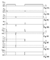
- FIGS. 9A to 9H illustrate, in chronograms, the operation of the system of FIGS. 6 to 8.
- FIG. 9A represents an example of a digital Vin signal applied at the input of the system.
- the signal is not a clock signal but a digital signal, for example for data transmission.
- FIG. 9B illustrates the shape of the signal supplied by the encoder 31 which presents a level V1 pulse at each rising edge of the signal Vin.
- the duration of the pulse depends on the time constant provided by the capacitor C72 and the on-state series resistance of the low transistor of the inverter 71.
- the voltage drops with respect to respective primary and secondary supply voltages and the digital signals are considered to have the full amplitudes of these supply voltages. Similarly, the signal propagation times have been neglected.
- FIG. 9C shows the shape of the signal supplied at the output of the encoder 32 which comprises a positive level V1 pulse at each falling edge of the signal Vin.
- the duration of the pulse depends on the value of the capacitor C76.
- the capacitors C72 and C76 are selected of the same value.
- FIG. 9D illustrates the shape of the current Ip in the primary of the transformer 11. Due to the inversion of the ground connection of this primary winding, the pulses at the output of the encoder 31 are reflected by positive pulses with orientations taken in the figures while the pulses present at the output of the encoder 32 result in negative pulses.
- FIG. 9E illustrates the shape of the voltage Vs recovered on the secondary side of the transformer.
- a positive pulse with respect to the level V ' is present at each positive pulse of the current Ip and a negative pulse with respect to the level V' is present at each negative pulse of the current Ip.
- FIG. 9F represents the appearance of the output signal of the comparator 51 which has a positive pulse of amplitude V2 while the voltage Vs is greater than the threshold TH1.
- FIG. 9G shows the appearance of the output signal of the comparator 52 which has a positive pulse of amplitude V2 while the voltage Vs is below the threshold TH2.
- FIG. 9H represents the shape of the signal Vout at the output of the flip-flop 53.
- An advantage of the present invention is that a single transformer is sufficient to achieve the galvanic isolation.
- isolation barrier is not limited to an observation window to distinguish successive fronts.
- Each pulse present on the output signal represents a front in the opposite direction with respect to the preceding edge thus simplifying the decoding system.
- doors 73 and 77 may be replaced by NAND gates if circuits 78 and 79 have odd numbers of inverters.
- the capacitors C72 and C76 are omitted and replaced by a propagation delay (for example by means of inverters in series) of the signals supplied on the first inputs of the gates 73 and 77 with respect to the signal Vin supplied on their second entries.
Landscapes
- Engineering & Computer Science (AREA)
- Power Engineering (AREA)
- Physics & Mathematics (AREA)
- Nonlinear Science (AREA)
- Multimedia (AREA)
- Computer Networks & Wireless Communication (AREA)
- Signal Processing (AREA)
- Dc Digital Transmission (AREA)
Applications Claiming Priority (1)
| Application Number | Priority Date | Filing Date | Title |
|---|---|---|---|
| FR0653735 | 2006-09-14 |
Publications (1)
| Publication Number | Publication Date |
|---|---|
| EP1901428A1 true EP1901428A1 (de) | 2008-03-19 |
Family
ID=37946465
Family Applications (1)
| Application Number | Title | Priority Date | Filing Date |
|---|---|---|---|
| EP07115966A Withdrawn EP1901428A1 (de) | 2006-09-14 | 2007-09-07 | Übertragung von digitalen Daten mit Hilfe eines Transformators |
Country Status (3)
| Country | Link |
|---|---|
| US (1) | US7961794B2 (de) |
| EP (1) | EP1901428A1 (de) |
| CN (1) | CN101146086A (de) |
Families Citing this family (9)
| Publication number | Priority date | Publication date | Assignee | Title |
|---|---|---|---|---|
| EP2282405B1 (de) | 2009-07-31 | 2016-09-14 | STMicroelectronics Srl | Signalkommunikationsvorrichtung und entsprechender Empfänger |
| EP2282406B1 (de) | 2009-07-31 | 2016-04-20 | STMicroelectronics Srl | Signalempfänger mit Störungsunterdrückung |
| US8478332B2 (en) * | 2009-07-31 | 2013-07-02 | Stmicroelectronics, S.R.L. | Receiver for signal communication system with disturbance rejection circuit |
| EP2469782B1 (de) * | 2010-12-23 | 2021-03-31 | Murrelektronik GmbH | Schaltunfsanordnung zur Übertragung von Signalen |
| CN102969904B (zh) * | 2012-11-01 | 2016-02-17 | 中国船舶重工集团公司第七二三研究所 | 一种电源及脉冲信号的高隔离传输方法 |
| CN104038204B (zh) * | 2014-05-30 | 2017-04-12 | 北京软石科技发展有限公司 | 数字信号隔离传输装置 |
| JP6688986B2 (ja) * | 2015-08-18 | 2020-04-28 | パナソニックIpマネジメント株式会社 | 信号伝送回路 |
| CN112003604B (zh) * | 2020-08-24 | 2025-06-06 | 深圳线易微电子有限公司 | 一种信号传输电路与信号传输网络 |
| CN112713893A (zh) * | 2021-01-27 | 2021-04-27 | 杭州瑞盟科技有限公司 | 一种工业控制系统及其电感耦合隔离器 |
Citations (3)
| Publication number | Priority date | Publication date | Assignee | Title |
|---|---|---|---|---|
| JPS6212239A (ja) * | 1985-07-10 | 1987-01-21 | Hitachi Ltd | デ−タ通信方式 |
| JPS63237617A (ja) * | 1987-03-26 | 1988-10-04 | Matsushita Electric Ind Co Ltd | Ami符号化回路 |
| JP2003204362A (ja) * | 2002-01-09 | 2003-07-18 | Nec Infrontia Corp | Isdn端末装置のs/t点インターフェース |
Family Cites Families (4)
| Publication number | Priority date | Publication date | Assignee | Title |
|---|---|---|---|---|
| US4300095A (en) * | 1979-08-22 | 1981-11-10 | Rockwell International Corporation | Self excited saturatable core magnetic field detection apparatus |
| US5786687A (en) * | 1996-12-03 | 1998-07-28 | Compaq Computer Corporation | Transformer-isolated pulse drive circuit |
| US7489526B2 (en) * | 2004-08-20 | 2009-02-10 | Analog Devices, Inc. | Power and information signal transfer using micro-transformers |
| US7200014B1 (en) * | 2004-11-22 | 2007-04-03 | Linear Technology Corporation | System and method for transferring duty cycle information in an isolated DC/DC converter or other circuit |
-
2007
- 2007-09-07 EP EP07115966A patent/EP1901428A1/de not_active Withdrawn
- 2007-09-12 US US11/900,605 patent/US7961794B2/en not_active Expired - Fee Related
- 2007-09-14 CN CNA2007101538882A patent/CN101146086A/zh active Pending
Patent Citations (3)
| Publication number | Priority date | Publication date | Assignee | Title |
|---|---|---|---|---|
| JPS6212239A (ja) * | 1985-07-10 | 1987-01-21 | Hitachi Ltd | デ−タ通信方式 |
| JPS63237617A (ja) * | 1987-03-26 | 1988-10-04 | Matsushita Electric Ind Co Ltd | Ami符号化回路 |
| JP2003204362A (ja) * | 2002-01-09 | 2003-07-18 | Nec Infrontia Corp | Isdn端末装置のs/t点インターフェース |
Also Published As
| Publication number | Publication date |
|---|---|
| US7961794B2 (en) | 2011-06-14 |
| US20080069249A1 (en) | 2008-03-20 |
| CN101146086A (zh) | 2008-03-19 |
Similar Documents
| Publication | Publication Date | Title |
|---|---|---|
| US6493394B2 (en) | Signal transmission system for transmitting signals between lsi chips, receiver circuit for use in the signal transmission system, and semiconductor memory device applying the signal transmission system | |
| EP0594834B1 (de) | In Standard-CMOS-Technologie realisierte, zwischen einer Logikschaltung mit niedriger Versorgungsspannung und einer Ausgangsstufe mit hoher Versorgungsspannung, liegende Schaltung | |
| US8582669B2 (en) | Noise reduction circuit in a digital isolator system | |
| US7961794B2 (en) | Transfer of digital data through a transformer | |
| KR20080095613A (ko) | 단일 신호-차동 신호 변환기 및 변환 방법 | |
| FR2967510A1 (fr) | Conversion de protocole de communication sur bus unifilaire | |
| EP0306392B1 (de) | Abfühlschaltung für Adressenumschaltungen | |
| FR2683371A1 (fr) | Memoire-tampon d'entree d'adresse d'un dispositif de memoire a semiconducteurs. | |
| TW445719B (en) | Synchronous delay circuit | |
| EP1940025A1 (de) | Übertragung von digitalen Daten über eine Trennschaltung | |
| KR100447217B1 (ko) | 새로운배선시스템용신호전송및수신장치 | |
| FR2783649A1 (fr) | Circuit de filtrage d'un signal d'horloge | |
| JPH09270683A (ja) | 相補型クロック発生器 | |
| US6661269B2 (en) | Selectively combining signals to produce desired output signal | |
| WO2004105245A3 (en) | Half-swing line precharge method and apparatus | |
| FR3023412A1 (de) | ||
| EP0277855A1 (de) | Binärer-bipolarer Umsetzer | |
| US5723994A (en) | Level boost restoration circuit | |
| KR100646291B1 (ko) | 스윙이 감소된 차동 클록에 관한 방법 및 수신기 시스템 | |
| FR3075519A1 (fr) | Dispositif de filtrage de signaux, notamment des signaux d'un bus i2c | |
| KR980003982A (ko) | 전송 평형신호의 디지털 데이터 복원 방법 및 시스템 | |
| FR2509930A1 (fr) | Circuit de pilotage par impulsions pour convertisseurs et amplificateurs de puissance | |
| FR2649265A1 (fr) | Circuit amplificateur-separateur pour la conversion ttl-cmos | |
| EP0165640B1 (de) | Vorrichtung zur galvanischen Isolierung zwischen einem Impulsgeber und einer Belastung | |
| EP3182617A1 (de) | Optischer empfänger mit relativer phasendetektion |
Legal Events
| Date | Code | Title | Description |
|---|---|---|---|
| PUAI | Public reference made under article 153(3) epc to a published international application that has entered the european phase |
Free format text: ORIGINAL CODE: 0009012 |
|
| AK | Designated contracting states |
Kind code of ref document: A1 Designated state(s): AT BE BG CH CY CZ DE DK EE ES FI FR GB GR HU IE IS IT LI LT LU LV MC MT NL PL PT RO SE SI SK TR |
|
| AX | Request for extension of the european patent |
Extension state: AL BA HR MK YU |
|
| 17P | Request for examination filed |
Effective date: 20080821 |
|
| 17Q | First examination report despatched |
Effective date: 20080925 |
|
| AKX | Designation fees paid |
Designated state(s): DE FR GB |
|
| STAA | Information on the status of an ep patent application or granted ep patent |
Free format text: STATUS: THE APPLICATION IS DEEMED TO BE WITHDRAWN |
|
| 18D | Application deemed to be withdrawn |
Effective date: 20090206 |