EP0306392B1 - Abfühlschaltung für Adressenumschaltungen - Google Patents
Abfühlschaltung für Adressenumschaltungen Download PDFInfo
- Publication number
- EP0306392B1 EP0306392B1 EP88402130A EP88402130A EP0306392B1 EP 0306392 B1 EP0306392 B1 EP 0306392B1 EP 88402130 A EP88402130 A EP 88402130A EP 88402130 A EP88402130 A EP 88402130A EP 0306392 B1 EP0306392 B1 EP 0306392B1
- Authority
- EP
- European Patent Office
- Prior art keywords
- input
- signal
- output
- circuit
- gate
- Prior art date
- Legal status (The legal status is an assumption and is not a legal conclusion. Google has not performed a legal analysis and makes no representation as to the accuracy of the status listed.)
- Expired - Lifetime
Links
- 230000007704 transition Effects 0.000 title claims description 33
- 238000001514 detection method Methods 0.000 title claims description 7
- 238000005516 engineering process Methods 0.000 description 17
- 238000010586 diagram Methods 0.000 description 5
- 230000000630 rising effect Effects 0.000 description 5
- 239000003990 capacitor Substances 0.000 description 2
- 230000003111 delayed effect Effects 0.000 description 2
- 230000006870 function Effects 0.000 description 2
- 150000002500 ions Chemical class 0.000 description 2
- 230000001934 delay Effects 0.000 description 1
- 238000010200 validation analysis Methods 0.000 description 1
Images


Classifications
-
- G—PHYSICS
- G11—INFORMATION STORAGE
- G11C—STATIC STORES
- G11C8/00—Arrangements for selecting an address in a digital store
- G11C8/18—Address timing or clocking circuits; Address control signal generation or management, e.g. for row address strobe [RAS] or column address strobe [CAS] signals
Definitions
- the present invention relates to a circuit for detecting address transitions in an integrated circuit. Increasingly, to reduce the consumption of integrated circuits, they are only activated when there is a change at the input of the level of address signals or validation signals of the circuit. When nothing happens, the circuit consumption is low, but nevertheless not zero. Address transition detection circuits are already known and make it possible to detect a level change or an input edge.
- the circuits commonly used are generally composed of chains of reversers.
- the detection method consists in measuring the level of the signals at different points in this chain and combining them in logic gates with the input signal so as to obtain an output pulse when there is a change in input level.
- US-A-4,337,525 gives an example.
- the pulse generated at output as soon as there has been a change in level at input is necessarily delayed by the propagation time in the inverters because the circuit is in series.
- the duration of the pulse and its delay with respect to the transition are linked and are a function of the transfer time in the inverters. If you want a large pulse to be able to use it well, it will be all the more delayed.
- the invention proposes to remedy these drawbacks an address transition detection circuit which minimizes the delay of the pulse generated at output as soon as there is a change in level at input.
- the invention therefore relates to a circuit for detecting address transitions in an integrated circuit consisting in generating a pulse at output as soon as there has been a change of address at input, as defined in claim 1.
- FIG. 1 represents a circuit for detecting address transitions according to the prior art in CMOS technology.
- the input terminal 1 of this circuit is connected to an adapter block 2 of TTL technology (for transistor transistor logic in English) in CMOS technology of known type.
- TTL technology for transistor transistor logic in English
- the signals processed in an integrated circuit in CMOS technology can come from external circuits produced in different technology, for example in bipolar TTL technology.
- This adapter 2 allows you to work on voltages of 0 Volt or 5 Volts.
- the output 3 of the adapter block 2 arrives at the input of an inverter I1, followed by a capacitor C1 in parallel.
- the output 4 of the inverter I1 arrives at the input of an inverter I2, followed by a capacitor C2 in parallel.
- the output 5 of the inverter I2, the output 4 of the inverter I1 and the output 3 of the adapter block 2 arrive on the input of a logic comparison block 6.
- the capacities C1 and C2 added in parallel behind each inverter I1 and I2 allow to increase the transfer time in each inverter.
- the transfer time in an inverter is of the order of one nanosecond. Adding a capacity increases this time by approximately 2 to 3 ns per inverter. It is voluntarily that we seek a longer transfer time. Because when comparing the signals in 3, 4 or 5 in the comparison logic block 6 in the absence of capacity, it can be difficult to see that the signals in 4 and 5, for example, have the same value for only 1 ns.
- the pulse is obtained at output 7 of the comparison logic block 6.
- the pulse generated in 7 is generally not of good quality and is not really usable in a reliable manner as it is. This is due to the fact that the comparison logic block 6 and the inverters I1, I2 contain a large number of transistors. It will be necessary to reshape the pulse generated at 7 in a known type circuit 8, put in series in the assembly. This circuit significantly delays the pulse generated. The output 9 of this circuit 8 will activate the following circuit, not shown here, as soon as a pulse has been generated.
- the comparison logic block 6 consists of logic gates. It receives as input the signals S3, on terminal 3, S4 on terminal 4, S5 on terminal 5 and must generate a pulse at output 7 as soon as there has been a level change at input 1.
- FIG. 2 represents among other things the time diagrams of the signals S3, S4, S5.
- the transfer time in the inverter I1 followed by the capacity C1 is t1.
- the transfer time in the inverter I2 followed by the capacity C2 is t2.
- the signal denoted S3 represents an address transition from 0V to 5V then from 5V to 0V.
- the signal S4 is inverted and the address transitions arrive with the delay t1.
- the signal S5 is inverted with respect to the signal S4.
- the transition arrives with the delay t2. It also arrives with the delay t1 + t2 with respect to the transition of the signal S3.
- the block of logic gates 6 can consist of the combination of logic gates represented in FIG. 3. This example is not the alone, there are other possible combinations.
- the output 3 of the adapter block and the output 4 of the inverter I1 constitute the inputs of an AND logic gate 31 internationally known under the name AND.
- the output 4 and the inverter I1 and the output 5 of the inverter I2 constitute the inputs of another AND gate 33.
- the output 32 of the AND gate 31 and the output 34 of the AND gate 33 constitute the inputs of an NI 35 logic gate internationally known under the name NOR.
- the output of this NI 35 gate arrives at terminal 7.
- FIG. 2 also represents the time diagram of the signals S32 on terminal 32, S34 on terminal 34 and S7 on terminal 7.
- the delay linked to the AND gate 31 is t31.
- the delay linked to the AND gate 33 is t33.
- the delay linked to the NI 35 gate is t35.
- a pulse 21 of duration t1 is obtained at 32 having a delay t31 with respect to the rising edge of the transition of the signal S3.
- a pulse 22 of duration t2 is obtained at 34 having a delay t1 + t33 relative to the falling edge of the transition of the signal S3.
- the first 21 corresponds to the rising edge of the transition of the signal S3 its delay is t31 + t35 and its duration is t1
- the second 22 corresponds to the falling edge of the transition of the signal S3 its delay is t1 + t33 + t35 and its duration is t2.
- At least one of these pulses will have a delay linked to the transfer time of one of the inverters. In the example described above, this is the second pulse 22 and this delay is t1.
- a different arrangement of the logic gates of block 6 could give a delay on the first pulse.
- the duration of these pulses is a function of the transfer time in the inverters.
- the circuit according to the invention minimizes this delay because the elements of this circuit are no longer in series but in parallel.
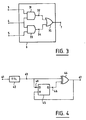
- FIG. 4 represents a circuit for detecting address transitions according to the invention.
- the input terminal 41 is connected as before to an adapter block 42 of TTL technology in CMOS technology.
- the output 43 of the adapter block 42 is connected on the one hand, to one of the inputs of a comparator 44 and on the other hand, to the input 48 of a controlled memory 45.
- the example represents an exclusive OR gate as comparator and a flip-flop D as controlled memory.
- the output 46 of flip-flop D arrives at the other input of the exclusive OR gate.
- the output of the exclusive OR gate is done on terminal 47.
- the signal S47 on terminal 47 also serves as a clock signal on terminal H of flip-flop D.
- the circuit to be activated as soon as an address transition has been detected will be connected in series with the comparator on terminal 47. It is not shown in this figure. It is possible to use other comparators or other types of memory.
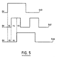
- the signal S43 on terminal 43 and the signal S46 on terminal 46 are continuously compared in the exclusive OR gate 44.
- the signal S46 is the stored signal. It has the state of the signal S43 before the transition.
- the signal S47 is of a first logic level as long as the signals S43 and S46 have the same logic level. As soon as the signals S43 and S46 take different logic levels, the signal S47 goes to a second logic level.
- the first level is the low level when the signals S43 and S46 have the same value.
- the second level is the high level when the signals S43 and S46 have different values.
- the signal S46 is memorized on the rising edge of the clock signal S47. In CMOS technology, the high level is 5 Volts and the low level is 0 Volts.
- the signal S47 goes high.
- the rising edge of a pulse is generated at 47 which corresponds to the detection of a change in level of the signal S43.
- the clock signal S47 on the terminal H of the flip-flop D activates the storage command.
- the signal S46 takes the new value of the signal S43 after the transition.
- the signals S43 and S46 having the same value again, the signal S47 goes low.
- the delay of the output pulse 47 with respect to the transition at 43 corresponds to the transfer time t3 in the exclusive OR gate 44.
- the duration of the pulse generated is equal to the sum of the transfer time t4 in the flip-flop D 45 and the transfer time t3 in the exclusive OR gate 44.
- FIG. 6 represents a particular embodiment of an address transition circuit in CMOS technology according to the invention.
- the circuit is entered on terminal 60. It is followed by an adapter block 62 of TTL technology in CMOS technology.
- the output 63 of this block 62 is connected on the one hand to one of the inputs of the comparator 64 and on the other hand to the input 61 of a controlled memory 65.
- Comparator 64 consists of an exclusive NI gate.
- the commanded memory 65 is a flip-flop D.
- An exclusive NI gate cannot be produced in a simple manner in CMOS technology.
- the circuitry 642 is called "pseudo-inverter" because it is either an inverter or a non-inverting amplifier following the value of the signals present on the outputs Q 66 and Q 67 of scale D 65.
- the transistors T1 of PMOS type and T2 of NMOS type form the transfer gate 641.
- the source S′1 of the transistor T1 is connected to the drain D2 of the transistor T2. They are supplied by the signal S63 on terminal 63.
- the drain D1 of the transistor T1 is connected to the source S′2 of the transistor T2 on the output terminal 68 of the exclusive OR gate (641, 642).
- the gate G1 of the transistor T1 receives the signal S66 which corresponds to the output Q 66 of the flip-flop D 65.
- the gate G2 of the transistor T2 receives the signal S67 which corresponds to the output Q 67 of scale D 65.
- the transistors T3 of the PMOS type and T4 of the NMOS type form the "pseudo-inverter" 642.
- the drain D3 of the transistor T3 is connected to the drain D4 of the transistor T4 on the output terminal 68 of the exclusive OR gate (641, 642).
- the source S′3 of the transistor T3 receives the signal S66 which corresponds to the output 66 of the flip-flop D 65.
- the source S′4 of the transistor T4 receives the signal S67 which corresponds to the output 67 of the flip-flop D 65.
- the gate G3 of the transistor T3 and the gate G4 of the transistor T4 are common and are supplied by the signal S63.
- the signal S68 on terminal 68 at the output of the exclusive OR gate (641, 642) is inverted with respect to the input signal S63 on terminal 63.
- the signal S68 on terminal 68 at the output of the exclusive OR gate (641, 642) is of the same level as the input signal S63 on terminal 63.
- the signal S68 is then inverted in an inverter 643 formed of transistors T5 of the PMOS type and T6 of the NMOS type.
- the signal S68 arrives on the gate G6 of the transistor T6, the gate G5 of the transistor T5 is grounded.
- the source S′5 of the transistor T5 is brought to the potential + V supply voltage of the circuit.
- the source S′6 of the transistor T6 is grounded.
- the drains D5 of the transistor T5 and D6 of the transistor T6 are common on the terminal 69.
- the signal S69 on the terminal 69 feeds the circuit which one wants to activate but it is not represented here.
- This signal S69 also serves as a clock signal on the terminal H of the D 65 flip-flop.
- the D 65 flip-flop then reacts to the falling edge of the signal S69.
- the delay and the duration of the pulse that is generated in a circuit according to the invention shown in FIG. 4 can be calculated as follows:
- the transfer time t3 in an exclusive OR gate is low on the order of 1 ns.
- the transfer time t4 in a flip-flop D is of the order of 2 to 3 ns.
- the value T will be around 4ns.
- the overall gain with a circuit according to the invention in terms of the pulse delay is of the order of 10 ns compared to the prior art.
- This circuit has only one stable state when the value of the input signal S43 is equal to the value of the stored signal S46.
- the safety of this circuit is much greater than that of the circuits used so far.
- the flip-flop 45 can also be used for something else and the value of the stored signal S46 or its inverse will be used. This will save space in the integrated circuit, which is always sought after.
Landscapes
- Engineering & Computer Science (AREA)
- Microelectronics & Electronic Packaging (AREA)
- Manipulation Of Pulses (AREA)
- Dram (AREA)
- Static Random-Access Memory (AREA)
- Logic Circuits (AREA)
Claims (3)
Applications Claiming Priority (2)
| Application Number | Priority Date | Filing Date | Title |
|---|---|---|---|
| FR8712155A FR2619939B1 (fr) | 1987-09-01 | 1987-09-01 | Circuit de detection de transitions d'adresses |
| FR8712155 | 1987-09-01 |
Publications (2)
| Publication Number | Publication Date |
|---|---|
| EP0306392A1 EP0306392A1 (de) | 1989-03-08 |
| EP0306392B1 true EP0306392B1 (de) | 1992-07-22 |
Family
ID=9354547
Family Applications (1)
| Application Number | Title | Priority Date | Filing Date |
|---|---|---|---|
| EP88402130A Expired - Lifetime EP0306392B1 (de) | 1987-09-01 | 1988-08-19 | Abfühlschaltung für Adressenumschaltungen |
Country Status (5)
| Country | Link |
|---|---|
| US (1) | US4922122A (de) |
| EP (1) | EP0306392B1 (de) |
| JP (1) | JP2824444B2 (de) |
| DE (1) | DE3872988T2 (de) |
| FR (1) | FR2619939B1 (de) |
Families Citing this family (18)
| Publication number | Priority date | Publication date | Assignee | Title |
|---|---|---|---|---|
| US5228003A (en) * | 1988-04-15 | 1993-07-13 | Seiko Epson Corporation | Semiconductor memory |
| JPH01280923A (ja) * | 1988-05-07 | 1989-11-13 | Mitsubishi Electric Corp | 半導体集積回路装置 |
| JPH02131010A (ja) * | 1988-11-10 | 1990-05-18 | Fujitsu Ltd | アドレス変化検出回路 |
| US5199002A (en) * | 1990-10-01 | 1993-03-30 | Integrated Device Technology, Inc. | SRAM-address-change-detection circuit |
| US5124584A (en) * | 1990-10-22 | 1992-06-23 | Sgs-Thomson Microelectronics, Inc. | Address buffer circuit with transition-based latching |
| US5304874A (en) * | 1991-05-31 | 1994-04-19 | Thunderbird Technologies, Inc. | Differential latching inverter and random access memory using same |
| EP0525270A1 (de) * | 1991-07-31 | 1993-02-03 | International Business Machines Corporation | BICMOS-lokale Adressenübergangsabfühlschaltung |
| JPH07141889A (ja) * | 1993-06-22 | 1995-06-02 | Sharp Corp | 半導体記憶装置 |
| US5418479A (en) * | 1993-12-27 | 1995-05-23 | Intel Corporation | Method and circuitry for generating a safe address transition pulse in a memory device |
| JPH07230691A (ja) * | 1994-02-16 | 1995-08-29 | Fujitsu Ltd | 半導体記憶装置 |
| US5471157A (en) * | 1994-03-31 | 1995-11-28 | Sgs-Thomson Microelectronics, Inc. | Integrated circuit with centralized control of edge transition detection pulse generation |
| FR2724483B1 (fr) * | 1994-09-12 | 1996-12-27 | Sgs Thomson Microelectronics | Procede de decodage d'adresse dans une memoire en circuit integre et circuit memoire mettant en oeuvre le procede |
| US5493538A (en) * | 1994-11-14 | 1996-02-20 | Texas Instruments Incorporated | Minimum pulse width address transition detection circuit |
| JPH0982085A (ja) * | 1995-09-13 | 1997-03-28 | Sharp Corp | 半導体記憶装置 |
| US5907250A (en) * | 1997-05-16 | 1999-05-25 | International Business Machines Corporation | Transition detector with timer |
| US6304104B1 (en) * | 1999-09-13 | 2001-10-16 | Rambus, Inc. | Method and apparatus for reducing worst case power |
| EP2376964A1 (de) * | 2008-12-19 | 2011-10-19 | Abbott Laboratories | Verfahren und vorrichtung zum detektieren von objekttr?ger-deckgl?sern |
| CN103310832B (zh) * | 2012-03-12 | 2015-11-25 | 旺宏电子股份有限公司 | 侦测地址转变的电路与方法 |
Family Cites Families (10)
| Publication number | Priority date | Publication date | Assignee | Title |
|---|---|---|---|---|
| JPS55138128A (en) * | 1979-04-17 | 1980-10-28 | Nec Corp | Memory circuit |
| US4337525A (en) * | 1979-04-17 | 1982-06-29 | Nippon Electric Co., Ltd. | Asynchronous circuit responsive to changes in logic level |
| JPS5792484A (en) * | 1980-11-28 | 1982-06-09 | Toshiba Corp | Timing pulse generating circuit |
| DE3274709D1 (en) * | 1982-03-04 | 1987-01-22 | Itt Ind Gmbh Deutsche | Insulated-gate field-effect transistor circuit for a one out of n system |
| US4446389A (en) * | 1982-03-15 | 1984-05-01 | Ampex Corporation | Quadrature tach decoder circuit |
| US4539661A (en) * | 1982-06-30 | 1985-09-03 | Fujitsu Limited | Static-type semiconductor memory device |
| US4496861A (en) * | 1982-12-06 | 1985-01-29 | Intel Corporation | Integrated circuit synchronous delay line |
| JPS60242580A (ja) * | 1984-05-16 | 1985-12-02 | Hitachi Micro Comput Eng Ltd | Mosスタテイツク型ram |
| US4598216A (en) * | 1984-08-27 | 1986-07-01 | Ncr Corporation | Assist circuit for a data bus in a data processing system |
| JPS61258391A (ja) * | 1985-05-13 | 1986-11-15 | Seiko Epson Corp | アドレス遷移検出回路 |
-
1987
- 1987-09-01 FR FR8712155A patent/FR2619939B1/fr not_active Expired
-
1988
- 1988-08-19 EP EP88402130A patent/EP0306392B1/de not_active Expired - Lifetime
- 1988-08-19 DE DE8888402130T patent/DE3872988T2/de not_active Expired - Fee Related
- 1988-08-23 US US07/235,324 patent/US4922122A/en not_active Expired - Lifetime
- 1988-09-01 JP JP63219598A patent/JP2824444B2/ja not_active Expired - Lifetime
Also Published As
| Publication number | Publication date |
|---|---|
| DE3872988D1 (de) | 1992-08-27 |
| JP2824444B2 (ja) | 1998-11-11 |
| JPS6470991A (en) | 1989-03-16 |
| DE3872988T2 (de) | 1993-03-04 |
| FR2619939B1 (fr) | 1989-12-08 |
| FR2619939A1 (fr) | 1989-03-03 |
| US4922122A (en) | 1990-05-01 |
| EP0306392A1 (de) | 1989-03-08 |
Similar Documents
| Publication | Publication Date | Title |
|---|---|---|
| EP0306392B1 (de) | Abfühlschaltung für Adressenumschaltungen | |
| FR2666436A1 (fr) | Memoire a semi-conducteurs a acces rapide. | |
| NL8100741A (nl) | Signaalopneemschakeling. | |
| FR2687488A1 (fr) | Dispositif pour memoire a semi-conducteurs avec un circuit de generation d'un signal d'horloge pour des lignes de bit separees. | |
| FR2584849A1 (fr) | Circuit tampon de sortie a semi-conducteurs a grille isolee par oxyde metallique, pour memoire rapide | |
| EP0262013A1 (de) | Leseverstärker | |
| FR2664080A1 (fr) | Circuit de pilotage d'ecriture ayant des moyens de precharge. | |
| EP0977407A1 (de) | Verstärker mit zeitvarianter Ausgangsleistung | |
| FR2679672A1 (fr) | Circuit de transmission de donnees avec des lignes d'entree/sortie segmentees. | |
| FR2533739A1 (fr) | Memoire a semiconducteurs | |
| FR2499788A1 (fr) | Circuit generateur d'impulsions utilisant une source de courant et ensemble de memorisation utilisant un tel circuit | |
| FR2647581A1 (fr) | Circuit pour l'ajustement d'un niveau de tension de sortie de donnees dans un dispositif de memoire a semiconducteurs | |
| EP0271406B1 (de) | Anordnung zur Selbstsynchronisierung von Ausgangsschaltungen eines Speichers | |
| FR2787212A1 (fr) | Circuit pour remettre a l'etat initial une paire de bus de donnees d'un dispositif de memoire a semiconducteur | |
| FR2630870A1 (fr) | Portes logiques | |
| EP0685848B1 (de) | Umwandlungsdetektorgerät zur Erzeugung eines Pulses mit variabler Zeitdauer | |
| EP0897182B1 (de) | Strahlungsunempfindliche statische Speicherzelle | |
| KR100289341B1 (ko) | 반도체 메모리 장치의 어드레스 천이 검출 회로 | |
| US5796674A (en) | Signal transition detection circuit | |
| FR2810438A1 (fr) | Circuit de detection d'usure | |
| JPH0955087A (ja) | 半導体メモリ装置 | |
| FR2810150A1 (fr) | Dispositif de memoire vive dynamique et procede de commande d'un acces en lecture d'une telle memoire | |
| EP3923150B1 (de) | Verfahren zur verwaltung von zugriffsanfragen auf einen direktzugriffsspeicher und entsprechendes system | |
| EP0648018B1 (de) | Schaltung zur Anzeige der Phasenverhältnisse zwischen mehreren Signalen mit gleicher Frequenz und ihre Anwendung in einer Schaltung zur Korrektur der Phasen zwischen diesen Signalen | |
| KR100301820B1 (ko) | 센스 앰프 |
Legal Events
| Date | Code | Title | Description |
|---|---|---|---|
| PUAI | Public reference made under article 153(3) epc to a published international application that has entered the european phase |
Free format text: ORIGINAL CODE: 0009012 |
|
| AK | Designated contracting states |
Kind code of ref document: A1 Designated state(s): DE ES GB IT NL |
|
| 17P | Request for examination filed |
Effective date: 19890323 |
|
| 17Q | First examination report despatched |
Effective date: 19910626 |
|
| GRAA | (expected) grant |
Free format text: ORIGINAL CODE: 0009210 |
|
| AK | Designated contracting states |
Kind code of ref document: B1 Designated state(s): DE ES GB IT NL |
|
| PG25 | Lapsed in a contracting state [announced via postgrant information from national office to epo] |
Ref country code: NL Effective date: 19920722 Ref country code: ES Free format text: THE PATENT HAS BEEN ANNULLED BY A DECISION OF A NATIONAL AUTHORITY Effective date: 19920722 |
|
| REF | Corresponds to: |
Ref document number: 3872988 Country of ref document: DE Date of ref document: 19920827 |
|
| ITF | It: translation for a ep patent filed | ||
| GBT | Gb: translation of ep patent filed (gb section 77(6)(a)/1977) | ||
| NLV1 | Nl: lapsed or annulled due to failure to fulfill the requirements of art. 29p and 29m of the patents act | ||
| PLBE | No opposition filed within time limit |
Free format text: ORIGINAL CODE: 0009261 |
|
| STAA | Information on the status of an ep patent application or granted ep patent |
Free format text: STATUS: NO OPPOSITION FILED WITHIN TIME LIMIT |
|
| 26N | No opposition filed | ||
| PGFP | Annual fee paid to national office [announced via postgrant information from national office to epo] |
Ref country code: DE Payment date: 20000814 Year of fee payment: 13 |
|
| REG | Reference to a national code |
Ref country code: GB Ref legal event code: IF02 |
|
| PG25 | Lapsed in a contracting state [announced via postgrant information from national office to epo] |
Ref country code: DE Free format text: LAPSE BECAUSE OF NON-PAYMENT OF DUE FEES Effective date: 20020501 |
|
| PGFP | Annual fee paid to national office [announced via postgrant information from national office to epo] |
Ref country code: GB Payment date: 20020814 Year of fee payment: 15 |
|
| PG25 | Lapsed in a contracting state [announced via postgrant information from national office to epo] |
Ref country code: GB Free format text: LAPSE BECAUSE OF NON-PAYMENT OF DUE FEES Effective date: 20030819 |
|
| GBPC | Gb: european patent ceased through non-payment of renewal fee |
Effective date: 20030819 |
|
| PG25 | Lapsed in a contracting state [announced via postgrant information from national office to epo] |
Ref country code: IT Free format text: LAPSE BECAUSE OF NON-PAYMENT OF DUE FEES Effective date: 20050819 |