EP1906533A1 - Circuit d'entrée numérique avec un composant opto-électronique - Google Patents
Circuit d'entrée numérique avec un composant opto-électronique Download PDFInfo
- Publication number
- EP1906533A1 EP1906533A1 EP06020510A EP06020510A EP1906533A1 EP 1906533 A1 EP1906533 A1 EP 1906533A1 EP 06020510 A EP06020510 A EP 06020510A EP 06020510 A EP06020510 A EP 06020510A EP 1906533 A1 EP1906533 A1 EP 1906533A1
- Authority
- EP
- European Patent Office
- Prior art keywords
- digital input
- transistor
- input
- constant current
- resistor
- Prior art date
- Legal status (The legal status is an assumption and is not a legal conclusion. Google has not performed a legal analysis and makes no representation as to the accuracy of the status listed.)
- Ceased
Links
- 230000005693 optoelectronics Effects 0.000 title claims description 16
- 230000008054 signal transmission Effects 0.000 claims abstract description 5
- 239000003990 capacitor Substances 0.000 claims description 6
- 238000009499 grossing Methods 0.000 claims description 2
- 230000003321 amplification Effects 0.000 description 2
- 238000003199 nucleic acid amplification method Methods 0.000 description 2
- 241000859095 Bero Species 0.000 description 1
- 230000005540 biological transmission Effects 0.000 description 1
- 230000001419 dependent effect Effects 0.000 description 1
- 238000011161 development Methods 0.000 description 1
- 230000018109 developmental process Effects 0.000 description 1
- 238000000926 separation method Methods 0.000 description 1
Images
Classifications
-
- H—ELECTRICITY
- H03—ELECTRONIC CIRCUITRY
- H03K—PULSE TECHNIQUE
- H03K17/00—Electronic switching or gating, i.e. not by contact-making and –breaking
- H03K17/51—Electronic switching or gating, i.e. not by contact-making and –breaking characterised by the components used
- H03K17/78—Electronic switching or gating, i.e. not by contact-making and –breaking characterised by the components used using opto-electronic devices, i.e. light-emitting and photoelectric devices electrically- or optically-coupled
-
- H—ELECTRICITY
- H03—ELECTRONIC CIRCUITRY
- H03K—PULSE TECHNIQUE
- H03K17/00—Electronic switching or gating, i.e. not by contact-making and –breaking
- H03K17/94—Electronic switching or gating, i.e. not by contact-making and –breaking characterised by the way in which the control signals are generated
Definitions
- the invention relates to a digital input for transmitting digital signals from a signal generator, in particular a proximity switch, with an opto-electronic connection component.
- Proximity switches are proximity sensors, ie non-contact. If you want to use a proximity switch, you must pay attention to the quiescent current of the proximity switch.
- the operating voltage is the one common to the series of proximity switches and digital input. Therefore, a quiescent current in an idle state always flows through the digital input, the proximity switch for its own operation requires the quiescent current.
- a conventional, passively connected digital input has a linear characteristic which, on the one hand, has an increasing power loss with increasing input voltage of the digital input and, on the other hand, can not deliver the quiescent current required for a proximity switch.
- a conventional digital input has a high level (logic high) between 15V and 30V and a low level (logic low) between -3V and 5V.
- logic high logic high
- low logic low
- a relatively high current flows in the digital input, which consequently leads to a relatively high power loss.
- a 2-wire proximity switch (2-wire connection) is used on a digital input, then the proximity switch should be allowed a quiescent current through the digital input without the digital input being switched on.
- the invention has for its object to provide a digital input for transmitting digital signals from a signal generator, in particular a proximity switch and to reduce the power loss of the digital input.
- the invention is based on the idea of enabling a quiescent current through a digital input in order to ensure safe operation of a proximity switch connected to this digital input.
- a digital input is suitable for transmission of digital signals from a signal generator, such as a PLC (programmable logic controller), the digital input having an opto-electronic connection component, eg an optocoupler, for galvanically isolated signal transmission.
- the output of the digital input is then formed by means of the opto-electronic connection component.
- the digital input must have at least two constant current sources. In this case, a first constant current source is provided for limiting the value of a flow current of the digital input to a current value.
- the input current of the opto-electronic connecting element is thereby limited.
- the current value is predetermined depending on the wiring of the first constant current source or on the switching threshold of the opto-electronic connecting element. Limiting the flow current can reduce the current consumption in the digital input so that the power loss of the digital input can be kept low.
- a second constant current source is provided for providing and / or limiting a quiescent current through the digital input. The quiescent current is necessary for the operation of the proximity switch.
- the optoelectronic connection component or the digital input is not switched on, ie a logic low (eg 0V) is shown at the output of the digital input or the optoelectronic connection element because the switching threshold of the optoelectronic connection element electronic connection element is not exceeded.
- a logic low eg 0V
- the first and second constant current sources are two conventional transistor constant current sources, and each has first and second current amplification transistors.
- the first constant current source has a first resistor, a second resistor and a first Zener diode, wherein the first resistor is provided for limiting the base current of the first transistor and for limiting the current through the first zener diode, wherein the second resistor to Determining the collector current of the first transistor between the emitter of the first transistor and a reference voltage terminal (usually grounded with potential "zero") is connected and wherein the first Zener diode for fixing the base voltage of the first transistor between the base of the first transistor and the Reference voltage connection is connected,
- the second constant current source in addition to the second transistor to a third resistor, a fourth resistor and a second Zener diode.
- the third resistor for limiting the base current of the second transistor and for limiting the current through the second Zener diode between the collector and the base of the second transistor is connected.
- the fourth resistor is used to determine the collector current of the second transistor between the emitter of the second transistor and the reference voltage terminal and the second Zener diode is connected between the base of the second transistor and the reference voltage terminal to establish the base voltage of the second transistor.
- an electrical path is provided between an input of the digital input and a first input of the opto-electronic connection component.
- the second constant current source is connected in parallel with the first constant current source between the input of the digital input and the first constant current source on the electrical path.
- the collector of the second transistor between the input of the digital input and the first constant current source can be connected to the electrical path.
- the collector of the first transistor is connected to the second input of the opto-electronic connection component, and the first resistor connected between the electrical path and the base of the first transistor.
- the digital input may be directly or indirectly connected to another device, e.g., via the opto-electronic interconnect device, e.g. Controller, connected.
- a capacitor for smoothing the input voltage of the digital input and for EMC strength between the input of the digital input and the two constant current sources is connected to the electrical path such that the capacitor is arranged in parallel with the two constant current sources.
- the current through the first and second constant current sources can flow sequentially and be more stably limited to a current value.
- a diode for protecting the digital input is connected in front of a negative voltage in the electrical path.
- one with the digital input verbundner proximity switches are protected against a backward current.
- a light-emitting diode is provided for displaying a state of the digital input. This makes it clear and identifiable in which state the digital input is up-to-date.
- a third Zener diode for setting a switching threshold of the digital input is switched to the electrical path.
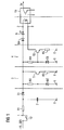
- the proximity switch 12 requires for its own operation, the quiescent current, the quiescent current in the idle state always flows through the digital input, even if the digital input was not turned on.
- the digital input has two constant current sources 4 and 5 and an optocoupler 10 for signal transmission with potential separation, wherein the optocoupler 10 has a first input 2 and a second input 3.
- the digital input is connected via the optocoupler 10 to a controller. An electrical path is between an input 1 of the digital input and the first input 2 of the optocoupler 10 is formed.
- the first constant current source 4 and the second constant current source 5 are two conventional transistor constant current sources. They each occupy a first transistor T2 and a second transistor T1 for current amplification.
- the first constant current source 4 has a first resistor R4, a second resistor R5, and a first Zener diode D3
- the second constant current source 5 has a third resistor R2, a fourth resistor R3, and a second Zener diode D2.
- the two constant current sources are connected in parallel to the electrical path.
- the current through the first and second constant current sources can flow sequentially and be more stably limited to a current value.
- the input current of the optocoupler 10 is limited to a predetermined current value, wherein the value, for example.
- the second constant current source 5 a quiescent current, which is necessary for the operation of the proximity switch 12, is provided and also limited, even if the digital input is not turned on, i. shows a logic low at the output of the digital input.
- the output current of the digital input can achieve a predetermined current value faster or with a lower output voltage.
- a corresponding base voltage of the first transistor T2 is generated by means of the Zener diode D3 by the first Zener diode D3 between the base and the ground (ground) 6 is connected.
- the first resistor R4 is connected to limit the base current of the first transistor T2 and to limit the current flowing through the first zener diode D3 between the electrical path and the base of the first transistor T2.
- the second resistor R5 is connected to determine the collector current of the first transistor T2 between the emitter and the ground 6, and the collector of the first transistor T2 is connected to the second input 3 of the optocoupler 10 to operate the optocoupler 10.
- the second zener diode D2 for fixing the base voltage of the second transistor T1 is connected between the base of the second transistor T2 and the ground 6.
- the third resistor R2 is connected to limit the base current of the second transistor T1 and to limit the current flowing through the second Zener diode D2 between the collector and the base of the second transistor T1.
- the fourth resistor R3 is connected between the emitter of the second transistor T1 and the ground 6 to determine the collector current.
- the collector of the second transistor T1 is connected between the input 1 and the first constant current source 4 at the electrical path.
- a fifth resistor R1 for protection of the digital input is switched on the side of input 1 of the digital input in the electrical path.
- a capacitor 7 between the input 1 and the two constant current sources 4 and 5 is connected to the electrical path such that the capacitor 7 is arranged parallel to the two constant current sources 4 and 5.
- a diode D1 is connected to protect the digital input from a negative voltage in the electrical path.
- the proximity switch 12 connected to the input 1 can also be protected by this diode D1.
- a third zener diode D4 is switched to the electrical path to set the switching threshold of the digital input.
- the status of the digital input should be displayed outside the module of the digital input.
- a light emitting diode (LED) 9 is switched to indicate a state of the digital input next to the third Zener diode D4 in the electrical path. Then it can be seen in which state the digital input is up to date.
- LED light emitting diode
- the quiescent current necessary for the operation of the proximity switch can be ensured, so that the digital input for connection with a proximity switch is compatible. Since the power consumption is limited to a certain value, the digital input is also a low-loss, low-cost and with low component cost feasible solution.
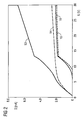
- the U / I characteristics are shown for several components of the digital input.
- the characteristic curve 14 the collector current with respect the collector-emitter voltage of the second transistor T1.
- the characteristic curve 15 the collector current of the first transistor T2, namely the input current of the optocoupler 10, with respect to the collector-emitter voltage of the first transistor T2, namely the output voltage of the digital input is shown.
- the output current of the digital input or the optocoupler 10 can be limited by the use of the first constant current source 4 to a current value of 2mA.
- a quiescent current which is necessary for the operation of the proximity switch 12, can be provided and / or limited. It can be seen from the characteristics 14 that e.g. at an input voltage of 5V the quiescent current has a value of about 1.8mA, wherein the quiescent current is not represented alone but with the vitrostrom of the second transistor T1 together by the characteristic curve 14.
Landscapes
- Electronic Switches (AREA)
Priority Applications (1)
| Application Number | Priority Date | Filing Date | Title |
|---|---|---|---|
| EP06020510A EP1906533A1 (fr) | 2006-09-29 | 2006-09-29 | Circuit d'entrée numérique avec un composant opto-électronique |
Applications Claiming Priority (1)
| Application Number | Priority Date | Filing Date | Title |
|---|---|---|---|
| EP06020510A EP1906533A1 (fr) | 2006-09-29 | 2006-09-29 | Circuit d'entrée numérique avec un composant opto-électronique |
Publications (1)
| Publication Number | Publication Date |
|---|---|
| EP1906533A1 true EP1906533A1 (fr) | 2008-04-02 |
Family
ID=37788863
Family Applications (1)
| Application Number | Title | Priority Date | Filing Date |
|---|---|---|---|
| EP06020510A Ceased EP1906533A1 (fr) | 2006-09-29 | 2006-09-29 | Circuit d'entrée numérique avec un composant opto-électronique |
Country Status (1)
| Country | Link |
|---|---|
| EP (1) | EP1906533A1 (fr) |
Cited By (7)
| Publication number | Priority date | Publication date | Assignee | Title |
|---|---|---|---|---|
| WO2009125311A1 (fr) * | 2008-04-07 | 2009-10-15 | Marzoli S.P.A. | Dispositif de commande de soufflage pour les peignes rectilignes d'une peigneuse |
| WO2012000708A1 (fr) * | 2010-06-29 | 2012-01-05 | Siemens Aktiengesellschaft | Circuit pour une entrée numérique |
| US8816747B2 (en) * | 2012-03-05 | 2014-08-26 | Siemens Aktiengesellschaft | Digital input unit |
| JP2017005290A (ja) * | 2015-06-04 | 2017-01-05 | 横河電機株式会社 | 接点入力回路 |
| DE102017131200A1 (de) | 2017-12-22 | 2019-06-27 | Pilz Gmbh & Co. Kg | Digitale Eingangsschaltung zum Empfangen digitaler Eingangssignale eines Signalgebers |
| CN111585566A (zh) * | 2020-06-10 | 2020-08-25 | 光惠(上海)激光科技有限公司 | 一种兼容5v和24v电压的隔离数字输入电路 |
| CN111884642A (zh) * | 2020-08-04 | 2020-11-03 | 西安博瑞集信电子科技有限公司 | 一种单片吸收式单刀单掷开关芯片 |
Citations (3)
| Publication number | Priority date | Publication date | Assignee | Title |
|---|---|---|---|---|
| JPS59146305A (ja) * | 1983-02-10 | 1984-08-22 | Hitachi Ltd | 電圧入力形プログラマブルコントロ−ラ |
| JPH08263110A (ja) * | 1995-03-23 | 1996-10-11 | Nippondenso Co Ltd | 制御装置の入力回路 |
| US7019318B2 (en) * | 2003-12-29 | 2006-03-28 | Schneider Automation, Sas | Dual current-source digital-input circuit for an industrial automation system |
-
2006
- 2006-09-29 EP EP06020510A patent/EP1906533A1/fr not_active Ceased
Patent Citations (3)
| Publication number | Priority date | Publication date | Assignee | Title |
|---|---|---|---|---|
| JPS59146305A (ja) * | 1983-02-10 | 1984-08-22 | Hitachi Ltd | 電圧入力形プログラマブルコントロ−ラ |
| JPH08263110A (ja) * | 1995-03-23 | 1996-10-11 | Nippondenso Co Ltd | 制御装置の入力回路 |
| US7019318B2 (en) * | 2003-12-29 | 2006-03-28 | Schneider Automation, Sas | Dual current-source digital-input circuit for an industrial automation system |
Cited By (9)
| Publication number | Priority date | Publication date | Assignee | Title |
|---|---|---|---|---|
| WO2009125311A1 (fr) * | 2008-04-07 | 2009-10-15 | Marzoli S.P.A. | Dispositif de commande de soufflage pour les peignes rectilignes d'une peigneuse |
| WO2012000708A1 (fr) * | 2010-06-29 | 2012-01-05 | Siemens Aktiengesellschaft | Circuit pour une entrée numérique |
| US8816747B2 (en) * | 2012-03-05 | 2014-08-26 | Siemens Aktiengesellschaft | Digital input unit |
| JP2017005290A (ja) * | 2015-06-04 | 2017-01-05 | 横河電機株式会社 | 接点入力回路 |
| DE102017131200A1 (de) | 2017-12-22 | 2019-06-27 | Pilz Gmbh & Co. Kg | Digitale Eingangsschaltung zum Empfangen digitaler Eingangssignale eines Signalgebers |
| CN109962700A (zh) * | 2017-12-22 | 2019-07-02 | 皮尔茨有限及两合公司 | 用于接收信号发生器的数字输入信号的数字输入电路 |
| DE102017131200B4 (de) | 2017-12-22 | 2019-09-05 | Pilz Gmbh & Co. Kg | Digitale Eingangsschaltung zum Empfangen digitaler Eingangssignale eines Signalgebers |
| CN111585566A (zh) * | 2020-06-10 | 2020-08-25 | 光惠(上海)激光科技有限公司 | 一种兼容5v和24v电压的隔离数字输入电路 |
| CN111884642A (zh) * | 2020-08-04 | 2020-11-03 | 西安博瑞集信电子科技有限公司 | 一种单片吸收式单刀单掷开关芯片 |
Similar Documents
| Publication | Publication Date | Title |
|---|---|---|
| EP2980660B1 (fr) | Procédé et dispositif de surveillance et de commutation d'un circuit de charge | |
| DE102008045968A1 (de) | Stromversorgungs-Steuergerät | |
| DE102004015528A1 (de) | Unterbrechungserfassungsschaltung für eine Sensorvorrichtung | |
| DE102007035710A1 (de) | Messumformer und Stellungsregler zum Anschließen an eine Zweileiter-Stromschleife sowie deren Verwendung | |
| EP1906533A1 (fr) | Circuit d'entrée numérique avec un composant opto-électronique | |
| DE102011015498A1 (de) | Eingangsschaltung für eine Eingangsbaugruppe und Verfahren zum Betreiben einer Eingangsschaltung | |
| EP2829929A1 (fr) | Appareil de terrain avec un affichage et/ou une unité d'entrée détachable | |
| EP3934942B1 (fr) | Appareil de commande de véhicule automobile, comportant une fonction de mise en circuit et d'arrêt pour au moins un consommateur électrique devant être commandé par l'appareil de commande de véhicule automobile | |
| WO2009015925A1 (fr) | Circuit de contrôle électronique permettant de contrôler la liaison électrique entre au moins deux appareils | |
| DE4326423B4 (de) | Anordnung zur Entkopplung eines Verbrauchers von einer Gleichspannungs-Versorgungsquelle | |
| DE19947501C5 (de) | Aktuator-Sensor-Interface-Slave | |
| DE102020111125A1 (de) | Feldgerät der Automatisierungstechnik | |
| DE102016113268A1 (de) | Verfahren und Sicherheitsschaltung zur sicheren Begrenzung der elektrischen Leistungsaufnahme | |
| DE3723008C1 (en) | Electronic switching device preferably operating contactlessly | |
| EP3333656B1 (fr) | Circuiterie pour une entrée numérique d'un module périphérique et module périphérique | |
| DE102007036680B4 (de) | Schaltungsvorrichtung zur Erkennung einer unterbrochenen Masseleitung | |
| EP0298329B1 (fr) | Appareil de commutation électronique fonctionnant de préférence sans contact | |
| DE19906342C2 (de) | Elektronisches, vorzugsweise berührungslos arbeitendes Schaltgerät | |
| DE102019002640B4 (de) | Baugruppe mit mindestens einer Schnittstellenschaltung mit einer Stromsenke oder -quelle mit optimierter Verteilung der Verlustleistung | |
| EP2780730B1 (fr) | Circuit intégré permettant de commuter des charges, circuiterie comportant un circuit intégré et une charge connectée, et procédé permettant de faire fonctionner une telle circuiterie | |
| DE10205832A1 (de) | Ansteuerung für Stromrichterventile | |
| EP1434349B1 (fr) | Circuit de protection d'un transistor contre la surtension et la surintensité de courant | |
| DE102012007776A1 (de) | Eindraht-Programmier- und Messkette | |
| DE102011076647B4 (de) | Sicherheitsgerichteter Slave | |
| WO2014167064A1 (fr) | Circuit de protection d'un étage de sortie de signal |
Legal Events
| Date | Code | Title | Description |
|---|---|---|---|
| PUAI | Public reference made under article 153(3) epc to a published international application that has entered the european phase |
Free format text: ORIGINAL CODE: 0009012 |
|
| AK | Designated contracting states |
Kind code of ref document: A1 Designated state(s): AT BE BG CH CY CZ DE DK EE ES FI FR GB GR HU IE IS IT LI LT LU LV MC NL PL PT RO SE SI SK TR |
|
| AX | Request for extension of the european patent |
Extension state: AL BA HR MK YU |
|
| 17P | Request for examination filed |
Effective date: 20080424 |
|
| 17Q | First examination report despatched |
Effective date: 20080523 |
|
| AKX | Designation fees paid |
Designated state(s): DE FR GB IT |
|
| STAA | Information on the status of an ep patent application or granted ep patent |
Free format text: STATUS: THE APPLICATION HAS BEEN REFUSED |
|
| 18R | Application refused |
Effective date: 20090214 |