EP1906574A1 - Verfahren zur Steuerung eines gemeinsamen Schutzmoduls und Vorrichtung zur Verarbeitung von optischen Wellenlängen - Google Patents
Verfahren zur Steuerung eines gemeinsamen Schutzmoduls und Vorrichtung zur Verarbeitung von optischen Wellenlängen Download PDFInfo
- Publication number
- EP1906574A1 EP1906574A1 EP07116724A EP07116724A EP1906574A1 EP 1906574 A1 EP1906574 A1 EP 1906574A1 EP 07116724 A EP07116724 A EP 07116724A EP 07116724 A EP07116724 A EP 07116724A EP 1906574 A1 EP1906574 A1 EP 1906574A1
- Authority
- EP
- European Patent Office
- Prior art keywords
- state
- wavelength channel
- wavelength
- module
- configuration
- Prior art date
- Legal status (The legal status is an assumption and is not a legal conclusion. Google has not performed a legal analysis and makes no representation as to the accuracy of the status listed.)
- Granted
Links
- 230000003287 optical effect Effects 0.000 title claims abstract description 97
- 238000012545 processing Methods 0.000 title claims abstract description 84
- 238000000034 method Methods 0.000 title claims abstract description 33
- 230000000903 blocking effect Effects 0.000 claims abstract description 32
- 230000008569 process Effects 0.000 claims description 15
- 238000003780 insertion Methods 0.000 claims description 10
- 230000037431 insertion Effects 0.000 claims description 10
- 238000000605 extraction Methods 0.000 claims description 9
- 239000004973 liquid crystal related substance Substances 0.000 claims description 6
- 238000004364 calculation method Methods 0.000 claims description 4
- 230000003068 static effect Effects 0.000 abstract 2
- 235000021183 entrée Nutrition 0.000 description 16
- 230000006870 function Effects 0.000 description 14
- 230000007704 transition Effects 0.000 description 12
- 238000007726 management method Methods 0.000 description 9
- 239000011159 matrix material Substances 0.000 description 8
- 230000003595 spectral effect Effects 0.000 description 5
- 238000013459 approach Methods 0.000 description 4
- 238000005516 engineering process Methods 0.000 description 4
- 238000005457 optimization Methods 0.000 description 4
- 230000011664 signaling Effects 0.000 description 4
- 238000001514 detection method Methods 0.000 description 3
- 238000005259 measurement Methods 0.000 description 3
- 238000011084 recovery Methods 0.000 description 3
- 230000001960 triggered effect Effects 0.000 description 3
- 230000008901 benefit Effects 0.000 description 2
- 230000008859 change Effects 0.000 description 2
- 230000000977 initiatory effect Effects 0.000 description 2
- 230000000116 mitigating effect Effects 0.000 description 2
- 239000003607 modifier Substances 0.000 description 2
- 239000013307 optical fiber Substances 0.000 description 2
- 230000000704 physical effect Effects 0.000 description 2
- 230000004044 response Effects 0.000 description 2
- 238000012360 testing method Methods 0.000 description 2
- 238000011282 treatment Methods 0.000 description 2
- 101100536354 Drosophila melanogaster tant gene Proteins 0.000 description 1
- 230000002159 abnormal effect Effects 0.000 description 1
- 230000003213 activating effect Effects 0.000 description 1
- 230000004913 activation Effects 0.000 description 1
- 230000003321 amplification Effects 0.000 description 1
- 238000012550 audit Methods 0.000 description 1
- 230000006399 behavior Effects 0.000 description 1
- 230000005540 biological transmission Effects 0.000 description 1
- 238000006243 chemical reaction Methods 0.000 description 1
- 238000004891 communication Methods 0.000 description 1
- 210000002858 crystal cell Anatomy 0.000 description 1
- 230000001186 cumulative effect Effects 0.000 description 1
- 230000003247 decreasing effect Effects 0.000 description 1
- 230000002950 deficient Effects 0.000 description 1
- 238000010586 diagram Methods 0.000 description 1
- 230000000694 effects Effects 0.000 description 1
- 230000008571 general function Effects 0.000 description 1
- 230000007257 malfunction Effects 0.000 description 1
- 239000000463 material Substances 0.000 description 1
- 238000012806 monitoring device Methods 0.000 description 1
- 238000012544 monitoring process Methods 0.000 description 1
- 238000003199 nucleic acid amplification method Methods 0.000 description 1
- 230000002035 prolonged effect Effects 0.000 description 1
- 230000006641 stabilisation Effects 0.000 description 1
- 238000011105 stabilization Methods 0.000 description 1
- 238000002834 transmittance Methods 0.000 description 1
Images

Classifications
-
- H—ELECTRICITY
- H04—ELECTRIC COMMUNICATION TECHNIQUE
- H04J—MULTIPLEX COMMUNICATION
- H04J14/00—Optical multiplex systems
- H04J14/02—Wavelength-division multiplex systems
- H04J14/0287—Protection in WDM systems
- H04J14/0293—Optical channel protection
- H04J14/0295—Shared protection at the optical channel (1:1, n:m)
-
- H—ELECTRICITY
- H04—ELECTRIC COMMUNICATION TECHNIQUE
- H04J—MULTIPLEX COMMUNICATION
- H04J14/00—Optical multiplex systems
- H04J14/02—Wavelength-division multiplex systems
- H04J14/0201—Add-and-drop multiplexing
- H04J14/0202—Arrangements therefor
- H04J14/0204—Broadcast and select arrangements, e.g. with an optical splitter at the input before adding or dropping
-
- H—ELECTRICITY
- H04—ELECTRIC COMMUNICATION TECHNIQUE
- H04J—MULTIPLEX COMMUNICATION
- H04J14/00—Optical multiplex systems
- H04J14/02—Wavelength-division multiplex systems
- H04J14/0201—Add-and-drop multiplexing
- H04J14/0202—Arrangements therefor
- H04J14/0205—Select and combine arrangements, e.g. with an optical combiner at the output after adding or dropping
-
- H—ELECTRICITY
- H04—ELECTRIC COMMUNICATION TECHNIQUE
- H04J—MULTIPLEX COMMUNICATION
- H04J14/00—Optical multiplex systems
- H04J14/02—Wavelength-division multiplex systems
- H04J14/0287—Protection in WDM systems
- H04J14/0297—Optical equipment protection
-
- H—ELECTRICITY
- H04—ELECTRIC COMMUNICATION TECHNIQUE
- H04L—TRANSMISSION OF DIGITAL INFORMATION, e.g. TELEGRAPHIC COMMUNICATION
- H04L1/00—Arrangements for detecting or preventing errors in the information received
- H04L1/22—Arrangements for detecting or preventing errors in the information received using redundant apparatus to increase reliability
-
- H—ELECTRICITY
- H04—ELECTRIC COMMUNICATION TECHNIQUE
- H04Q—SELECTING
- H04Q11/00—Selecting arrangements for multiplex systems
- H04Q11/0001—Selecting arrangements for multiplex systems using optical switching
- H04Q11/0005—Switch and router aspects
-
- H—ELECTRICITY
- H04—ELECTRIC COMMUNICATION TECHNIQUE
- H04J—MULTIPLEX COMMUNICATION
- H04J14/00—Optical multiplex systems
- H04J14/02—Wavelength-division multiplex systems
- H04J14/0278—WDM optical network architectures
- H04J14/0283—WDM ring architectures
-
- H—ELECTRICITY
- H04—ELECTRIC COMMUNICATION TECHNIQUE
- H04Q—SELECTING
- H04Q11/00—Selecting arrangements for multiplex systems
- H04Q11/0001—Selecting arrangements for multiplex systems using optical switching
- H04Q11/0005—Switch and router aspects
- H04Q2011/0007—Construction
- H04Q2011/0011—Construction using wavelength conversion
-
- H—ELECTRICITY
- H04—ELECTRIC COMMUNICATION TECHNIQUE
- H04Q—SELECTING
- H04Q11/00—Selecting arrangements for multiplex systems
- H04Q11/0001—Selecting arrangements for multiplex systems using optical switching
- H04Q11/0005—Switch and router aspects
- H04Q2011/0037—Operation
- H04Q2011/0043—Fault tolerance
Definitions
- the invention relates to a module for processing optical wavelengths, of the type that can be used, for example, in a transparent or photonic optical switching node, that is to say in which signals are transferred while remaining in the optical domain without electronic conversion.
- the invention relates in particular to the field of wavelength division multiplexing (WDM) networks.
- WDM wavelength division multiplexing
- a critical feature is the ability of the network to reconfigure itself in case of failure or disruption of a network element, for example node or link, to avoid or limit a discontinuity of service. This characteristic is sought by means of different materials and processes generally referred to as protection or restoration. Protecting a network typically requires some degree of redundancy of hardware resources.
- WO-A1-01056211 discloses an optical switching node having a liquid crystal switching matrix arranged as a shared protection module of a plurality of liquid crystal switching matrixes arranged as modules to be protected.
- An object of the invention is to improve the speed of reconfiguration of a shared protection module. Another object of the invention is to improve the protection of a transparent switching node, in particular against the failure of an optical switching matrix.
- said plurality of configuration states of the shared protection module comprises a blocking state and an on state for said wavelength channel, said configuration state of the protection module being determined as a passing state.
- said lower threshold being less than or equal to half of the total number of modules to protect. For example, the lower threshold is 1.
- said plurality of configuration states of the shared protection module comprises a blocking state and an on state for said wavelength channel, said configuration state of the protection module being determined as a state. blocking when a number of modules to be protected whose configuration state for said wavelength channel is a blocking state reaches or exceeds a positive upper threshold, said upper threshold being greater than half of the total number of modules to be protected .
- the upper threshold is equal to the total number of modules to be protected; i.e. the shared protection module is in a blocking state only when the configuration states of all the modules to be protected are blocking states for said wavelength channel.
- gain in this description covers amplification phenomena and attenuation phenomena.
- the term “gain” can therefore be positive, negative, greater than 1 or less than 1, depending on the context of each application case and the applicable numerical conventions.
- the gain level of the shared protection module is determined as a weighted sum of the gain levels of the modules to be protected whose configuration state is an on state, for example an average value.
- the weighting coefficients can be defined in a more or less complex manner, in particular as a function of the properties of the modules to be protected, for example a failure rate of the corresponding module.
- the gain level of the shared protection module can be determined as the minimum or the maximum of the gain levels of the modules to be protected or any other function giving a predominant influence at the lowest or highest gain levels, depending on whether the change is faster in the increasing or decreasing direction.
- the total number of modules to be protected can be any. Preferably, the total number of modules to be protected is less than or equal to 4, for example equal to 2.
- control signals include configuration instructions for said protection module.
- such instructions include an identifier of the wavelength channel and / or the port for which the configuration state is to be set and data defining the configuration state to be reached, which data includes for example one or several logical variables and / or a quantitative description of a gain level to be achieved.
- said control signals include control signals of said protection module.
- piloting signals include usable low-level instructions for more directly by the processing module, for example describing respective current or voltage levels for switching or attenuating components corresponding to different wavelength channels for which the configuration state is to be changed.
- the standby configuration state is determined repeatedly over time according to the updated values of the configuration states of the modules to be protected. For example, this repetition can follow a predefined period or be triggered by changes in the configuration state of the modules to be protected.
- the protection module is reconfigured repeatedly, even if it is not actually in use. A benefit of this repetition is to avoid malfunctions related to too prolonged inactivity of the protection module, for example mechanical blocking.
- the invention starts from the observation that, in a shared protection scheme, the knowledge available prior to the initiation of the protection, about the configuration state in which the protection module can be used, are of the statistical type, for example related the probabilities of failure of the treatment modules to be protected.
- the inventors have endeavored to define a standby configuration state for a shared protection module, that is to say a state that can be used while waiting for a protection trip situation.
- One idea underlying the invention is that it is possible to choose this state of waiting configuration to obtain advantageous results, at least statistically, especially in terms of recovery time of the service when a protection is triggered.
- a number of controllable optical components used for different processing of optical signals are based on physical properties (position, reflectance, transmittance, effective index, optical length, delay effect) whose dynamic range is not instantaneous and / or is not regular.
- Another idea underlying the invention is that it is possible to accelerate the configuration of an optical wavelength processing module taking into account the dynamic specificities of the optical components used.
- an optical wavelength processing module for example a switching matrix
- an optical wavelength processing module can exhibit asymmetrical behavior with respect to the transition speed between configuration states, depending on the technologies used. employed.
- the establishment of a blocked state may be faster than the establishment of an on state due to the stabilization processes that must be performed to establish a state. passing state, in order to obtain a transmitted signal of satisfactory quality, but which are not necessary to establish a blocked state.
- Another idea underlying the invention is to seek to increase the probability of the fastest transitions and / or reduce the probability of the slowest transitions.
- controllable optical components used for different optical signal processing have adjustable physical properties over wide ranges, continuously or discretely.
- the transition time of the component between two states therefore depends on the magnitude of the transition.
- Another idea underlying the invention is to seek to statistically reduce the extent of transitions to be performed by such components.
- a protection module of a service module here designates a module that can be used to fulfill one or more functions that are identical or similar to those of the service module to be protected when the latter is no longer able to fulfill them satisfactory, for example in case of failure of the module to be protected.
- the protection is triggered when the protection module must actually be used to compensate for a functional insufficiency or incapacity of the module to be protected, for example by being functionally substituted for the module to be protected.
- the shared protection module is intended to protect several modules in a shared manner.
- the shared protection module has functional capabilities inferior to the cumulative capacities of all the modules that it is intended to protect, that is to say that it is not capable of simultaneously replacing all the modules to be protected. to offer the same services as these.
- the modules to be protected may be identical or different from each other.
- the protection module and each module to be protected are identical, or at least equivalent in their functionality, but it is not essential.
- a protection module may have more functional capabilities than a module to protect.
- the protection module has functional capabilities at least equivalent to the module to be protected having the most extensive functional capabilities.
- a protection module may have less extensive functional capabilities than a module to protect, in which case the activation of the protection module could lead to degraded operation of the system.
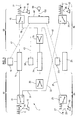
- the optical switching node 1 comprises a combination of two reconfigurable insertion / extraction (ROADM) multiplexers based on wavelength blocking modules.
- ROADM reconfigurable insertion / extraction
- Such a node may be used, for example, to process two optical flows going in two opposite directions in a ring network or the like.
- the dashes represent optical links, for example optical fibers, waveguides, integrated optics or the like, and the dashed lines represent control links, for example electrical or other.
- a first ROADM has an input port 11, an output port 17, a wavelength blocking module 14, an input optical section 91 connecting the port of FIG. input 11 to the input of the module 14, an optical output section 93 connecting the output of the module 14 to the output port 17, an extraction module 12 connected to the input section 91 by a coupler 18 to collect a fraction of the input optical signal and an insertion module 16 connected to the output section 93 by an optical combiner 19.
- a second ROADM has an input port 21, an output port 27, a wavelength blocking module 24, an input optical section 92 connecting the input port 21 to the input of the module 24, a section optical output 94 connecting the output of the module 24 to the output port 27, an extraction module 22 connected to the input section 92 by a coupler 28 to take a fraction of the input optical signal and an insertion module
- the extraction module 12, 22 is used to extract selected optical channels from the corresponding input optical signal.
- the insertion module 16, 26 is used to add optical channels to the optical signal coming out of the wavelength blocking module 14, 24.
- the wavelength blocking module 14, 24 serves to select channels to be transmitted in the corresponding input optical signal, to perform an amplitude optimization on these channels and to block the channels of the input signal which are not to be transmitted.
- the spectral optimization may be channel equalization or channel balancing according to predefined amplitude ratios, for example depending on the spectral response of the optical amplifiers present in the node.
- the node 1 comprises an additional wavelength blocking module 34 which is arranged so that it can be selectively substituted for each of the modules 14 and 24 to process their signal entry level.
- the wavelength-blocking module 34 has optical links connected to the first ROADM by couplers, combiners and / or switches bypassing the module 14 and optical links connected to the second ROADM by couplers, combiners and / or 24. More precisely, an input of the module 34 is connected to a combiner 1 ⁇ type 1 33 and an output of the module 34 is connected to a coupler 35 type 1x2. Since the first ROADM, an input line 31 extends between a selector switch 13 of type 1 ⁇ 2 interposed on the input section 91 and the combiner 33.
- an input line 32 is extends between a selector switch 23 of type 1 ⁇ 2 interposed on the input section 92 and the combiner 33.
- an output line 36 joins the output section 93 at a selective switch 15 of the type 1x2 and an output line 37 joins the output section 94 at a 1x2 selective switch.
- the selective switches 13 and 15 are positioned in a state where the module 14 (respectively 24) is in use.
- the first ROADM (respectively second) sends no signal to and receives no signal from the module 34.
- node 1 The control part of node 1 is now described.
- the three modules 14, 24 and 34 are assumed to be identical.
- the block 10, 20 or 30 denotes a low level controller, which can generally be packaged unitarily with the corresponding optical matrix.
- the controllers 10, 20 and 30 are connected to a node controller 40 by data links 41, 42 and 43.
- the module 34 In a normal operating state of the node, the module 34 is configured in a waiting state and is not used to process the traffic.
- the routing of the channels from the input port 1 (respectively 21) to the output port 17 (respectively 27) is essentially performed by the module 14 (respectively 24) according to instructions provided by the node controller 40 to the controller low level 10 (respectively 20).
- the node controller 40 has links 100 with external devices 99, for example a network management system and / or other node controllers.
- a general function of a switching state determination module 61 is to define the switching states in which the modules 14, 24 and 34 must be configured. at a given moment.
- the module 61 cooperates with a routing and signaling module 62, an optical monitoring module 64 and a protection management module 66.
- the module 62 is able to implement methods known in the field of routing and signaling in WDM networks.
- the module 62 controls the transmission and reception of the signaling instructions relating to the connections to be established, modified or deleted, as indicated by the arrow 63.
- the optical surveillance module 64 receives measurement information obtained by sensors (not shown) in FIG.
- the protection management module 66 detects situations of failure and controls the initiation and implementation of the protection of the modules 14 and 24.
- An interface module 70 controls the exchange of data and instructions with the low level controllers in appropriate formats or languages. More specifically, it comprises an interface 71 communicating with the controller 10 as indicated by the arrow 81, an interface 72 communicating with the controller 20 as indicated by the arrow 82 and an interface 73 communicating with the controller 30 as indicated by the arrow 83.
- the low level controller 10, 20 or 30 is designed to perform at least the step of translating a switching state to be achieved into control signals for the adjustable or switchable components of the optical matrix, namely for controlling the components optical so as to place the optical matrix in a desired switching state.
- the switching state to be reached here is defined by control instructions received by the low level controller 10, 20 or 30 from the node controller 40. Protocols suitable for communicating with the low level controller are for example Simple Network Management Protocol or Command Line Interface or lower level languages.
- the low level controller is able to calculate the state transitions to be made by the optical components, if any, and to transmit corresponding driving electrical signals to the optical components.
- the low level controller can be implemented in the form of a programmable electronic controller 74, visible in FIG. 3, essentially including a microprocessor 75, a memory 76, input / output interfaces 77, by example of the serial port type, control circuits 79 and a bus network 78 interconnecting these components.
- the control circuits 79 comprise the power electronics and the digital-to-analog converters for producing the actual driving signals, as indicated by the arrow 80.
- the microprocessor 75 and the memory 76 comprise the hardware and software means for determining, in according to the instructions defining a switching state to be achieved, the state transitions to be performed by the optical components.
- the switching state determination module 61 continuously calculates the switching states of the wavelength blockers 14 and 24 as a function of the connections to establish and signal levels to adjust.
- the node is adapted to a grid of wavelength channels.
- the wavelength blocker can assume a blocked state (designated by BLC in FIG. 2) or a conducting state with an adjustable attenuation in a predefined range, for example between 0 and -20 dB.
- BLC blocked state
- microactuator means here an elementary component or an elementary portion of controllable optical component for processing an elementary optical signal according to the granularity of the optical matrix, for example a wavelength channel.
- a microactuator may include a MEMS microelectromechanical device, a liquid crystal cell or other components.
- Wavelength blockers and wavelength selective switches based on MEMS microactuators are for example available from JDS Uniphase Corp. and Metconnex Canada Inc.
- Wavelength blockers and wavelength selective switches based on liquid crystal microactuators are for example available from Engana Pty Ltd, Australia.
- the instructions defining a state of switching to be reached can for example be transmitted through the interfaces 71, 72 or 73 and 77 in the form of a series of information including, for each microactuator to be reconfigured, a number or identifier of the microactuator or the corresponding wavelength channel, and the switching state to be achieved.
- These instructions are advantageously provided in the form of a list or an array of information arranged by microactuator or by wavelength channel.
- the module 61 has access to updated information defining the wavelengths that are received and processed by a ROADM at a given time.
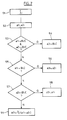
- the switching state determination module 61 also continuously calculates a standby switching state for the protection wavelength blocker 34. For this, the method illustrated in FIG. 2 is applied.
- a channel ⁇ i is selected from among the wavelength channels which are processed by the two wavelength blockers 14 and 24.
- a channel of wavelength ⁇ i is said to be common to both blockers of the wavelengths. wavelengths 14 and 24 when both blockers receive optical signals including this length wave. The data carried by this channel may be different in the two blockers.
- the switching states of the two wavelength blockers 14 and 24 for this channel designated a1i and a2i respectively, are read in a memory of the controller 40.
- step 54 the wait state for this channel, designated a3i, is set to the locked value BLC. If not, in step 55, it is tested whether the first module to be protected 14 blocks this channel. If so, in step 56, the waiting state for this channel is set to the state value of the other module to be protected 24, a2i, which is a passing value with a certain level of mitigation. If not, in step 57, it is tested whether the second module to be protected 24 blocks this channel. If so, in step 58, the waiting state for this channel is set to the state value of the other module to be protected 14, a1i, which is a passing value with a certain level of mitigation.
- the waiting state for this channel is set to the average value of the two modules to be protected 14 and 24, namely a passing value with an attenuation level which is the average of the attenuation levels of the two modules to be protected.
- the waiting state a3i is set for one channel, the method resumes in step 51 for another common channel if any remain.
- Table 1 gives an example of the waiting state obtained according to this method from two switching states for the channels ⁇ 1 to ⁇ 4.
- Table 1 Example of switching states of the wavelength blockers of FIG. 1. X means that this wavelength is not received by the blocker.
- This standby switching state constitutes the configuration from which the reconfiguration to any of the current switching states of the modules to be protected is statistically the fastest. Indeed, from the average attenuation level a3i obtained in step 59, the amplitude of the state transition of the corresponding microactuator to the attenuation level a1i or a2i is minimized.
- the state transition of a microactuator from the on state obtained at step 54 or 56 to the blocking state BLC, if any is generally faster than the inverse transition. For example, in an MEMS-based optical array, micromirrors must be stabilized in an on state, slowing down the transition to the on state.
- the method of FIG. 2 can be adapted in several ways to a 1: N protection scheme with N> 2. For example, if the switching states of the N modules to be protected for the common channel ⁇ i are blocked, the waiting state is blocked, otherwise the waiting state is a passing state whose attenuation level is the average attenuation levels of the modules to be protected which are not blocked.
- the switching states determined by the module 61 are transmitted as often as necessary to the low level controllers 10, 20 and 30 respectively, which correspondingly configure the optical matrices.
- the wait state is recalculated and communicated to the blocker 34 whenever one of the blockers to be protected 14 and 24 is reconfigured for at least one channel.
- the protection blocker 34 is permanently in a waiting state that statistically optimizes the reconfiguration time to the switching state of any of the modules to be protected.
- the protection management module 66 activates the protection by transmitting reconfiguration instructions to the controller 30. These instructions cause a reconfiguration of the blocker 34 in a switching state equivalent to the switching state of the module 14.
- the module 66 also controls the switches 13 and 15 to redirect the input signal of the blocker 14 to the blocker 34 and connect the output of the blocker 34 to the output of the first ROADM. Selective switches 13 and 15 (respectively 23 and 25) are controlled to switch simultaneously.
- the module 66 can detect a situation requiring to activate the protection in several ways.
- a protection command may be transmitted by a signaling message, as indicated by the arrow 69, for example from a network management system.
- An alert signal may also be transmitted by the optical surveillance module 64, as indicated by the arrow 68, or directly by a module to be protected having an integrated fault detection function, as indicated by the arrow 67.
- a wavelength blocker includes, for example, a channel monitoring device able to measure characteristics of the wavelength channels, for example the power, at different points of the blocker, for example ports, and a logical unit capable of to detect an abnormal state from these measurements, for example a loss of signal, and to produce a corresponding warning signal.
- the blocker 34 is functionally substituted for the failed module 14 to restore the service at the port 17. This recovery must be performed as quickly as possible.
- the wait state in which the shared protection module is preconfigured helps to speed up this recovery.
- the node controller 40 may transmit corresponding instructions to the low level controller 30 when it activates the protection.
- the controller 40 sends for it corresponding instructions for updating, periodically or whenever a module to protect is reconfigured.
- the controller 30 only has to read this information in its local memory when the protection must be activated.
- the controller 30 can also, in this case, precalculate and store the characteristics of the control signals that will be used, if necessary, when activating the protection.
- the controller 40 detects or is informed of a fault, it is sufficient for it to transmit to the low level controller 30 a protection command designating the faulty module. Due to the lower amount of data at transmit and / or precalculations performed, the reconfiguration of the protection module can be even faster.
- a wait state can be defined and used correspondingly for a shared protection scheme 1: N with any positive integer N ⁇ 2, preferably without additional traffic in the protection module.
- N any positive integer
- N ⁇ 2 preferably without additional traffic in the protection module.
- the architecture of FIG. 1 easily adapts to N> 2 using a combiner 33 and a coupler 35 of type 1 ⁇ N.
- a waiting state can be defined and used correspondingly in switching nodes of any degree and any architecture.
- Figure 1 can not be considered as limiting in this respect.
- the node controller 40 does not handle the gain control and transmits to the wavelength blockers configuration and reconfiguration instructions which take only two values for each channel, namely, on-state or blocked state.
- the method of FIG. 2 can be adapted to such a case, wherein the switching state for a wavelength channel is defined binary, i.e. either on or off.
- the waiting switching state a3i is set to the passing value without additional testing.
- the gain control can be individually managed by each low level controller from the measurements of the optical signals taken in the blocker.
- the low level controller 30 may apply a predefined average gain.
- the spectral optimization function managed by the low level controller 30 is implemented once an optical signal is actually present in the protection module, that is to say when the protection is activated.
- wavelength blockers Although the above embodiments refer to wavelength blockers, one skilled in the art will recognize that the same control methods can be applied in other types of wavelength processing modules having a greater or smaller number of ports, a greater or lesser number of different configuration states and more or less rich functionalities than the wavelength blockers, for example the wavelength selection switches (WSS) ). Still other examples of wavelength processing modules are simpler optical switching matrices, able to switch on one or more ports. output of the wavelength channels that they receive separately on input ports, without integrating a function of demultiplexing the channels.
- WSS wavelength selection switches
- the waiting state of the protection module for a wavelength channel can be calculated according to the selectable port to which this channel is directed in each module to be protected, and possibly depending on the respective gain levels. For example, if a channel is passed to a selectable port by the first module to be protected and passed to another port selectable by the second module to be protected, the waiting state for that channel may include an intermediate orientation of the corresponding micromirror in the protection module, for optimizing the switching time to one or the other of the two aforementioned selectable ports.
- wavelength processing module equipment capable of performing one or more treatments, such as pass, block, attenuate, amplify or polarize, on one or more wavelength channels.
- equipment is capable of processing optical signals with a granularity that may be a channel of individual wavelength or greater granularity, for example a group of channels, a spectral band, an optical fiber or the like. Note that, in the case of higher granularity, a configuration or switching state for an optical signal including a plurality of channels implicitly defines a configuration or switching state for any one wavelength channel of the plurality .
- the configuration state for a wavelength channel designates the physical configuration of the one or more elements of a processing module that affect the nature and / or the parameters of a processing undergone by this wavelength channel in the module.
- the logical relationship between a command addressed to a wavelength processing module and a wavelength channel may be direct, for example when a control instruction explicitly designates one or more wavelength channels to be affected by this command. This relation can also be indirect, for example when a command is intended to configure a particular hardware element of the processing module and that this hardware element is responsible for processing a particular optical signal containing that channel.
- controllers 10, 20, 30 and 40 and the network management system 99 can be made in different forms, unitarily or distributed, by means of hardware and / or software components.
- Hardware components that can be used are ASIC specific integrated circuits, FPGA programmable matrices or microprocessors.
- Software components can be written in different programming languages, for example C, C ++, Java or VHDL. This list is not exhaustive.
- node controller 40 and the low level controller 10, 20 or 30 could be performed more centrally, for example in a single controller, or could be distributed differently between a plurality of controllers.
- the preferred architecture described is not limiting in this regard.
- a network management system may be hardware equipment, for example a microcomputer, a workstation, a device connected to the Internet or any other dedicated or general purpose communication device.
- Software programs executed by this system perform network management functions to control network elements.
Landscapes
- Engineering & Computer Science (AREA)
- Computer Networks & Wireless Communication (AREA)
- Signal Processing (AREA)
- Optical Communication System (AREA)
- Semiconductor Lasers (AREA)
Applications Claiming Priority (1)
| Application Number | Priority Date | Filing Date | Title |
|---|---|---|---|
| FR0653827A FR2906045B1 (fr) | 2006-09-20 | 2006-09-20 | Procede de commande pour un module de protection partage et dispositif de traitement de longueurs d'ondes optiques |
Publications (2)
| Publication Number | Publication Date |
|---|---|
| EP1906574A1 true EP1906574A1 (de) | 2008-04-02 |
| EP1906574B1 EP1906574B1 (de) | 2011-04-13 |
Family
ID=37606939
Family Applications (1)
| Application Number | Title | Priority Date | Filing Date |
|---|---|---|---|
| EP07116724A Ceased EP1906574B1 (de) | 2006-09-20 | 2007-09-19 | Verfahren zur Steuerung eines gemeinsamen Schutzmoduls und Vorrichtung zur Verarbeitung von optischen Wellenlängen |
Country Status (4)
| Country | Link |
|---|---|
| EP (1) | EP1906574B1 (de) |
| AT (1) | ATE505866T1 (de) |
| DE (1) | DE602007013848D1 (de) |
| FR (1) | FR2906045B1 (de) |
Citations (4)
| Publication number | Priority date | Publication date | Assignee | Title |
|---|---|---|---|---|
| WO2000057583A1 (en) * | 1999-03-24 | 2000-09-28 | Tellium, Inc. | Optical matrix protection system |
| EP1111954A2 (de) * | 1999-12-22 | 2001-06-27 | Nortel Networks Limited | Verteile Optische Schaltvorrichtung |
| WO2001056211A1 (en) * | 2000-01-25 | 2001-08-02 | Corning Incorporated | Optical protection system for liquid crystal switches |
| WO2002075371A2 (en) * | 2001-03-20 | 2002-09-26 | Corning, Inc. | Dwdm ring networks using wavelength selected switches |
-
2006
- 2006-09-20 FR FR0653827A patent/FR2906045B1/fr not_active Expired - Fee Related
-
2007
- 2007-09-19 DE DE602007013848T patent/DE602007013848D1/de active Active
- 2007-09-19 EP EP07116724A patent/EP1906574B1/de not_active Ceased
- 2007-09-19 AT AT07116724T patent/ATE505866T1/de not_active IP Right Cessation
Patent Citations (4)
| Publication number | Priority date | Publication date | Assignee | Title |
|---|---|---|---|---|
| WO2000057583A1 (en) * | 1999-03-24 | 2000-09-28 | Tellium, Inc. | Optical matrix protection system |
| EP1111954A2 (de) * | 1999-12-22 | 2001-06-27 | Nortel Networks Limited | Verteile Optische Schaltvorrichtung |
| WO2001056211A1 (en) * | 2000-01-25 | 2001-08-02 | Corning Incorporated | Optical protection system for liquid crystal switches |
| WO2002075371A2 (en) * | 2001-03-20 | 2002-09-26 | Corning, Inc. | Dwdm ring networks using wavelength selected switches |
Non-Patent Citations (1)
| Title |
|---|
| RHEE J-K ET AL: "A BROADCAST-AND-SELECT OADM OPTICAL NETWORK WITH DEDICATED OPTICAL-CHANNEL PROTECTION", JOURNAL OF LIGHTWAVE TECHNOLOGY, IEEE SERVICE CENTER, NEW YORK, NY, US, vol. 21, no. 1, January 2003 (2003-01-01), pages 25 - 31, XP001228593, ISSN: 0733-8724 * |
Also Published As
| Publication number | Publication date |
|---|---|
| DE602007013848D1 (de) | 2011-05-26 |
| FR2906045B1 (fr) | 2008-10-31 |
| ATE505866T1 (de) | 2011-04-15 |
| EP1906574B1 (de) | 2011-04-13 |
| FR2906045A1 (fr) | 2008-03-21 |
Similar Documents
| Publication | Publication Date | Title |
|---|---|---|
| EP1879308B1 (de) | Verfahren und Vorrichtung zur Überwachung von optischen Verbindungen in einem transparenten optischen Netzwerk | |
| US9941955B2 (en) | Optical network monitoring and protection using a phased array switching engine | |
| JP4654560B2 (ja) | 光出力制御装置、光出力制御方法および光出力制御プログラム | |
| CN1262085C (zh) | 光信号电平控制方法和装置 | |
| US20040131353A1 (en) | Method and apparatus providing transient control in optical add-drop nodes | |
| JP2006518132A (ja) | 光ネットワークの保護スイッチング・アーキテクチャ | |
| FR2849305A1 (fr) | Procede et dispositif perfectionnes de controle de la puissance delivree en sortie d'un noeud d'un reseau optique a commutation de bandes de longueurs d'onde | |
| EP1906574B1 (de) | Verfahren zur Steuerung eines gemeinsamen Schutzmoduls und Vorrichtung zur Verarbeitung von optischen Wellenlängen | |
| FR2893718A1 (fr) | Dispositif de commutation optique entre des lignes optiques amont et aval, a adjonction de signature de noeud pour le suivi des chemins optiques de connexion | |
| CA2414043A1 (en) | Shared optical ring protection in a multi-fiber ring | |
| EP1901099B1 (de) | Schaltmodul für optische Wellenlängen | |
| JP5023021B2 (ja) | 光分岐挿入多重化装置、及び光レベル調整方法 | |
| EP0982891B1 (de) | Vorrichtung zum Ein-Ausfügen eines optischen Wellenlängenmultiplexsignales | |
| EP2073566B1 (de) | Verfahren zur Herstellung einer Verbindung zur Rückgewinnung in einem optischen Netz | |
| EP2160045B1 (de) | Knoten zur Kommunikation von optischen Paketen | |
| US6556766B2 (en) | MEMS see-saw array for dynamic gain equalization of DWDM systems | |
| EP1966581B1 (de) | Verfahren zum messen der differentialgruppenverzögerung einer optischen verknüpfung | |
| JP4851553B2 (ja) | 光スイッチとその制御方法 | |
| EP1879309A1 (de) | Verfahren und Vorrichtung zur Überwachung von Lichtverbindungswegen für ein transparentes optisches Netz | |
| EP4489328A1 (de) | Verfahren und vorrichtung zur verwaltung eines betriebsfehlers einer laserdiode | |
| EP1804407B1 (de) | Accessknoten für optisches Ringnetzwerk | |
| EP1453227B1 (de) | Dynamische Steuerung des Qualitätsverlustes von optischen Signalen in einem transparenten optischen Kommunikationsnetzwerk | |
| EP2007049B1 (de) | Vorrichtung zur Übertragung optischer Signale mit unterschiedlichen Datenraten | |
| JP2012227838A (ja) | 光伝送装置 | |
| JP2011166840A (ja) | 光伝送装置 |
Legal Events
| Date | Code | Title | Description |
|---|---|---|---|
| PUAI | Public reference made under article 153(3) epc to a published international application that has entered the european phase |
Free format text: ORIGINAL CODE: 0009012 |
|
| AK | Designated contracting states |
Kind code of ref document: A1 Designated state(s): AT BE BG CH CY CZ DE DK EE ES FI FR GB GR HU IE IS IT LI LT LU LV MC MT NL PL PT RO SE SI SK TR |
|
| AX | Request for extension of the european patent |
Extension state: AL BA HR MK YU |
|
| 17P | Request for examination filed |
Effective date: 20081002 |
|
| AKX | Designation fees paid |
Designated state(s): AT BE BG CH CY CZ DE DK EE ES FI FR GB GR HU IE IS IT LI LT LU LV MC MT NL PL PT RO SE SI SK TR |
|
| 17Q | First examination report despatched |
Effective date: 20091103 |
|
| R17C | First examination report despatched (corrected) |
Effective date: 20100119 |
|
| GRAP | Despatch of communication of intention to grant a patent |
Free format text: ORIGINAL CODE: EPIDOSNIGR1 |
|
| GRAS | Grant fee paid |
Free format text: ORIGINAL CODE: EPIDOSNIGR3 |
|
| GRAA | (expected) grant |
Free format text: ORIGINAL CODE: 0009210 |
|
| AK | Designated contracting states |
Kind code of ref document: B1 Designated state(s): AT BE BG CH CY CZ DE DK EE ES FI FR GB GR HU IE IS IT LI LT LU LV MC MT NL PL PT RO SE SI SK TR |
|
| REG | Reference to a national code |
Ref country code: GB Ref legal event code: FG4D Free format text: NOT ENGLISH |
|
| REG | Reference to a national code |
Ref country code: CH Ref legal event code: EP |
|
| REG | Reference to a national code |
Ref country code: IE Ref legal event code: FG4D Free format text: LANGUAGE OF EP DOCUMENT: FRENCH |
|
| REF | Corresponds to: |
Ref document number: 602007013848 Country of ref document: DE Date of ref document: 20110526 Kind code of ref document: P |
|
| REG | Reference to a national code |
Ref country code: DE Ref legal event code: R096 Ref document number: 602007013848 Country of ref document: DE Effective date: 20110526 |
|
| REG | Reference to a national code |
Ref country code: NL Ref legal event code: VDEP Effective date: 20110413 |
|
| LTIE | Lt: invalidation of european patent or patent extension |
Effective date: 20110413 |
|
| PG25 | Lapsed in a contracting state [announced via postgrant information from national office to epo] |
Ref country code: PT Free format text: LAPSE BECAUSE OF FAILURE TO SUBMIT A TRANSLATION OF THE DESCRIPTION OR TO PAY THE FEE WITHIN THE PRESCRIBED TIME-LIMIT Effective date: 20110816 Ref country code: SE Free format text: LAPSE BECAUSE OF FAILURE TO SUBMIT A TRANSLATION OF THE DESCRIPTION OR TO PAY THE FEE WITHIN THE PRESCRIBED TIME-LIMIT Effective date: 20110413 Ref country code: LT Free format text: LAPSE BECAUSE OF FAILURE TO SUBMIT A TRANSLATION OF THE DESCRIPTION OR TO PAY THE FEE WITHIN THE PRESCRIBED TIME-LIMIT Effective date: 20110413 |
|
| REG | Reference to a national code |
Ref country code: IE Ref legal event code: FD4D |
|
| PG25 | Lapsed in a contracting state [announced via postgrant information from national office to epo] |
Ref country code: LV Free format text: LAPSE BECAUSE OF FAILURE TO SUBMIT A TRANSLATION OF THE DESCRIPTION OR TO PAY THE FEE WITHIN THE PRESCRIBED TIME-LIMIT Effective date: 20110413 Ref country code: IS Free format text: LAPSE BECAUSE OF FAILURE TO SUBMIT A TRANSLATION OF THE DESCRIPTION OR TO PAY THE FEE WITHIN THE PRESCRIBED TIME-LIMIT Effective date: 20110813 Ref country code: GR Free format text: LAPSE BECAUSE OF FAILURE TO SUBMIT A TRANSLATION OF THE DESCRIPTION OR TO PAY THE FEE WITHIN THE PRESCRIBED TIME-LIMIT Effective date: 20110714 Ref country code: ES Free format text: LAPSE BECAUSE OF FAILURE TO SUBMIT A TRANSLATION OF THE DESCRIPTION OR TO PAY THE FEE WITHIN THE PRESCRIBED TIME-LIMIT Effective date: 20110724 Ref country code: CY Free format text: LAPSE BECAUSE OF FAILURE TO SUBMIT A TRANSLATION OF THE DESCRIPTION OR TO PAY THE FEE WITHIN THE PRESCRIBED TIME-LIMIT Effective date: 20110413 Ref country code: SI Free format text: LAPSE BECAUSE OF FAILURE TO SUBMIT A TRANSLATION OF THE DESCRIPTION OR TO PAY THE FEE WITHIN THE PRESCRIBED TIME-LIMIT Effective date: 20110413 Ref country code: AT Free format text: LAPSE BECAUSE OF FAILURE TO SUBMIT A TRANSLATION OF THE DESCRIPTION OR TO PAY THE FEE WITHIN THE PRESCRIBED TIME-LIMIT Effective date: 20110413 Ref country code: FI Free format text: LAPSE BECAUSE OF FAILURE TO SUBMIT A TRANSLATION OF THE DESCRIPTION OR TO PAY THE FEE WITHIN THE PRESCRIBED TIME-LIMIT Effective date: 20110413 |
|
| PG25 | Lapsed in a contracting state [announced via postgrant information from national office to epo] |
Ref country code: NL Free format text: LAPSE BECAUSE OF FAILURE TO SUBMIT A TRANSLATION OF THE DESCRIPTION OR TO PAY THE FEE WITHIN THE PRESCRIBED TIME-LIMIT Effective date: 20110413 |
|
| PG25 | Lapsed in a contracting state [announced via postgrant information from national office to epo] |
Ref country code: EE Free format text: LAPSE BECAUSE OF FAILURE TO SUBMIT A TRANSLATION OF THE DESCRIPTION OR TO PAY THE FEE WITHIN THE PRESCRIBED TIME-LIMIT Effective date: 20110413 Ref country code: IE Free format text: LAPSE BECAUSE OF FAILURE TO SUBMIT A TRANSLATION OF THE DESCRIPTION OR TO PAY THE FEE WITHIN THE PRESCRIBED TIME-LIMIT Effective date: 20110413 Ref country code: CZ Free format text: LAPSE BECAUSE OF FAILURE TO SUBMIT A TRANSLATION OF THE DESCRIPTION OR TO PAY THE FEE WITHIN THE PRESCRIBED TIME-LIMIT Effective date: 20110413 |
|
| PLBE | No opposition filed within time limit |
Free format text: ORIGINAL CODE: 0009261 |
|
| STAA | Information on the status of an ep patent application or granted ep patent |
Free format text: STATUS: NO OPPOSITION FILED WITHIN TIME LIMIT |
|
| RAP2 | Party data changed (patent owner data changed or rights of a patent transferred) |
Owner name: ALCATEL LUCENT |
|
| PG25 | Lapsed in a contracting state [announced via postgrant information from national office to epo] |
Ref country code: SK Free format text: LAPSE BECAUSE OF FAILURE TO SUBMIT A TRANSLATION OF THE DESCRIPTION OR TO PAY THE FEE WITHIN THE PRESCRIBED TIME-LIMIT Effective date: 20110413 Ref country code: DK Free format text: LAPSE BECAUSE OF FAILURE TO SUBMIT A TRANSLATION OF THE DESCRIPTION OR TO PAY THE FEE WITHIN THE PRESCRIBED TIME-LIMIT Effective date: 20110413 Ref country code: PL Free format text: LAPSE BECAUSE OF FAILURE TO SUBMIT A TRANSLATION OF THE DESCRIPTION OR TO PAY THE FEE WITHIN THE PRESCRIBED TIME-LIMIT Effective date: 20110413 Ref country code: RO Free format text: LAPSE BECAUSE OF FAILURE TO SUBMIT A TRANSLATION OF THE DESCRIPTION OR TO PAY THE FEE WITHIN THE PRESCRIBED TIME-LIMIT Effective date: 20110413 |
|
| REG | Reference to a national code |
Ref country code: CH Ref legal event code: PCOW Free format text: ALCATEL LUCENT;3, AVENUE OCTAVE GREARD;75007 PARIS (FR) |
|
| 26N | No opposition filed |
Effective date: 20120116 |
|
| BERE | Be: lapsed |
Owner name: ALCATEL LUCENT Effective date: 20110930 |
|
| PG25 | Lapsed in a contracting state [announced via postgrant information from national office to epo] |
Ref country code: MC Free format text: LAPSE BECAUSE OF NON-PAYMENT OF DUE FEES Effective date: 20110930 |
|
| REG | Reference to a national code |
Ref country code: CH Ref legal event code: PL |
|
| REG | Reference to a national code |
Ref country code: DE Ref legal event code: R097 Ref document number: 602007013848 Country of ref document: DE Effective date: 20120116 |
|
| PG25 | Lapsed in a contracting state [announced via postgrant information from national office to epo] |
Ref country code: IT Free format text: LAPSE BECAUSE OF FAILURE TO SUBMIT A TRANSLATION OF THE DESCRIPTION OR TO PAY THE FEE WITHIN THE PRESCRIBED TIME-LIMIT Effective date: 20110413 |
|
| PG25 | Lapsed in a contracting state [announced via postgrant information from national office to epo] |
Ref country code: BE Free format text: LAPSE BECAUSE OF NON-PAYMENT OF DUE FEES Effective date: 20110930 |
|
| PG25 | Lapsed in a contracting state [announced via postgrant information from national office to epo] |
Ref country code: LI Free format text: LAPSE BECAUSE OF NON-PAYMENT OF DUE FEES Effective date: 20110930 Ref country code: CH Free format text: LAPSE BECAUSE OF NON-PAYMENT OF DUE FEES Effective date: 20110930 |
|
| PG25 | Lapsed in a contracting state [announced via postgrant information from national office to epo] |
Ref country code: MT Free format text: LAPSE BECAUSE OF FAILURE TO SUBMIT A TRANSLATION OF THE DESCRIPTION OR TO PAY THE FEE WITHIN THE PRESCRIBED TIME-LIMIT Effective date: 20110413 |
|
| PG25 | Lapsed in a contracting state [announced via postgrant information from national office to epo] |
Ref country code: LU Free format text: LAPSE BECAUSE OF NON-PAYMENT OF DUE FEES Effective date: 20110919 |
|
| PG25 | Lapsed in a contracting state [announced via postgrant information from national office to epo] |
Ref country code: BG Free format text: LAPSE BECAUSE OF FAILURE TO SUBMIT A TRANSLATION OF THE DESCRIPTION OR TO PAY THE FEE WITHIN THE PRESCRIBED TIME-LIMIT Effective date: 20110713 |
|
| PG25 | Lapsed in a contracting state [announced via postgrant information from national office to epo] |
Ref country code: TR Free format text: LAPSE BECAUSE OF FAILURE TO SUBMIT A TRANSLATION OF THE DESCRIPTION OR TO PAY THE FEE WITHIN THE PRESCRIBED TIME-LIMIT Effective date: 20110413 |
|
| PG25 | Lapsed in a contracting state [announced via postgrant information from national office to epo] |
Ref country code: HU Free format text: LAPSE BECAUSE OF FAILURE TO SUBMIT A TRANSLATION OF THE DESCRIPTION OR TO PAY THE FEE WITHIN THE PRESCRIBED TIME-LIMIT Effective date: 20110413 |
|
| REG | Reference to a national code |
Ref country code: FR Ref legal event code: GC Effective date: 20131018 |
|
| REG | Reference to a national code |
Ref country code: FR Ref legal event code: RG Effective date: 20141016 |
|
| REG | Reference to a national code |
Ref country code: FR Ref legal event code: PLFP Year of fee payment: 9 |
|
| REG | Reference to a national code |
Ref country code: FR Ref legal event code: PLFP Year of fee payment: 10 |
|
| REG | Reference to a national code |
Ref country code: FR Ref legal event code: PLFP Year of fee payment: 11 |
|
| PGFP | Annual fee paid to national office [announced via postgrant information from national office to epo] |
Ref country code: GB Payment date: 20180327 Year of fee payment: 11 |
|
| PGFP | Annual fee paid to national office [announced via postgrant information from national office to epo] |
Ref country code: FR Payment date: 20180329 Year of fee payment: 11 |
|
| PGFP | Annual fee paid to national office [announced via postgrant information from national office to epo] |
Ref country code: DE Payment date: 20180328 Year of fee payment: 11 |
|
| REG | Reference to a national code |
Ref country code: DE Ref legal event code: R119 Ref document number: 602007013848 Country of ref document: DE |
|
| GBPC | Gb: european patent ceased through non-payment of renewal fee |
Effective date: 20180919 |
|
| PG25 | Lapsed in a contracting state [announced via postgrant information from national office to epo] |
Ref country code: DE Free format text: LAPSE BECAUSE OF NON-PAYMENT OF DUE FEES Effective date: 20190402 |
|
| PG25 | Lapsed in a contracting state [announced via postgrant information from national office to epo] |
Ref country code: FR Free format text: LAPSE BECAUSE OF NON-PAYMENT OF DUE FEES Effective date: 20180930 |
|
| PG25 | Lapsed in a contracting state [announced via postgrant information from national office to epo] |
Ref country code: GB Free format text: LAPSE BECAUSE OF NON-PAYMENT OF DUE FEES Effective date: 20180919 |
|
| REG | Reference to a national code |
Ref country code: DE Ref legal event code: R081 Ref document number: 602007013848 Country of ref document: DE Owner name: WSOU INVESTMENTS, LLC, LOS ANGELES, US Free format text: FORMER OWNER: ALCATEL LUCENT, PARIS, FR Ref country code: DE Ref legal event code: R082 Ref document number: 602007013848 Country of ref document: DE Representative=s name: BARKHOFF REIMANN VOSSIUS, DE |
|
| REG | Reference to a national code |
Ref country code: GB Ref legal event code: 732E Free format text: REGISTERED BETWEEN 20200827 AND 20200902 |