EP1909329A1 - Dispositif semi-conducteur - Google Patents
Dispositif semi-conducteur Download PDFInfo
- Publication number
- EP1909329A1 EP1909329A1 EP06729670A EP06729670A EP1909329A1 EP 1909329 A1 EP1909329 A1 EP 1909329A1 EP 06729670 A EP06729670 A EP 06729670A EP 06729670 A EP06729670 A EP 06729670A EP 1909329 A1 EP1909329 A1 EP 1909329A1
- Authority
- EP
- European Patent Office
- Prior art keywords
- semiconductor element
- base region
- region
- igbt
- electrode
- Prior art date
- Legal status (The legal status is an assumption and is not a legal conclusion. Google has not performed a legal analysis and makes no representation as to the accuracy of the status listed.)
- Granted
Links
Images


Classifications
-
- H—ELECTRICITY
- H10—SEMICONDUCTOR DEVICES; ELECTRIC SOLID-STATE DEVICES NOT OTHERWISE PROVIDED FOR
- H10D—INORGANIC ELECTRIC SEMICONDUCTOR DEVICES
- H10D12/00—Bipolar devices controlled by the field effect, e.g. insulated-gate bipolar transistors [IGBT]
-
- H—ELECTRICITY
- H10—SEMICONDUCTOR DEVICES; ELECTRIC SOLID-STATE DEVICES NOT OTHERWISE PROVIDED FOR
- H10W—GENERIC PACKAGES, INTERCONNECTIONS, CONNECTORS OR OTHER CONSTRUCTIONAL DETAILS OF DEVICES COVERED BY CLASS H10
- H10W90/00—Package configurations
- H10W90/811—Multiple chips on leadframes
-
- H—ELECTRICITY
- H10—SEMICONDUCTOR DEVICES; ELECTRIC SOLID-STATE DEVICES NOT OTHERWISE PROVIDED FOR
- H10D—INORGANIC ELECTRIC SEMICONDUCTOR DEVICES
- H10D12/00—Bipolar devices controlled by the field effect, e.g. insulated-gate bipolar transistors [IGBT]
- H10D12/411—Insulated-gate bipolar transistors [IGBT]
- H10D12/441—Vertical IGBTs
-
- H—ELECTRICITY
- H10—SEMICONDUCTOR DEVICES; ELECTRIC SOLID-STATE DEVICES NOT OTHERWISE PROVIDED FOR
- H10D—INORGANIC ELECTRIC SEMICONDUCTOR DEVICES
- H10D84/00—Integrated devices formed in or on semiconductor substrates that comprise only semiconducting layers, e.g. on Si wafers or on GaAs-on-Si wafers
-
- H—ELECTRICITY
- H10—SEMICONDUCTOR DEVICES; ELECTRIC SOLID-STATE DEVICES NOT OTHERWISE PROVIDED FOR
- H10D—INORGANIC ELECTRIC SEMICONDUCTOR DEVICES
- H10D99/00—Subject matter not provided for in other groups of this subclass
-
- H—ELECTRICITY
- H10—SEMICONDUCTOR DEVICES; ELECTRIC SOLID-STATE DEVICES NOT OTHERWISE PROVIDED FOR
- H10W—GENERIC PACKAGES, INTERCONNECTIONS, CONNECTORS OR OTHER CONSTRUCTIONAL DETAILS OF DEVICES COVERED BY CLASS H10
- H10W90/00—Package configurations
-
- H—ELECTRICITY
- H10—SEMICONDUCTOR DEVICES; ELECTRIC SOLID-STATE DEVICES NOT OTHERWISE PROVIDED FOR
- H10D—INORGANIC ELECTRIC SEMICONDUCTOR DEVICES
- H10D88/00—Three-dimensional [3D] integrated devices
-
- H—ELECTRICITY
- H10—SEMICONDUCTOR DEVICES; ELECTRIC SOLID-STATE DEVICES NOT OTHERWISE PROVIDED FOR
- H10W—GENERIC PACKAGES, INTERCONNECTIONS, CONNECTORS OR OTHER CONSTRUCTIONAL DETAILS OF DEVICES COVERED BY CLASS H10
- H10W72/00—Interconnections or connectors in packages
- H10W72/50—Bond wires
- H10W72/541—Dispositions of bond wires
- H10W72/5449—Dispositions of bond wires not being orthogonal to a side surface of the chip, e.g. fan-out arrangements
-
- H—ELECTRICITY
- H10—SEMICONDUCTOR DEVICES; ELECTRIC SOLID-STATE DEVICES NOT OTHERWISE PROVIDED FOR
- H10W—GENERIC PACKAGES, INTERCONNECTIONS, CONNECTORS OR OTHER CONSTRUCTIONAL DETAILS OF DEVICES COVERED BY CLASS H10
- H10W72/00—Interconnections or connectors in packages
- H10W72/50—Bond wires
- H10W72/551—Materials of bond wires
- H10W72/552—Materials of bond wires comprising metals or metalloids, e.g. silver
- H10W72/5524—Materials of bond wires comprising metals or metalloids, e.g. silver comprising aluminium [Al]
-
- H—ELECTRICITY
- H10—SEMICONDUCTOR DEVICES; ELECTRIC SOLID-STATE DEVICES NOT OTHERWISE PROVIDED FOR
- H10W—GENERIC PACKAGES, INTERCONNECTIONS, CONNECTORS OR OTHER CONSTRUCTIONAL DETAILS OF DEVICES COVERED BY CLASS H10
- H10W72/00—Interconnections or connectors in packages
- H10W72/851—Dispositions of multiple connectors or interconnections
- H10W72/874—On different surfaces
- H10W72/884—Die-attach connectors and bond wires
-
- H—ELECTRICITY
- H10—SEMICONDUCTOR DEVICES; ELECTRIC SOLID-STATE DEVICES NOT OTHERWISE PROVIDED FOR
- H10W—GENERIC PACKAGES, INTERCONNECTIONS, CONNECTORS OR OTHER CONSTRUCTIONAL DETAILS OF DEVICES COVERED BY CLASS H10
- H10W72/00—Interconnections or connectors in packages
- H10W72/90—Bond pads, in general
- H10W72/921—Structures or relative sizes of bond pads
- H10W72/926—Multiple bond pads having different sizes
-
- H—ELECTRICITY
- H10—SEMICONDUCTOR DEVICES; ELECTRIC SOLID-STATE DEVICES NOT OTHERWISE PROVIDED FOR
- H10W—GENERIC PACKAGES, INTERCONNECTIONS, CONNECTORS OR OTHER CONSTRUCTIONAL DETAILS OF DEVICES COVERED BY CLASS H10
- H10W72/00—Interconnections or connectors in packages
- H10W72/90—Bond pads, in general
- H10W72/931—Shapes of bond pads
- H10W72/932—Plan-view shape, i.e. in top view
-
- H—ELECTRICITY
- H10—SEMICONDUCTOR DEVICES; ELECTRIC SOLID-STATE DEVICES NOT OTHERWISE PROVIDED FOR
- H10W—GENERIC PACKAGES, INTERCONNECTIONS, CONNECTORS OR OTHER CONSTRUCTIONAL DETAILS OF DEVICES COVERED BY CLASS H10
- H10W74/00—Encapsulations, e.g. protective coatings
-
- H—ELECTRICITY
- H10—SEMICONDUCTOR DEVICES; ELECTRIC SOLID-STATE DEVICES NOT OTHERWISE PROVIDED FOR
- H10W—GENERIC PACKAGES, INTERCONNECTIONS, CONNECTORS OR OTHER CONSTRUCTIONAL DETAILS OF DEVICES COVERED BY CLASS H10
- H10W90/00—Package configurations
- H10W90/701—Package configurations characterised by the relative positions of pads or connectors relative to package parts
- H10W90/731—Package configurations characterised by the relative positions of pads or connectors relative to package parts of die-attach connectors
- H10W90/732—Package configurations characterised by the relative positions of pads or connectors relative to package parts of die-attach connectors between stacked chips
-
- H—ELECTRICITY
- H10—SEMICONDUCTOR DEVICES; ELECTRIC SOLID-STATE DEVICES NOT OTHERWISE PROVIDED FOR
- H10W—GENERIC PACKAGES, INTERCONNECTIONS, CONNECTORS OR OTHER CONSTRUCTIONAL DETAILS OF DEVICES COVERED BY CLASS H10
- H10W90/00—Package configurations
- H10W90/701—Package configurations characterised by the relative positions of pads or connectors relative to package parts
- H10W90/731—Package configurations characterised by the relative positions of pads or connectors relative to package parts of die-attach connectors
- H10W90/734—Package configurations characterised by the relative positions of pads or connectors relative to package parts of die-attach connectors between a chip and a stacked insulating package substrate, interposer or RDL
-
- H—ELECTRICITY
- H10—SEMICONDUCTOR DEVICES; ELECTRIC SOLID-STATE DEVICES NOT OTHERWISE PROVIDED FOR
- H10W—GENERIC PACKAGES, INTERCONNECTIONS, CONNECTORS OR OTHER CONSTRUCTIONAL DETAILS OF DEVICES COVERED BY CLASS H10
- H10W90/00—Package configurations
- H10W90/701—Package configurations characterised by the relative positions of pads or connectors relative to package parts
- H10W90/751—Package configurations characterised by the relative positions of pads or connectors relative to package parts of bond wires
- H10W90/753—Package configurations characterised by the relative positions of pads or connectors relative to package parts of bond wires between laterally-adjacent chips
-
- H—ELECTRICITY
- H10—SEMICONDUCTOR DEVICES; ELECTRIC SOLID-STATE DEVICES NOT OTHERWISE PROVIDED FOR
- H10W—GENERIC PACKAGES, INTERCONNECTIONS, CONNECTORS OR OTHER CONSTRUCTIONAL DETAILS OF DEVICES COVERED BY CLASS H10
- H10W90/00—Package configurations
- H10W90/701—Package configurations characterised by the relative positions of pads or connectors relative to package parts
- H10W90/751—Package configurations characterised by the relative positions of pads or connectors relative to package parts of bond wires
- H10W90/754—Package configurations characterised by the relative positions of pads or connectors relative to package parts of bond wires between a chip and a stacked insulating package substrate, interposer or RDL
-
- H—ELECTRICITY
- H10—SEMICONDUCTOR DEVICES; ELECTRIC SOLID-STATE DEVICES NOT OTHERWISE PROVIDED FOR
- H10W—GENERIC PACKAGES, INTERCONNECTIONS, CONNECTORS OR OTHER CONSTRUCTIONAL DETAILS OF DEVICES COVERED BY CLASS H10
- H10W90/00—Package configurations
- H10W90/701—Package configurations characterised by the relative positions of pads or connectors relative to package parts
- H10W90/751—Package configurations characterised by the relative positions of pads or connectors relative to package parts of bond wires
- H10W90/756—Package configurations characterised by the relative positions of pads or connectors relative to package parts of bond wires between a chip and a stacked lead frame, conducting package substrate or heat sink
Definitions
- the present invention relates to a semiconductor device including a plurality of layered semiconductor elements.
- Patent Publication 1 As a means for coping with electronic components having a smaller size in recent years, a semiconductor device has been used that uses a stacked multi structure in which switching elements are layered to constitute a bridge circuit.
- a semiconductor device using a stacked multi structure is known from the following Patent Publication 1 for example.
- an H-type bridge circuit using a power semiconductor element can be formed with an improved integration degree while decreasing an area occupied by a supporting plate.
- MOSFET MOS-type field effect transistor
- the chip size is increased to prevent a smaller size from being achieved.
- an insulated gate-type bipolar transistor (IGBT) that can realize a smaller chip size has been used.
- the use of the IGBT additionally requires an external diode to be mounted in an H-type bridge circuit. This has consequently prevented a smaller size from being achieved and has caused an increased product cost due to the external diode.
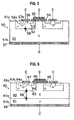
- MOSFET includes, as shown in FIG. 5 for example, a semiconductor substrate (50) including an N-type conductivity type drain region (51), a P-type conductivity type base region (52) formed on an upper face (51a) of a drain region (51), and an N-type conductivity type source region (53) formed on an upper face (52a) of a base region (52); a gate electrode (55) formed on an upper face (53a) of the source region (53) via a gate insulating film (54); a source electrode (56) formed on the base region (52) and an upper face (52a, 53a) of the source region (53); and a drain electrode (57) formed on a lower face (51b) of the drain region (51).
- the P-type conductivity type base region (52) and the N-type conductivity type drain region (51) have therebetween a diode (58) that can be used as an inner diode to be protected.
- the IGBT has, as shown in FIG. 6 , a semiconductor substrate (60) that has a P-type conductivity type collector region (61), a first base region (62) of N-type conductivity type that is formed on an upper face (61a) of the collector region (61), and a second base region (63) of P-type conductivity type that is formed on an upper face (62a) of the first base region (62), and an emitter region (64) of N-type conductivity type that is formed on an upper face (63a) of the second base region (63); a gate electrode (66) formed on an upper face (63a) of the second base region (63) via a gate insulating film (65); an emitter electrode (67) formed on an upper face (63a, 64a) of the second base region (63) and the emitter region (64); and a collector electrode (68) formed on a lower face (61b) of the collector region (61).
- a semiconductor substrate (60) that has a P-type conductivity type collector region (61), a first
- the IGBT is structured as shown in FIG. 6 so that a diode (69) is each formed between the second base region (63) of P-type conductivity type and the first base region (62) of N-type conductivity type and between the collector region (61) of P-type conductivity type and the first base region (62) of N-type conductivity type, respectively.
- the diodes (69) having reverse polarities are series-connected. This has caused a difficulty where this diode cannot be used as an inner diode for protection of transistor.
- an H-bridge circuit in which an output terminal is connected with a load having an induction component for example, a back electromotive force caused by the induction component of the load tends to be applied to the IGBT.
- each IGBT must be connected in parallel to the diode to bypass current in a reverse direction (surge current) caused by the electromotive force via the diode.
- Patent Publication 2 discloses an IGBT in which the center of a collector region has a cathode region having an opposite conductivity type and the upper part of the cathode region has a P-type conductivity type anode region to store a diode. According to the IGBT of Patent Publication 2, an external diode can be omitted and a semiconductor device having a stacked multi structure having layered IGBT can be formed.
- Patent Publication 1 International Publication Number WO 2005/018001
- Patent Publication 2 Japanese Laid-Open Publication No. H9-191110
- a semiconductor device of the present invention has a first semiconductor element and a second semiconductor element that is layered and fixed on the first semiconductor element.
- Each of the first semiconductor element and the second semiconductor element comprises: (i) a semiconductor substrate including a collector region of a first conductivity type (P/N), a first base region that has a second conductivity type (N/P) opposite to the first conductivity type and that is formed on an upper face of the collector region, a second base region that has the first conductivity type and that is formed to be adjacent to the first base region, and an emitter region that has the second conductivity type and that is formed to be adjacent to the second base region; (ii) a gate electrode formed on an upper face of the second base region via an insulating material; (iii) an emitter electrode formed on upper faces of the second base region and the emitter region; and (iv) a collector electrode formed on a lower face of the collector region.
- P/N first conductivity type
- N/P second conductivity type
- the first base region has a peripheral section in the vicinity of the side face of the semiconductor substrate.
- Each of the first semiconductor element and the second semiconductor element has a peripheral base region that has the first conductivity type and that is formed to be adjacent to a peripheral section of the first base region to form a diode and a diode electrode that is formed on an upper face of the peripheral section of the first base region.
- the diode electrode and the collector electrode of the first semiconductor element and the second semiconductor element are electrically connected, respectively.
- a back electromotive force due to an induction component of a load connected thereto causes reverse current (surge current) to be induced in a reverse direction from the emitter electrodes of the first semiconductor element and the second semiconductor element to the collector electrode.
- This reverse current can be caused to flow to the collector electrode via the flow peripheral base region, the peripheral section of the first base region, and the diode electrode by using the peripheral base region having the first conductivity type and the peripheral section of the first base region having the second conductivity type to form the diode so that the diode electrode formed on the upper face of the peripheral section is electrically connect with the collector electrode.
- it is not required to connect an external diode to the semiconductor device, thus allowing the semiconductor device to have a smaller size.
- the semiconductor device When the semiconductor device is ON, current flows at the center side of the semiconductor substrate separated from the side face. When the semiconductor device is OFF and current in a reverse direction is generated, the reverse current flows in the vicinity of the side face of the semiconductor substrate. This can prevent a situation where heat generated by current is concentrated on the center side of the semiconductor substrate to cause a deteriorated electrical characteristic of the semiconductor substrate. Furthermore, the diode formed in the vicinity of the side face of the semiconductor substrate allows heat generated by current flowing in a reverse direction in the diode to be radiated through the side face of the semiconductor substrate in a favorable manner.
- a semiconductor device having a stacked multi structure can be provided that has a smaller size and that has is reliable.
- the semiconductor device of this embodiment includes, as shown in FIG. 1 to FIG. 3 , the first semiconductor element layered structure (7) that has a supporting plate (5) made of metal having heat radiation (e.g., copper, aluminum) as well as the first insulated gate-type bipolar transistor (IGBT) (1) as the first semiconductor element and the second IGBT (2) as the second semiconductor element that are sequentially layered on the supporting plate (5) ; the second semiconductor element layered structure (8) that has the third IGBT (3) as the third semiconductor element and the fourth IGBT (4) as the fourth semiconductor element that are sequentially layered on and fixed to the supporting plate (5); and a control element (13) that controls a switching operation of the first IGBT (1) to the fourth IGBT (4).
- This semiconductor device has an H-type bridge circuit (10) shown in FIG. 4 .
- Upper face electrodes of the first IGBT (1) to the fourth IGBT (4) are connected to a plurality of external leads (33) provided around the upper face electrode (control electrode) or the supporting plate (5) of the control element (13) via a wire (lead fine wire) (29).
- a load (6) e.g., cold cathode fluorescent discharge tube
- a load (6) is connected between a connection point (A 1 ) between an emitter electrode (22) of the first IGBT (1) and a collector electrode (23) of the second IGBT (2) and a connection point (A 2 ) between an emitter electrode (22) of the third IGBT (3) and a collector electrode (23) of the fourth IGBT (4).
- the semiconductor devices having the H-type bridge circuit (10) are covered by resin sealing material (34) for integration.
- the external lead (33) is derived from resin sealing material (34) to outside. This external lead (33) is partially connected with the load (6).
- One of the first IGBT (1) and the second IGBT (2) of the first semiconductor element layered structure (7) and one of the third IGBT (3) and the fourth IGBT (4) of the second semiconductor element layered structure (8) make up a high-side switch of the H-type bridge circuit (10).
- the other of the first IGBT (1) and the second IGBT (2) of the first semiconductor element layered structure (7) and the other of the third IGBT (3) and the fourth IGBT (4) of the second semiconductor element layered structure (8) make up a low-side switch of the H-type bridge circuit (10).
- the second IGBT (2) and the fourth IGBT (4) at the low side is fixed on the first IGBT (1) and the third IGBT (3) at the high side to constitute the first and second semiconductor element layered structures (7, 8).
- the first semiconductor element layered structure (7) and the second semiconductor element layered structure (8) are fixed by adhesive agent (32) consisting of solder, brazing filler metal, or silver paste to a single supporting plate (5) so that a control element (13) is provided between the first semiconductor element layered structure (7) and the second semiconductor element layered structure (8).
- the second IGBT (2) and the fourth IGBT (4) have upper faces (2a, 4a) and lower faces (2b, 4b) whose plane areas are smaller than those of upper faces (1a, 3a) and lower faces (1b, 3b) of the first IGBT (1) and the third IGBT (3).
- the first IGBT (1) to the fourth IGBT (4) include a semiconductor substrate (31) as a semiconductor substrate that consists of silicon single crystal for example.
- Each of the semiconductor substrates (31) includes: a collector region (15) of the P-type conductivity type as the first conductivity type; the first base region (16) that is of the N-type conductivity type as the second conductivity type opposite to the P-type conductivity type and that is formed on an upper face (15a) of the collector region (15); the second base region (17) that is of the P-type conductivity type and that is formed at the upper face (16a) side to be adjacent to the first base region (16); and an emitter region (18) that is of the N-type conductivity type and that is formed at the upper face (17a) side to be adjacent to the second base region (17).
- Each of the first IGBT (1) to the fourth IGBT (4) includes: a gate electrode (control electrode) (25) that is formed on the upper face (17a) of the second base region (17) via a gate insulating film (9) as an insulating material; emitter electrodes (upper face electrodes) (22) formed on the upper faces (17a, 18a) of the second base region (17) and the emitter region (18); and a collector electrode (bottom face electrode) (23) formed on the lower face (15b) of the collector region (15), respectively.
- the second base region (17) sandwiched between the emitter region (18) and the first base region (16) has thereon a gate electrode (25) formed via the gate insulating film (9) that forms the well-known channel region.
- the second base regions (17) are arranged in the first base region (16) in the plane direction of the semiconductor substrate (31) in a grid-like or stripe-like manner.
- the emitter regions (18) are arranged so as to be opposed to each other along the edge of the second base region (17).
- the gate electrodes (25) are formed in a stripe-like manner among the second base regions (17) so as to bridge the second base regions (17) neighboring to each other.
- cells (30) are formed as the minimum unit of active regions of the semiconductor element.
- the second base region (17) also may be formed to have an island-like shape in the first base region (16).
- the upper face (31a) of the semiconductor substrate (31) includes a gate bus line electrically connected to the gate electrode (25) so that the gate bus line is formed along the periphery face of the semiconductor substrate (31).
- the gate bus line is made of electrically-conductive metal such as aluminum and covers an extended section of the stripe-like gate electrode (25) to be electrically connected to the gate electrode (25).
- the electrically-conductive adhesive agent (32) electrically connects an emitter electrode (22) of the first IGBT (1) to a collector electrode (23) of the second IGBT (2) and also electrically connects the emitter electrode (22) of the third IGBT (3) to the collector electrode (23) of the fourth IGBT (4).
- the gate insulating film (9) is made of silicon dioxide for example.
- the upper face of the gate insulating film (9) has thereon the gate electrode (25) made of polysilicon of for example.
- the gate electrode (25) is surrounded by an interlayer insulating film (19) that provides an electrical insulation between the gate electrode (25) and the emitter electrode (22) and that is made of silicon dioxide for example.
- the emitter electrode (22) and the collector electrode (23) have a layered structure in which aluminum or aluminum and nickel is/are layered.
- the first base region (16) of each of the IGBTs (1, 2, 3, 4) has a peripheral section (26) in the vicinity of the side face (31c) of the semiconductor substrate (31).
- a P-type conductivity type peripheral base region (27) is formed to be adjacent to the peripheral section (26) of the first base region (16).
- a diode (21) is formed in the vicinity of the side face (31c) of the semiconductor substrate (31).
- the second base region (17) and the emitter region (18) are formed at the center of the element so as to be separated from two side faces (31c) forming one corner of the semiconductor substrate (31).
- the peripheral section (26) of the first base region (16) and the peripheral base region (27) are formed so as to be adjacent to the two side faces (31c) of the semiconductor substrate (31).
- each of the IGBTs (1, 2, 3, 4) shown in FIG. 1 has: an annular peripheral section (26) formed at the side face (31c) of the semiconductor substrate (31); and a center section that is surrounded by this peripheral section (26) and that is provided at the center of the element.
- the peripheral section (26) includes the diode (21) and the center section includes a cell (30).
- the peripheral base region (27) can be formed together with the second base region (17) by diffusing impurity such as boron over the upper face (31a) of the semiconductor substrate (31).
- the peripheral base region (27) can be formed by the same manufacture steps as the existing ones without increasing the manufacturing cost.
- the side of the peripheral base region (27) opposed to the second base region (17) has the emitter region (18).
- the peripheral base region (27) may not require the emitter region (18) therein.
- a diode electrode (24) is provided that is formed on the upper face (26a) of the peripheral section (26) of the first base region (16).
- the diode electrode (24) is formed to be adjacent to two side faces (31c) of the semiconductor substrate (31).
- the diode electrode (24) and the emitter electrode (22) have therebetween a gap (20) to electrically separate the diode electrode (24) from the emitter electrode (22).
- the diode electrode (24) and the emitter electrode (22) may have therebetween an insulating film (not shown) made of silicon dioxide.
- the insulating film can be formed together with the interlayer insulating film (19) in a step of forming the interlayer insulating film (19).
- the diode electrode (24) is made of aluminum or silicon-containing aluminum that has high adhesiveness with aluminum forming a wire (28) for example.
- the diode electrode (24) has a flat upper face (24a) and is connected to the supporting plate (5) or the external lead (33) that also has an upper face via the wire (28) by the well-known wire bonding method.
- a step of connecting the diode electrode (24) to the external lead (33) via the wire (28) can be performed simultaneously with a step of connecting the upper face electrodes of the first IGBT (1) to the fourth IGBT (4) to the upper face electrode of the control element (13) or the external lead (33) via a wire (29).
- the semiconductor device can be manufactured by the same manufacture step as the existing one without causing an increased manufacture cost.
- the diode electrodes (24) and the collector electrodes (23) of the first IGBT (1) to the fourth IGBT (4) are electrically connected to one another, respectively. As shown in FIG. 4 , diodes are connected in parallel with IGBTs (1, 2, 3, 4) between emitters and connectors thereof.
- the first IGBT (1) and the third IGBT (3) make up a high-side switch connect the external lead (33) connected to a positive terminal to the diode electrode (24) via the wire (28) to electrically connect the diode electrode (24) to the collector electrode (23) through another external lead (33) connected to a positive terminal and the supporting plate (5).
- the second IGBT (2) and the fourth IGBT (4) make up a low-side switch connect the external lead (33) connected to a connection point (A, A) to the diode electrode (24) via the wire (28) to electrically connect the diode electrode (24) to the collector electrode (23) via another external lead (33) connected to the connection point (A, A) and the wire (29).
- a back electromotive force by an induction component of the load (6) connected to the H-type bridge circuit (10) causes reverse current (surge current) induced in a reverse direction from the emitter electrode (22) of each of the IGBTs (1, 2, 3, 4) to the collector electrode (23).
- This reverse current can be caused to flow in the collector electrode (23) through the peripheral base region (27), the peripheral section (26) of the first base region (16), and the diode electrode (24) by using the peripheral base region (27) of the P-type conductivity type and the peripheral section (26) of the first base region (16) of the N-type conductivity type to form the diode (21) to electrically connect the diode electrode (24) formed on the upper face (26a) of the peripheral section (26) to the collector electrode (23).
- it is not required to connect an external diode to the semiconductor device, thus allowing the semiconductor device having the H-type bridge circuit (10) to have a smaller size.
- the control element (13) can be used to alternately turn ON and OFF a combination of the first IGBT (1) and the fourth IGBT (4) and a combination of the second IGBT (2) and the third IGBT (3) for switching operation to alternately flow currents (I 1 , I 2 ) in reverse directions between connection points (A 1 ) and (A 2 ), thereby operating the load (6).
- the combination of the first IGBT (1) and the fourth IGBT (4) is ON, the combination of the second IGBT (2) and the third IGBT (3) is OFF to cause the current (I 1 ) in one direction to pass through the load (6). Thereafter, the combination of the first IGBT (1) and the fourth IGBT (4) is turned OFF.
- the current (I 2 ) in another direction is caused to pass through the load (6) to operate the load (6) by alternating current.
- the current (I 1 ) in one direction passes through the first IGBT (1), the fourth IGBT (4), and the supporting plate (5) while the current (I 2 ) in another direction passes through the second IGBT (2), the third IGBT (3), and the supporting plate (5).
- the first IGBT (1) to the fourth IGBT (4) can be subjected to a switching operation and a DC voltage source can be used to light a cold cathode fluorescent discharge tube connected between the connection points (A 1 ) and (A 2 ).
- a DC voltage source can be used to light a cold cathode fluorescent discharge tube connected between the connection points (A 1 ) and (A 2 ).
- Embodiments of the present invention are not limited to the above embodiment and can be changed in various ways.
- the semiconductor device shown in FIG. 1 is structured so that the peripheral base region (27) is formed at the corner of the semiconductor substrate (31), the peripheral base region (27) also may be formed in the vicinity of the side face (31c) separated from the corner.
- the present invention can be favorably used for a semiconductor device in which a plurality of semiconductor elements are layered and a semiconductor device constituting an H bridge circuit (full bridge circuit) used for a driving device of a cold cathode fluorescent discharge tube for example.
- H bridge circuit full bridge circuit
Landscapes
- Metal-Oxide And Bipolar Metal-Oxide Semiconductor Integrated Circuits (AREA)
Applications Claiming Priority (2)
| Application Number | Priority Date | Filing Date | Title |
|---|---|---|---|
| JP2005207685A JP2007027432A (ja) | 2005-07-15 | 2005-07-15 | 半導体装置 |
| PCT/JP2006/305703 WO2007010646A1 (fr) | 2005-07-15 | 2006-03-22 | Dispositif semi-conducteur |
Publications (3)
| Publication Number | Publication Date |
|---|---|
| EP1909329A1 true EP1909329A1 (fr) | 2008-04-09 |
| EP1909329A4 EP1909329A4 (fr) | 2008-09-17 |
| EP1909329B1 EP1909329B1 (fr) | 2011-11-02 |
Family
ID=37668534
Family Applications (1)
| Application Number | Title | Priority Date | Filing Date |
|---|---|---|---|
| EP06729670A Expired - Lifetime EP1909329B1 (fr) | 2005-07-15 | 2006-03-22 | Dispositif semi-conducteur |
Country Status (6)
| Country | Link |
|---|---|
| US (1) | US8143645B2 (fr) |
| EP (1) | EP1909329B1 (fr) |
| JP (1) | JP2007027432A (fr) |
| KR (1) | KR100983959B1 (fr) |
| CN (1) | CN101223644B (fr) |
| WO (1) | WO2007010646A1 (fr) |
Families Citing this family (8)
| Publication number | Priority date | Publication date | Assignee | Title |
|---|---|---|---|---|
| JP2008244388A (ja) * | 2007-03-29 | 2008-10-09 | Nec Electronics Corp | 半導体装置 |
| JP5560538B2 (ja) * | 2008-05-22 | 2014-07-30 | 富士電機株式会社 | 半導体装置の製造方法 |
| JP4803241B2 (ja) * | 2008-11-27 | 2011-10-26 | 三菱電機株式会社 | 半導体モジュール |
| JP5182766B2 (ja) | 2009-12-16 | 2013-04-17 | 三菱電機株式会社 | 高耐圧半導体装置 |
| JP6207460B2 (ja) * | 2014-05-19 | 2017-10-04 | 三菱電機株式会社 | 半導体装置 |
| JP6770452B2 (ja) * | 2017-01-27 | 2020-10-14 | ルネサスエレクトロニクス株式会社 | 半導体装置 |
| JP6517442B1 (ja) * | 2017-07-14 | 2019-05-22 | 新電元工業株式会社 | 電子モジュール |
| CN114078829B (zh) * | 2020-08-21 | 2025-09-26 | 广东美的白色家电技术创新中心有限公司 | 一种智能功率模块 |
Family Cites Families (13)
| Publication number | Priority date | Publication date | Assignee | Title |
|---|---|---|---|---|
| JPH0783115B2 (ja) | 1986-03-20 | 1995-09-06 | 松下電子工業株式会社 | 絶縁ゲ−ト型電界効果トランジスタ |
| KR970054363A (ko) | 1995-12-30 | 1997-07-31 | 김광호 | 다이오드를 내장한 절연게이트 바이폴라 트랜지스터 및 그 제조방법 |
| DE69832359T2 (de) | 1997-07-19 | 2006-08-03 | Koninklijke Philips Electronics N.V. | Halbleitervorrichtung -anordnung und -schaltungen |
| US6081039A (en) | 1997-12-05 | 2000-06-27 | International Rectifier Corporation | Pressure assembled motor cube |
| DE69930715T2 (de) | 1999-01-25 | 2007-03-29 | Stmicroelectronics S.R.L., Agrate Brianza | Elektronische Halbleiterleistung mit integrierter Diode |
| EP1231635A1 (fr) | 2001-02-09 | 2002-08-14 | STMicroelectronics S.r.l. | Procédé de fabrication d'un dispositif électronique de puissance et d'une diode dans le même empaquetage |
| JP4761644B2 (ja) * | 2001-04-18 | 2011-08-31 | 三菱電機株式会社 | 半導体装置 |
| US6747300B2 (en) * | 2002-03-04 | 2004-06-08 | Ternational Rectifier Corporation | H-bridge drive utilizing a pair of high and low side MOSFETs in a common insulation housing |
| JP3847676B2 (ja) * | 2002-07-15 | 2006-11-22 | 三菱電機株式会社 | パワー半導体装置 |
| US6975023B2 (en) * | 2002-09-04 | 2005-12-13 | International Rectifier Corporation | Co-packaged control circuit, transistor and inverted diode |
| US7042086B2 (en) * | 2002-10-16 | 2006-05-09 | Nissan Motor Co., Ltd. | Stacked semiconductor module and assembling method of the same |
| JPWO2005018001A1 (ja) * | 2003-08-18 | 2007-10-04 | サンケン電気株式会社 | 半導体装置 |
| JP4682501B2 (ja) * | 2003-08-28 | 2011-05-11 | サンケン電気株式会社 | 絶縁ゲート型半導体素子およびこれを備えた半導体集積回路装置 |
-
2005
- 2005-07-15 JP JP2005207685A patent/JP2007027432A/ja active Pending
-
2006
- 2006-03-22 WO PCT/JP2006/305703 patent/WO2007010646A1/fr not_active Ceased
- 2006-03-22 EP EP06729670A patent/EP1909329B1/fr not_active Expired - Lifetime
- 2006-03-22 KR KR1020087003216A patent/KR100983959B1/ko not_active Expired - Lifetime
- 2006-03-22 US US11/995,360 patent/US8143645B2/en active Active
- 2006-03-22 CN CN200680025644XA patent/CN101223644B/zh not_active Expired - Lifetime
Also Published As
| Publication number | Publication date |
|---|---|
| US8143645B2 (en) | 2012-03-27 |
| CN101223644A (zh) | 2008-07-16 |
| CN101223644B (zh) | 2010-05-19 |
| KR100983959B1 (ko) | 2010-09-27 |
| EP1909329B1 (fr) | 2011-11-02 |
| KR20080033973A (ko) | 2008-04-17 |
| WO2007010646A1 (fr) | 2007-01-25 |
| JP2007027432A (ja) | 2007-02-01 |
| US20090140289A1 (en) | 2009-06-04 |
| EP1909329A4 (fr) | 2008-09-17 |
Similar Documents
| Publication | Publication Date | Title |
|---|---|---|
| US9876092B2 (en) | Semiconductor device including sense insulated-gate bipolar transistor | |
| US6707128B2 (en) | Vertical MISFET transistor surrounded by a Schottky barrier diode with a common source and anode electrode | |
| US7808070B2 (en) | Power semiconductor component | |
| US20230335548A1 (en) | Semiconductor device | |
| US7964911B2 (en) | Semiconductor element and electrical apparatus | |
| CN110600457B (zh) | 半导体装置 | |
| JP2009071059A (ja) | 半導体装置 | |
| US20240421049A1 (en) | Semiconductor device and semiconductor module | |
| EP1909329B1 (fr) | Dispositif semi-conducteur | |
| US7847316B2 (en) | Semiconductor device and its manufacture | |
| JP2005277014A (ja) | 半導体装置 | |
| JP5098630B2 (ja) | 半導体装置及びその製造方法 | |
| CN116544221A (zh) | 半导体装置和电路装置 | |
| EP1657750B1 (fr) | Dispositif a semi-conducteurs | |
| JP4706551B2 (ja) | パワー半導体素子及びパワーモジュール | |
| JP7463483B2 (ja) | 半導体装置 | |
| JP2017199811A (ja) | 半導体モジュール | |
| JP2008258643A (ja) | 半導体装置 | |
| EP1852911B1 (fr) | Dispositif a semi-conducteur | |
| WO2023189052A1 (fr) | Module semi-conducteur | |
| JP2008252115A (ja) | 半導体装置及びその製法 | |
| JP2008252114A (ja) | 半導体装置 |
Legal Events
| Date | Code | Title | Description |
|---|---|---|---|
| PUAI | Public reference made under article 153(3) epc to a published international application that has entered the european phase |
Free format text: ORIGINAL CODE: 0009012 |
|
| 17P | Request for examination filed |
Effective date: 20080206 |
|
| AK | Designated contracting states |
Kind code of ref document: A1 Designated state(s): DE FR |
|
| RBV | Designated contracting states (corrected) |
Designated state(s): DE FR |
|
| A4 | Supplementary search report drawn up and despatched |
Effective date: 20080819 |
|
| 17Q | First examination report despatched |
Effective date: 20090930 |
|
| GRAP | Despatch of communication of intention to grant a patent |
Free format text: ORIGINAL CODE: EPIDOSNIGR1 |
|
| GRAS | Grant fee paid |
Free format text: ORIGINAL CODE: EPIDOSNIGR3 |
|
| GRAA | (expected) grant |
Free format text: ORIGINAL CODE: 0009210 |
|
| AK | Designated contracting states |
Kind code of ref document: B1 Designated state(s): DE FR |
|
| DAX | Request for extension of the european patent (deleted) | ||
| REG | Reference to a national code |
Ref country code: DE Ref legal event code: R096 Ref document number: 602006025552 Country of ref document: DE Effective date: 20120105 |
|
| PLBE | No opposition filed within time limit |
Free format text: ORIGINAL CODE: 0009261 |
|
| STAA | Information on the status of an ep patent application or granted ep patent |
Free format text: STATUS: NO OPPOSITION FILED WITHIN TIME LIMIT |
|
| 26N | No opposition filed |
Effective date: 20120803 |
|
| REG | Reference to a national code |
Ref country code: DE Ref legal event code: R097 Ref document number: 602006025552 Country of ref document: DE Effective date: 20120803 |
|
| REG | Reference to a national code |
Ref country code: FR Ref legal event code: PLFP Year of fee payment: 11 |
|
| REG | Reference to a national code |
Ref country code: FR Ref legal event code: PLFP Year of fee payment: 12 |
|
| REG | Reference to a national code |
Ref country code: FR Ref legal event code: PLFP Year of fee payment: 13 |
|
| P01 | Opt-out of the competence of the unified patent court (upc) registered |
Effective date: 20230503 |
|
| REG | Reference to a national code |
Ref country code: DE Ref legal event code: R079 Ref document number: 602006025552 Country of ref document: DE Free format text: PREVIOUS MAIN CLASS: H01L0029739000 Ipc: H10D0012000000 |
|
| PGFP | Annual fee paid to national office [announced via postgrant information from national office to epo] |
Ref country code: DE Payment date: 20250128 Year of fee payment: 20 |
|
| PGFP | Annual fee paid to national office [announced via postgrant information from national office to epo] |
Ref country code: FR Payment date: 20250210 Year of fee payment: 20 |
|
| REG | Reference to a national code |
Ref country code: DE Ref legal event code: R071 Ref document number: 602006025552 Country of ref document: DE |