EP1916606A2 - Procédé et appareil d'interface de stockage - Google Patents
Procédé et appareil d'interface de stockage Download PDFInfo
- Publication number
- EP1916606A2 EP1916606A2 EP07016089A EP07016089A EP1916606A2 EP 1916606 A2 EP1916606 A2 EP 1916606A2 EP 07016089 A EP07016089 A EP 07016089A EP 07016089 A EP07016089 A EP 07016089A EP 1916606 A2 EP1916606 A2 EP 1916606A2
- Authority
- EP
- European Patent Office
- Prior art keywords
- access
- storage
- storage device
- control unit
- interfacing
- Prior art date
- Legal status (The legal status is an assumption and is not a legal conclusion. Google has not performed a legal analysis and makes no representation as to the accuracy of the status listed.)
- Granted
Links
Images


Classifications
-
- H—ELECTRICITY
- H04—ELECTRIC COMMUNICATION TECHNIQUE
- H04B—TRANSMISSION
- H04B1/00—Details of transmission systems, not covered by a single one of groups H04B3/00 - H04B13/00; Details of transmission systems not characterised by the medium used for transmission
- H04B1/38—Transceivers, i.e. devices in which transmitter and receiver form a structural unit and in which at least one part is used for functions of transmitting and receiving
- H04B1/40—Circuits
-
- G—PHYSICS
- G06—COMPUTING OR CALCULATING; COUNTING
- G06F—ELECTRIC DIGITAL DATA PROCESSING
- G06F3/00—Input arrangements for transferring data to be processed into a form capable of being handled by the computer; Output arrangements for transferring data from processing unit to output unit, e.g. interface arrangements
- G06F3/06—Digital input from, or digital output to, record carriers, e.g. RAID, emulated record carriers or networked record carriers
- G06F3/0601—Interfaces specially adapted for storage systems
- G06F3/0628—Interfaces specially adapted for storage systems making use of a particular technique
- G06F3/0655—Vertical data movement, i.e. input-output transfer; data movement between one or more hosts and one or more storage devices
- G06F3/0658—Controller construction arrangements
-
- G—PHYSICS
- G06—COMPUTING OR CALCULATING; COUNTING
- G06F—ELECTRIC DIGITAL DATA PROCESSING
- G06F3/00—Input arrangements for transferring data to be processed into a form capable of being handled by the computer; Output arrangements for transferring data from processing unit to output unit, e.g. interface arrangements
- G06F3/06—Digital input from, or digital output to, record carriers, e.g. RAID, emulated record carriers or networked record carriers
- G06F3/0601—Interfaces specially adapted for storage systems
- G06F3/0602—Interfaces specially adapted for storage systems specifically adapted to achieve a particular effect
- G06F3/0626—Reducing size or complexity of storage systems
-
- G—PHYSICS
- G06—COMPUTING OR CALCULATING; COUNTING
- G06F—ELECTRIC DIGITAL DATA PROCESSING
- G06F3/00—Input arrangements for transferring data to be processed into a form capable of being handled by the computer; Output arrangements for transferring data from processing unit to output unit, e.g. interface arrangements
- G06F3/06—Digital input from, or digital output to, record carriers, e.g. RAID, emulated record carriers or networked record carriers
- G06F3/0601—Interfaces specially adapted for storage systems
- G06F3/0668—Interfaces specially adapted for storage systems adopting a particular infrastructure
- G06F3/0671—In-line storage system
- G06F3/0673—Single storage device
- G06F3/0679—Non-volatile semiconductor memory device, e.g. flash memory, one time programmable memory [OTP]
Definitions
- the present invention relates generally to a storage media interface and, more particularly, to a storage interfacing method and apparatus that enables different kinds of storage devices to share a bus though a MultiMediaCard (MMC) interface.
- MMC MultiMediaCard
- An advanced mobile terminal includes a call processor and an application processor or a single call/application processor.
- the call processor is used to process base communication functions related to phone calls and messages.
- the application processor is mainly used to process and control various supplementary functions related to a camera, multimedia, an electronic dictionary and the like.
- the mobile terminal further includes a plurality of mass storage devices to store voluminous multimedia data such as music files, photographs and moving images.
- a NAND flash memory is used as an internal mass storage device.
- a Secure Digital (SD) card or MultiMediaCard (MMC) card is mainly used as an external mass storage device. Individual mass storage devices are connected to the application processor through separate storage interfaces.
- FIG. 1 illustrates a conventional storage interfacing apparatus 510 using NAND flash technology for a mobile terminal.
- the storage interfacing apparatus 510 includes first and second control units 511 and 515, respectively, serving as a call processor and an application processor, respectively.
- the second control unit 515 is connected to a NAND flash memory 525 through a NAND interface 521, and to an SD card 531 through an MMC interface 523. Under the control of the first control unit 511, the second control unit 515 has access to data stored in the NAND flash memory 525 and the SD card 531.
- the second control unit 515 includes a NAND flash memory controller and an SD card controller. For data access, the second control unit 515 is connected to the NAND flash memory 525 via a bus, and to the SD card 531 via another bus.
- the second control unit 515 does not simultaneously access the NAND flash memory 525 and the SD card 531. Separate storage interfaces for the NAND flash memory 525 and the SD card 531 may cause an increase in both the number of pins and the size of the second control unit 515.
- the conventional storage interfacing apparatus 510 does not provide an interface between the new NAND flash memory and a different mass storage type.
- the present invention reduces or overcomes at least the above noted problems and provides additional advantages, by providing a storage interfacing method and apparatus that enables a plurality of mass storage devices to share a bus, thereby leading to a decrease in the number of pins, size and cost of a control unit.
- Another aspect of the present invention is to provide a storage interfacing method and apparatus that enables a control unit to control different types of mass storage devices through a shared MultiMediaCard (MMC) interface for effective data access.
- MMC MultiMediaCard
- a storage interfacing method utilizing a plurality of storage devices for a mobile terminal, the method including the steps of detecting an occurrence of an access request event to one of the storage devices, determining whether the access-requested storage device is an access-selected storage device, and performing, if the access-requested storage device is an access-selected storage device, a data transfer operation associated with the access request event on the access-selected storage device, without access initialization of the storage devices and access-selection of the access-requested storage device.
- a storage interfacing apparatus for a mobile terminal, the apparatus including a first storage device supporting a MultiMediaCard (MMC) interface, a second storage device compatible with the MMC interface, a first control unit for call processing, and a second control unit controlled by the first control unit, for controlling the first and second storage devices, according to the MMC interface, through control and data buses shared by the first and second storage devices.
- MMC MultiMediaCard
- an MMC storage device refers to a storage device supporting an MMC interface as a native interface.
- An MMC-compatible storage device refers to a storage device other than an MMC storage device that is operable in combination with the MMC interface.
- An MMC storage device may be a fixed internal storage device such as an MMC flash memory.
- An MMC-compatible storage device may be a removable external storage device such as an MMC-compatible SD, compact flash (CF), extreme digital picture (XD), memory stick (MS), or MMC card.
- FIG. 2 illustrates a storage interfacing apparatus according to an exemplary embodiment of the present invention.
- FIG. 3 illustrates a mobile terminal utilizing the storage interfacing apparatus of FIG. 2.
- the storage interfacing apparatus 10 includes a first and second control units 11 and 15, respectively, a shared MMC interface 21, a NAND flash memory 25 supporting the MMC standard, and a SD card 31 compatible with the MMC standard.
- the mobile terminal 100 includes the storage interfacing apparatus 10, and further includes an audio processor 22, a communication unit 23, a display unit 24, first and second input units 41 and 43, respectively.
- the first and second control units 11 and 15 are interconnected through a bus to exchange data and control signals.
- the MMC NAND flash memory 25 and the MMC-compatible SD card 31 share the MMC interface 21.
- the MMC NAND flash memory 25 and MMC-compatible SD card 31 are connected to the second control unit 15 though the shared MMC interface 21.
- the SD card 31 can be accessed through the MMC interface 21.
- the first control unit 11 can be a call processor, such as a Qualcomm's Mobile Station Modem chip, for controlling the overall operation of the mobile terminal 100.
- the second control unit 15 can be an application processor, such as an ARM processor, for supporting multimedia features.
- the first and second input units 41 and 43 are respectively connected to the first and second control units 11 and 15, and input commands and information from the user.
- the second control unit 15 can perform an operation requested by the user independently of the first control unit 11.
- Each of the first and second input units 41 and 43 may include various means for generating user input signals, for example, a key pad, touch screen and touch pad.
- the second control unit 15 is connected to the NAND flash memory 25 and SD card 31 through the shared MMC interface 21.
- the second control unit 15 includes an MMC controller 17 for controlling data access to the NAND flash memory 25 and SD card 31.
- MoviNAND devices may be used as the NAND flash memory 25.
- the NAND flash memory 25 and SD card 31 share a control bus line 18 and data bus lines 19 connected to the second control unit 15, and have a compatible pin configuration.
- the NAND flash memory 25 has eight data bus lines and one control bus line
- the SD card 31 has four data bus lines and one control bus line.
- the NAND flash memory 25 and the SD card 31 share four data bus lines 19 and one control bus line 18.
- the display unit 24 displays call related information, multimedia information and incoming call alerts.
- the audio processor 22 processes audio data such as voice signals and music files.
- the communication unit 23 performs wireless communication operations.
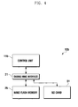
- FIG. 4 illustrates a storage interfacing apparatus according to another exemplary embodiment of the present invention.
- the storage interfacing apparatus 10b of FIG. 4 includes a single control unit 11b, different from the storage interfacing apparatus 10a of FIG. 2.
- the control unit 11b is a control processor performing both communication and multimedia functions.
- the control unit 11b controls and accesses the NAND flash memory 25 supporting the MMC standard and the SD card 31 compatible with the MMC standard through the shared MMC interface 21.
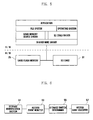
- FIG. 5 illustrates a software architecture for sharing an MMC interface in the apparatus of FIG. 2.
- the software architecture is composed of a shared MMC driver, NAND memory device driver, SD card driver, file system, operating system, and application.
- the second control unit 15 facilitates data access to the NAND flash memory 25 and SD card 31 through the file system, NAND memory device driver, SD card driver, and shared MMC driver in order to execute an application program on top of the operating system.
- the second control unit 15 executes various application programs to perform requested operations, for example, moving image display, audio file playing, photographing with a camera, and electronic dictionary searching.
- the second control unit 15 interprets instructions from the first control unit 11, and makes data access to the NAND flash memory 25 and SD card 31, if necessary.
- the second control unit 15 uses the file system to store and manage data as files and directories.
- FIG. 6 illustrates the second control unit 15 in the apparatus of FIG. 2.
- the second control unit 15 includes a storage identification section 51, an access event monitor 53, a storage switch determiner 55, and an access event executer 57.
- the storage identification section 51 identifies mass storage devices connected to the second control unit 15. In response to occurrence of a reset event, if a mass storage device has no unique identifier, the storage identification section 51 assigns a unique identifier to the mass storage device. If a mass storage device has a unique identifier, the storage identification section 51 reads the unique identifier thereof. For example, for an MMC NAND flash memory 25 that normally has no unique identifier, a unique identifier is assigned thereto by the second control unit 15 acting as a host. For an SD card 31 that has a preset unique identifier, the unique identifier therefrom is read and identified. The second control unit 15 manages unique identifiers of the identified storage devices as relative card addresses (RCA).
- RCA relative card addresses
- the access event monitor 53 monitors access requests to the storage devices identified by the storage identification section 51.
- the access event monitor 53 detects an occurrence of an access request event through monitoring a signal from the first or second input units 41 or 43 or through control of the first control unit 11.
- the storage switch determiner 55 determines whether an access-requested storage device is a current access-selected storage device.
- the storage switch determiner 55 stores necessary information on the access-selected storage device in a memory unit (not shown) composed of, for example, random access memories (RAM).
- RAM random access memories
- the access event executer 57 immediately makes access to the access-selected storage device. If the access-requested storage device is not the access-selected storage device, the access event executer 57 performs an access initialization operation by canceling access-selection of the access-selected storage device and making an access-selection of the access-requested storage device. As storage devices share the control bus line, an access-selection cancel command issued by the second control unit 15 causes all the storage devices to be access-deselected.
- the second control unit 15 After access-deselection, the second control unit 15 sends an access-selection command to the access-requested storage device, and the newly access-selected storage device performs a data transfer operation associated with the access request event. Thereafter, a storage device not access-selected does not respond to an access request event.
- the storage interfacing apparatus 10 enables data access to different kinds of storage devices through a shared MMC interface 21. If the access-requested storage device is the access-selected storage device, the second control unit 15 makes immediate access to the access-selected storage device without access initialization.
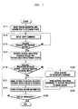
- FIG. 7 is a flow chart illustrating a storage interfacing method according to another exemplary embodiment of the present invention. Referring to FIGS. 3 and 7, the storage interfacing method is described as follows.
- the second control unit 15 In response to an occurrence of a reset event, the second control unit 15 detects available storage devices 25 and 31, recognizes unique identifiers of the detected storage devices 25 and 31, and assigns RCAs thereto (S111). An occurrence of a reset event causes the individual storage devices 25 and 31 to enter into an idle state. The reset event may correspond to a transition of the mobile terminal 100 from a power-off state to a power-on state, or to an access initialization command issued by the second control unit 15. The second control unit 15 sends the content of a storage status register through the control bus line 18, thereby forcing the storage devices 25 and 31 to enter into an inactive state. The second control unit 15 then sends an identifier request command through the control bus line 18.
- the SD card 31 sends a preset unique identifier to the second control unit 15 in reply to the identifier request command.
- the second control unit 15 detects the presence of the SD card 31, reads the unique identifier of the SD card 31, and assigns an RCA of, for example, 2 corresponding to the read unique identifier.
- the second control unit 15 assigns an RCA of, for example, 1 as a unique identifier to the NAND flash memory 25, and sends the assigned RCA to the NAND flash memory 25 through the control bus line 18. Thereby the NAND flash memory 25 and SD card 31 enter into a stand-by state, in which data access is possible.
- the second control unit 15 makes access to the NAND flash memory 25 and SD card 31 using the assigned RCAs.
- the first or second control unit 11 or 15 checks whether an access request event occurs to the NAND flash memory 25 or SD card 31 (S115).
- the first control unit 11 may forward a detected access request event to the second control unit 15.
- the second control unit 15 identifies the access-selected storage device and an access-requested storage device (S 117). That is, the second control unit 15 identifies which of the NAND flash memory 25 and SD card 31 is access-requested.
- the access-selected storage device is identified using storage access information stored in the memory unit (not shown).
- the second control unit 15 determines whether the access-requested storage device is the access-selected storage device (S 119). If the access-requested storage device is the access-selected storage device, the second control unit 15 makes immediate access to the access-selected storage device without access-deselection and access-selection (S121).
- the second control unit 15 issues an access initialization command through the control bus line 18 (S123).
- the access initialization command forces all the storage devices to enter into an inactive state.
- the second control unit 15 then sends an access-selection command through the control bus line 18 to the access-requested storage device (S125).
- the access-requested storage device becomes a new access-selected storage device and enters into a stand-by state.
- the access-selected storage device enters into a data transfer state, and performs a requested data transfer operation (S121).
- the storage devices in the inactive state do not respond to an access request event from the second control unit 15.
- the second control unit 15 stores storage access information regarding the access-selected storage device in the memory unit (S127). Steps S113 to S 127 are repeated until an end-of-operation event such as power-off is determined to have occurred (S129).
- the present invention provides a storage interfacing method and apparatus that enables different types of mass storage devices to share an MMC interface. Thereby the number of pins and size of a control unit are reduced.
- an access-requested storage device is an access-selected storage device, data access to the access-selected storage device is immediately performed without access initialization, thereby enabling fast data transfer.
Landscapes
- Engineering & Computer Science (AREA)
- Theoretical Computer Science (AREA)
- Human Computer Interaction (AREA)
- Physics & Mathematics (AREA)
- General Engineering & Computer Science (AREA)
- General Physics & Mathematics (AREA)
- Computer Networks & Wireless Communication (AREA)
- Signal Processing (AREA)
- Information Retrieval, Db Structures And Fs Structures Therefor (AREA)
- Techniques For Improving Reliability Of Storages (AREA)
- Telephone Function (AREA)
Applications Claiming Priority (1)
| Application Number | Priority Date | Filing Date | Title |
|---|---|---|---|
| KR1020060104672A KR100803005B1 (ko) | 2006-10-26 | 2006-10-26 | 메모리 인터페이싱 방법과 장치 |
Publications (3)
| Publication Number | Publication Date |
|---|---|
| EP1916606A2 true EP1916606A2 (fr) | 2008-04-30 |
| EP1916606A3 EP1916606A3 (fr) | 2008-12-17 |
| EP1916606B1 EP1916606B1 (fr) | 2012-09-19 |
Family
ID=38951465
Family Applications (1)
| Application Number | Title | Priority Date | Filing Date |
|---|---|---|---|
| EP07016089A Not-in-force EP1916606B1 (fr) | 2006-10-26 | 2007-08-16 | Procédé et appareil d'interface de stockage |
Country Status (4)
| Country | Link |
|---|---|
| US (1) | US8010752B2 (fr) |
| EP (1) | EP1916606B1 (fr) |
| KR (1) | KR100803005B1 (fr) |
| CN (1) | CN101169706B (fr) |
Cited By (1)
| Publication number | Priority date | Publication date | Assignee | Title |
|---|---|---|---|---|
| CN102012948A (zh) * | 2010-04-12 | 2011-04-13 | 中国科学院西安光学精密机械研究所 | 基于usb的数据实时采集和存储系统及方法 |
Families Citing this family (6)
| Publication number | Priority date | Publication date | Assignee | Title |
|---|---|---|---|---|
| US8307151B1 (en) | 2009-11-30 | 2012-11-06 | Micron Technology, Inc. | Multi-partitioning feature on e-MMC |
| CN103164362A (zh) * | 2011-12-13 | 2013-06-19 | 联想(北京)有限公司 | 电子设备和存储器控制方法 |
| US9582453B2 (en) * | 2013-08-15 | 2017-02-28 | Western Digital Technologies, Inc. | I/O card architecture based on a common controller |
| US9548867B2 (en) * | 2013-11-26 | 2017-01-17 | Rockwell Automation Technologies, Inc. | Method and apparatus for secure distribution of embedded firmware |
| KR102664665B1 (ko) * | 2016-08-22 | 2024-05-16 | 에스케이하이닉스 주식회사 | 메모리 시스템 |
| JP2023136000A (ja) * | 2022-03-16 | 2023-09-29 | キオクシア株式会社 | メモリシステム |
Family Cites Families (19)
| Publication number | Priority date | Publication date | Assignee | Title |
|---|---|---|---|---|
| US5887145A (en) * | 1993-09-01 | 1999-03-23 | Sandisk Corporation | Removable mother/daughter peripheral card |
| US5717638A (en) * | 1996-11-18 | 1998-02-10 | Samsung Electronics Co., Ltd. | Multi-port memory cells and memory with parallel data initialization |
| US6212598B1 (en) * | 1998-11-30 | 2001-04-03 | Micron Technology, Inc. | Controlling a paging policy based on a requestor characteristic |
| US20080071973A1 (en) * | 2000-01-06 | 2008-03-20 | Chow David Q | Electronic data flash card with various flash memory cells |
| KR200176518Y1 (ko) | 1999-10-26 | 2000-04-15 | 포항종합제철주식회사 | 가역 벨트 콘베어용 벨트 사행 조정장치 |
| KR100383774B1 (ko) * | 2000-01-26 | 2003-05-12 | 삼성전자주식회사 | 공통 인터페이스 방식의 메모리 장치들을 구비한 시스템 |
| KR20020016430A (ko) | 2000-08-25 | 2002-03-04 | 윤종용 | 멀티미디어 모듈러 카드와 모듈러 카드 운영장치 및통합형 멀티미디어 시스템 |
| US6763437B1 (en) * | 2000-09-07 | 2004-07-13 | Maxtor Corporation | Control system, storage device and method for controlling access to a shared memory using a bus control or handshaking protocol |
| US6526483B1 (en) | 2000-09-20 | 2003-02-25 | Broadcom Corporation | Page open hint in transactions |
| KR100429872B1 (ko) * | 2001-06-27 | 2004-05-04 | 삼성전자주식회사 | 반도체 메모리 장치의 이용 효율을 높이는 메모리 시스템및 상기 반도체 메모리 장치의 리프레쉬 방법 |
| US7162549B2 (en) * | 2001-10-29 | 2007-01-09 | Onspec Electronics, Inc. | Multimode controller for intelligent and “dumb” flash cards |
| US6799257B2 (en) * | 2002-02-21 | 2004-09-28 | Intel Corporation | Method and apparatus to control memory accesses |
| TWI222028B (en) | 2002-06-07 | 2004-10-11 | Carry Computer Eng Co Ltd | Switching method and judgment method of common connector and terminals of memory card |
| US7200743B1 (en) * | 2002-09-30 | 2007-04-03 | Mindspeed Technologies, Inc. | Simultaneous initialization of a plurality of memory elements from among a plurality of initialization values |
| KR100618814B1 (ko) * | 2003-07-04 | 2006-08-31 | 삼성전자주식회사 | 다중 호스트 인터페이스를 지원하는 스마트 카드 겸용이동형 저장 장치 및 이에 대한 인터페이스 방법 |
| KR100703357B1 (ko) * | 2003-08-16 | 2007-04-03 | 삼성전자주식회사 | 보조제어부를 구비하는 휴대용 단말기의 캐시메모리구현장치 및 방법 |
| US7165161B2 (en) | 2003-12-09 | 2007-01-16 | Intel Corporation | Methods and apparatus for balancing memory access latency and bandwidth |
| US7822146B2 (en) * | 2006-12-01 | 2010-10-26 | Texas Instruments Incorporated | System and method for digitally correcting a non-linear element |
| US7729446B2 (en) * | 2006-12-01 | 2010-06-01 | Texas Instruments Incorporated | System and method for digitally correcting a non-linear element using a multiply partitioned architecture for predistortion |
-
2006
- 2006-10-26 KR KR1020060104672A patent/KR100803005B1/ko not_active Expired - Fee Related
-
2007
- 2007-06-22 US US11/821,273 patent/US8010752B2/en not_active Expired - Fee Related
- 2007-08-16 EP EP07016089A patent/EP1916606B1/fr not_active Not-in-force
- 2007-08-24 CN CN2007101477145A patent/CN101169706B/zh not_active Expired - Fee Related
Cited By (2)
| Publication number | Priority date | Publication date | Assignee | Title |
|---|---|---|---|---|
| CN102012948A (zh) * | 2010-04-12 | 2011-04-13 | 中国科学院西安光学精密机械研究所 | 基于usb的数据实时采集和存储系统及方法 |
| CN102012948B (zh) * | 2010-04-12 | 2012-08-29 | 中国科学院西安光学精密机械研究所 | 基于usb的数据实时采集和存储系统及方法 |
Also Published As
| Publication number | Publication date |
|---|---|
| KR100803005B1 (ko) | 2008-02-14 |
| CN101169706B (zh) | 2012-05-09 |
| CN101169706A (zh) | 2008-04-30 |
| US8010752B2 (en) | 2011-08-30 |
| EP1916606B1 (fr) | 2012-09-19 |
| EP1916606A3 (fr) | 2008-12-17 |
| US20080104304A1 (en) | 2008-05-01 |
Similar Documents
| Publication | Publication Date | Title |
|---|---|---|
| EP1916606B1 (fr) | Procédé et appareil d'interface de stockage | |
| US6928543B2 (en) | System for real-time adaptation to changes in display configuration | |
| US7007127B2 (en) | Method and related apparatus for controlling transmission interface between an external device and a computer system | |
| CA2082118C (fr) | Ordinateur et dispositif et methode de reconfiguration connexes | |
| US8356118B2 (en) | Storage device and storage device access control method | |
| JP3403284B2 (ja) | 情報処理システム及びその制御方法 | |
| JP4166326B2 (ja) | 集積化グラフィックスコントローラを備えた1チップのチップセット | |
| JP3090671U (ja) | ダブルインターフェースcfフラッシュメモリカード | |
| US8688896B2 (en) | High speed writing mode in memory controller, nonvolatile storage device, accessing device, nonvolatile storage system, and method and program for writing data | |
| US7975101B2 (en) | Storage medium storing drive configuration setting program | |
| US20130038888A1 (en) | Printer With USB Interface and Driver Installing Method and System Thereof | |
| KR20040011103A (ko) | 카드 삽입 인식에 의한 데이터 전송 상태 자동 설정 장치및 방법 | |
| JPH11126182A (ja) | コンピュータバス間通信装置及びその方法 | |
| US6065083A (en) | Increasing I/O performance through storage of packetized operational information in local memory | |
| CN110413554B (zh) | 热插拔系统及热插拔方法 | |
| US20060190637A1 (en) | Control apparatus, information processing apparatus, and data transferring method | |
| CN101329661B (zh) | 一种实现hid/scsi设备pc/sc接口的系统和方法 | |
| CN114238194A (zh) | Usb组合设备和枚举方法 | |
| CN116185509A (zh) | 时钟展频功能设置方法、装置、电子设备及存储介质 | |
| US20080077712A1 (en) | Peripheral device, peripheral-device recognizing method, and computer product | |
| JP4793798B2 (ja) | マイクロコンピュータ | |
| CN112559402A (zh) | 一种基于fpga的pci从接口控制电路及fpga | |
| US5832277A (en) | System for arbitrating demand on memory during configuration of a computer add-on card | |
| KR100633120B1 (ko) | 저장 매체의 데이터 대역폭 향상 방법 및 이를 위한 장치 | |
| JP2719419B2 (ja) | Icカード |
Legal Events
| Date | Code | Title | Description |
|---|---|---|---|
| PUAI | Public reference made under article 153(3) epc to a published international application that has entered the european phase |
Free format text: ORIGINAL CODE: 0009012 |
|
| 17P | Request for examination filed |
Effective date: 20070816 |
|
| AK | Designated contracting states |
Kind code of ref document: A2 Designated state(s): AT BE BG CH CY CZ DE DK EE ES FI FR GB GR HU IE IS IT LI LT LU LV MC MT NL PL PT RO SE SI SK TR |
|
| AX | Request for extension of the european patent |
Extension state: AL BA HR MK RS |
|
| PUAL | Search report despatched |
Free format text: ORIGINAL CODE: 0009013 |
|
| AK | Designated contracting states |
Kind code of ref document: A3 Designated state(s): AT BE BG CH CY CZ DE DK EE ES FI FR GB GR HU IE IS IT LI LT LU LV MC MT NL PL PT RO SE SI SK TR |
|
| AX | Request for extension of the european patent |
Extension state: AL BA HR MK RS |
|
| AKX | Designation fees paid |
Designated state(s): DE FR GB |
|
| 17Q | First examination report despatched |
Effective date: 20090731 |
|
| GRAP | Despatch of communication of intention to grant a patent |
Free format text: ORIGINAL CODE: EPIDOSNIGR1 |
|
| GRAJ | Information related to disapproval of communication of intention to grant by the applicant or resumption of examination proceedings by the epo deleted |
Free format text: ORIGINAL CODE: EPIDOSDIGR1 |
|
| GRAP | Despatch of communication of intention to grant a patent |
Free format text: ORIGINAL CODE: EPIDOSNIGR1 |
|
| GRAS | Grant fee paid |
Free format text: ORIGINAL CODE: EPIDOSNIGR3 |
|
| GRAA | (expected) grant |
Free format text: ORIGINAL CODE: 0009210 |
|
| AK | Designated contracting states |
Kind code of ref document: B1 Designated state(s): DE FR GB |
|
| RAP1 | Party data changed (applicant data changed or rights of an application transferred) |
Owner name: SAMSUNG ELECTRONICS CO., LTD. |
|
| REG | Reference to a national code |
Ref country code: GB Ref legal event code: FG4D |
|
| REG | Reference to a national code |
Ref country code: DE Ref legal event code: R096 Ref document number: 602007025526 Country of ref document: DE Effective date: 20121108 |
|
| PLBE | No opposition filed within time limit |
Free format text: ORIGINAL CODE: 0009261 |
|
| STAA | Information on the status of an ep patent application or granted ep patent |
Free format text: STATUS: NO OPPOSITION FILED WITHIN TIME LIMIT |
|
| 26N | No opposition filed |
Effective date: 20130620 |
|
| REG | Reference to a national code |
Ref country code: DE Ref legal event code: R097 Ref document number: 602007025526 Country of ref document: DE Effective date: 20130620 |
|
| REG | Reference to a national code |
Ref country code: FR Ref legal event code: PLFP Year of fee payment: 9 |
|
| PGFP | Annual fee paid to national office [announced via postgrant information from national office to epo] |
Ref country code: GB Payment date: 20150721 Year of fee payment: 9 Ref country code: DE Payment date: 20150722 Year of fee payment: 9 |
|
| PGFP | Annual fee paid to national office [announced via postgrant information from national office to epo] |
Ref country code: FR Payment date: 20150625 Year of fee payment: 9 |
|
| REG | Reference to a national code |
Ref country code: DE Ref legal event code: R119 Ref document number: 602007025526 Country of ref document: DE |
|
| GBPC | Gb: european patent ceased through non-payment of renewal fee |
Effective date: 20160816 |
|
| REG | Reference to a national code |
Ref country code: FR Ref legal event code: ST Effective date: 20170428 |
|
| PG25 | Lapsed in a contracting state [announced via postgrant information from national office to epo] |
Ref country code: GB Free format text: LAPSE BECAUSE OF NON-PAYMENT OF DUE FEES Effective date: 20160816 Ref country code: DE Free format text: LAPSE BECAUSE OF NON-PAYMENT OF DUE FEES Effective date: 20170301 Ref country code: FR Free format text: LAPSE BECAUSE OF NON-PAYMENT OF DUE FEES Effective date: 20160831 |