EP1920461B1 - Procédé de fabrication d'interconnexions verticales dans des plaquettes semi-conductrices - Google Patents
Procédé de fabrication d'interconnexions verticales dans des plaquettes semi-conductrices Download PDFInfo
- Publication number
- EP1920461B1 EP1920461B1 EP06792559.4A EP06792559A EP1920461B1 EP 1920461 B1 EP1920461 B1 EP 1920461B1 EP 06792559 A EP06792559 A EP 06792559A EP 1920461 B1 EP1920461 B1 EP 1920461B1
- Authority
- EP
- European Patent Office
- Prior art keywords
- wafer
- laser
- rear side
- etching
- contacts
- Prior art date
- Legal status (The legal status is an assumption and is not a legal conclusion. Google has not performed a legal analysis and makes no representation as to the accuracy of the status listed.)
- Not-in-force
Links
Images


Classifications
-
- H—ELECTRICITY
- H10—SEMICONDUCTOR DEVICES; ELECTRIC SOLID-STATE DEVICES NOT OTHERWISE PROVIDED FOR
- H10W—GENERIC PACKAGES, INTERCONNECTIONS, CONNECTORS OR OTHER CONSTRUCTIONAL DETAILS OF DEVICES COVERED BY CLASS H10
- H10W20/00—Interconnections in chips, wafers or substrates
- H10W20/01—Manufacture or treatment
- H10W20/021—Manufacture or treatment of interconnections within wafers or substrates
- H10W20/023—Manufacture or treatment of interconnections within wafers or substrates the interconnections being through-semiconductor vias
-
- H—ELECTRICITY
- H10—SEMICONDUCTOR DEVICES; ELECTRIC SOLID-STATE DEVICES NOT OTHERWISE PROVIDED FOR
- H10P—GENERIC PROCESSES OR APPARATUS FOR THE MANUFACTURE OR TREATMENT OF DEVICES COVERED BY CLASS H10
- H10P50/00—Etching of wafers, substrates or parts of devices
- H10P50/20—Dry etching; Plasma etching; Reactive-ion etching
- H10P50/24—Dry etching; Plasma etching; Reactive-ion etching of semiconductor materials
- H10P50/242—Dry etching; Plasma etching; Reactive-ion etching of semiconductor materials of Group IV materials
-
- H—ELECTRICITY
- H10—SEMICONDUCTOR DEVICES; ELECTRIC SOLID-STATE DEVICES NOT OTHERWISE PROVIDED FOR
- H10P—GENERIC PROCESSES OR APPARATUS FOR THE MANUFACTURE OR TREATMENT OF DEVICES COVERED BY CLASS H10
- H10P50/00—Etching of wafers, substrates or parts of devices
- H10P50/20—Dry etching; Plasma etching; Reactive-ion etching
- H10P50/24—Dry etching; Plasma etching; Reactive-ion etching of semiconductor materials
- H10P50/246—Dry etching; Plasma etching; Reactive-ion etching of semiconductor materials of Group III-V materials
-
- H—ELECTRICITY
- H10—SEMICONDUCTOR DEVICES; ELECTRIC SOLID-STATE DEVICES NOT OTHERWISE PROVIDED FOR
- H10P—GENERIC PROCESSES OR APPARATUS FOR THE MANUFACTURE OR TREATMENT OF DEVICES COVERED BY CLASS H10
- H10P70/00—Cleaning of wafers, substrates or parts of devices
- H10P70/20—Cleaning during device manufacture
-
- H—ELECTRICITY
- H10—SEMICONDUCTOR DEVICES; ELECTRIC SOLID-STATE DEVICES NOT OTHERWISE PROVIDED FOR
- H10W—GENERIC PACKAGES, INTERCONNECTIONS, CONNECTORS OR OTHER CONSTRUCTIONAL DETAILS OF DEVICES COVERED BY CLASS H10
- H10W20/00—Interconnections in chips, wafers or substrates
- H10W20/01—Manufacture or treatment
- H10W20/021—Manufacture or treatment of interconnections within wafers or substrates
- H10W20/023—Manufacture or treatment of interconnections within wafers or substrates the interconnections being through-semiconductor vias
- H10W20/0234—Manufacture or treatment of interconnections within wafers or substrates the interconnections being through-semiconductor vias comprising etching via holes that stop on pads or on electrodes
-
- H—ELECTRICITY
- H10—SEMICONDUCTOR DEVICES; ELECTRIC SOLID-STATE DEVICES NOT OTHERWISE PROVIDED FOR
- H10W—GENERIC PACKAGES, INTERCONNECTIONS, CONNECTORS OR OTHER CONSTRUCTIONAL DETAILS OF DEVICES COVERED BY CLASS H10
- H10W20/00—Interconnections in chips, wafers or substrates
- H10W20/01—Manufacture or treatment
- H10W20/021—Manufacture or treatment of interconnections within wafers or substrates
- H10W20/023—Manufacture or treatment of interconnections within wafers or substrates the interconnections being through-semiconductor vias
- H10W20/0242—Manufacture or treatment of interconnections within wafers or substrates the interconnections being through-semiconductor vias comprising etching via holes from the back sides of the chips, wafers or substrates
Definitions
- the invention relates to a method for producing vertical plated-through holes (micro vias, blind hole vias or via connections) in semiconductor wafers for producing semiconductor components, that is to say from contacts on the wafer front side through the semiconductor wafer. Wafer through to the wafer back.
- vertical plated-through holes micro vias, blind hole vias or via connections
- GaN gallium nitride
- SiC wafers silicon carbide
- SiC is characterized by a very good thermal conductivity as well as an extremely high chemical stability and high hardness.
- Virtually only dry-chemical etching processes such as reactive ion etching in specially optimized high-performance plasma etching reactors have been considered for structuring.
- typical plasma etching rates of SiC are very small at 1 ⁇ m / min.
- the use of the plasma etching technique also requires the production and lithographic structuring of a resistant etching mask.
- vias can be produced in printed circuit boards by the use of lasers.
- the laser drills holes in the copper and dielectric layers and then metallizes them to make electrical connections between specific layers.
- the different laser technologies are based on the use of CO 2 lasers, frequency-doubled (green) YAG lasers, excimer lasers and UV: YAG lasers.
- US 2001/035580 A1 deals with the through-plating of GaN semiconductor devices on sapphire or SiC substrates and can serve to illustrate the technical background of the invention.
- the invention has for its object to provide an effective method for the production of micro vias in semiconductor wafers, in particular from materials of high hardness and chemical stability such as silicon carbide, sapphire or the like.
- a protective coating can be applied to the wafer front, which is removed after the process (peeling off).
- the wafer back can be coated with indium tin oxide (ITO) before the laser drilling of the blind holes, which can be easily removed after plasma etching.
- ITO indium tin oxide
- the cleaning of the wafer to remove the debris in the case of SiC substrate material is expediently carried out with buffered hydrofluoric acid.
- a material-selective etching method for the semiconductor substrate is preferably the ICP etching method (inductivelycoupled plasma), for the layer stack, the RIE method (reactive ion etching).
- the laser is a UV laser, preferably a frequency-tripled Nd: YAG laser with a wavelength of 355 nm.
- the application of the plating base in the micro-vias can be done with several methods.
- An oblique vapor deposition, a chemical bath deposition (de-energized) or a sputtering are also possible.
- an anti-wetting layer can be applied to the gold layer locally at the micro-vias.
- the dewetting layer is suitably used titanium, which can be sputtered.
- the order of the anti-wetting layer is expediently carried out with the aid of a shadow mask.
- the method has the advantage that micro-vias can be produced in hard and chemically inert substrate materials with significantly reduced time and with high precision.
- the method of micromaterial processing by means of UV laser radiation is used in combination with plasma etching and used for the direct structuring in the component manufacturing.
- plasma etching removes material selectively from the residual material to the front contacts.
- Etch mask does not need to be lithographically generated, but the laser drilled holes serve as an etching mask. If the machining side is properly protected, the material thickness is maintained. A protective layer, which is pierced by the laser, in this case prevents the flat material removal during plasma etching. In the absence of the protective layer, there is a large-scale ⁇ tzabtrag. The concomitant decrease in material thickness can be estimated over the known etching rates.
- a wafer having a transistor structure is shown in cross-section.
- the wafer consists of a SiC substrate 1 of about 250 to 400 microns thick thickness, on which an AlGaN / GaN layer stack 2 of about 2 to 3 microns thick is epitaxially grown.
- the terminal contacts of a transistor namely a drain contact 3, a gate contact 4 and a source contact 5.
- the potential of the source contact 5 must on the back (ground electrode 6) of the wafer, which takes place with the aid of a micro-vias 7 whose perforated walls 8 are metallized, so that the source contact 5 on the front side is electrically connected to the ground electrode 6 on the backside of the wafer.
- the process control of the process according to the invention and the results obtained are described below.
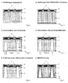
- the process sequence is in the Fig. 2 to 8 shown schematically.
- the finished processed GaN transistors or MMICs are provided in the wafer composite with the micro-vias 7.
- a protective varnish 9 is applied to the wafer front side in order to protect the wafers during the following process steps ( Fig. 2 ).
- the back surface is covered over a large area with a 2 ⁇ m thick protective layer 10 made of indium tin oxide (ITO) ( Fig. 3 ).
- ITO indium tin oxide
- This protective layer 10 then serves as protection of the SiC surface during etching and is removed during subsequent drilling by a laser at the via-inlet openings.
- Now blind holes 11 are drilled from the back side of the wafer with the laser ( FIG. 4 ).
- the laser beam which has a diameter of approximately 15 ⁇ m, is expediently moved on the wafer.
- the beam movement and laser parameters can be set in such a way that a surface profile that is as level as possible is formed close to the SiC / GaN interface.
- Loose particles that are deposited on the sample during the drilling process are then removed in a wet-chemical cleaning step. Etching in buffered hydrofluoric acid with ultrasound is suitable for this purpose.
- the blind holes 11 predrilled with the laser are then dry-chemically etched through plasma etching to the front-side contacts ( Fig. 5 ).
- the remaining SiC is removed by means of ICP etching in fluorine-containing gas mixtures (for example sulfur hexafluoride-oxygen-helium-SF 6 -O 2 -He).
- fluorine-containing gas mixtures for example sulfur hexafluoride-oxygen-helium-SF 6 -O 2 -He.
- the removal of the 2-3 ⁇ m thin epitaxial layer of AlGaN / GaN takes place plasma-chemically with an RIE process, for example with boron trichloride-chlorine (BCl 3 -Cl 2 ).
- the selectivity of the dry chemical etching process of GaN vs. Platinum is> 10: 1.
- the metal layer of the front side contact with a total thickness of about 5 microns is thus removed only very slowly, ie the etching process stops practically at Metal layer. An undercut does not occur.
- a lying below the platinum contacts titanium layer of some 10 nm is removed with.
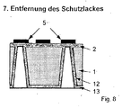
- the possibly applied layer 10 can be removed again, which is expediently carried out with iron (III) chloride ( Fig. 6 ).
- a thin metal layer 12 is subsequently vapor-deposited on the wafer backside.
- a closed occupancy of the hole walls is achieved by Schrägbedampfung according to this embodiment.
- Other metallization processes such as sputtering or electroless chemical deposition are also possible.
- the plating base obtained by the metal layer 12 is then galvanically reinforced by a gold layer 5, typically 5 ⁇ m thick ( Fig. 7 ). In this way, an electrical connection is made from the one wafer side to the other side with a closed gold layer 13.
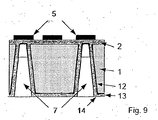
- an anti-wetting layer 14 made of titanium can also be applied to the via entry openings on the rear side, namely a titanium layer 100 nm thick, which is sputtered onto the existing gold layer 13.
- the anti-wetting layer 14 is applied to the wafer in a structured manner with the aid of a shadow mask.
- the shadow mask consists of a 0.1 mm thick metal foil in which holes are drilled with the laser.
- the layout of the openings in the metal foil corresponds to the arrangement of the micro-vias 7 on the wafer.
- the diameters of the openings in the shadow mask are slightly larger than the entry diameter of the micro-vias 7 on the back of the wafer, so that an approximately 40 ⁇ m wide titanium ring is formed around the via entry openings.
- the lacquering of the protective lacquer 9 can also take place only after the deposition of the anti-wetting layer 14 (titanium dewetting layer).
- FIG. 9 A schematic representation of the finished micro-vias 7 in cross-section shows Fig. 9 .
- the ITO masking of the surface can also be dispensed with if a controlled decrease in the material thickness during the etching process is acceptable, that is to say the steps according to FIGS 3 and 6 omitted.
- the process flow for this case is based on the 10 to 14 demonstrated.
- the process steps then correspond to process steps 1, 3, 4, 6 and 7 of the first example (corresponding to FIGS FIGS. 2, 4, 5, 7 and 8th ).
- the total thickness of the wafer decreases due to the large-area removal of the SiC.
- the wafer With an etching time of about 2 h, the wafer is thinned from 390 ⁇ m to 250-300 ⁇ m.
- an edge length of 35-70 microns is obtained, the corners are widened hexagonal.
- the hole shape is conical with a clear widening of the cross section at the entrance, whereby the subsequent occupancy of the hole wall is facilitated with metal.
- a frequency-tripled Nd: YAG laser is well suited for processing very hard and chemically inert SiC.
- This laser delivers nanosecond pulses of high energy in the ultraviolet spectral range at a wavelength of 355 nm with pulse rates of up to 100 kHz.
- the laser beam is moved micrometer-accurate by combining the CNC-controlled movement of the sample stage and the beam deflection with a galvo scanner.
- the laser beam can be positioned with an accuracy of ⁇ 1 ⁇ m with respect to existing structures on the workpiece. This precision is also achieved when the laser patterning is done on the back side and the alignment marks are on the (lower) front side.
- the edge length was about 75 microns at the laser entrance, at the hole bottom, it was about 15 microns, about 40 microns SiC remained below the bottom of the hole.
- Resistance measurements on a SiC sample prove that a low-resistance connection can be established between both sides.
- samples were first metallized on one side over the entire surface with a 5 ⁇ m thick gold layer before the via processing. From the other side, a matrix of vias was generated as described above. The hole spacing was 500 ⁇ m. Before measuring the resistance through a single hole, the individual holes had to be electrically separated from each other. For this purpose, the gold layer was cut through (scratched) to 500x500 microns 2 large fields, each with a via to get. It could be shown that the contacting through the SiC sample was realized with good reproducibility and very homogeneous.
- the resistance values are 25-31 m ⁇ .
- the mean value over the 206 micro-vias is 27 ⁇ 2 m ⁇ .
- the realized hollow rivets have an aspect ratio of 3-4.
- the prerequisite for the application of laser micromachining in the processing of semiconductor wafers is a high positioning accuracy of the beam center point of ⁇ 1 ⁇ m and better. This accuracy relates to the beam positioning relative to existing device structures and must be achieved in both the front and back side processing.
- the invention enables vias through the very hard and chemically resistant silicon carbide. An aspect ratio of 3-4 was demonstrated for this purpose.
Landscapes
- Internal Circuitry In Semiconductor Integrated Circuit Devices (AREA)
- Drying Of Semiconductors (AREA)
- Laser Beam Processing (AREA)
- Junction Field-Effect Transistors (AREA)
- Weting (AREA)
Claims (15)
- Procédé de production de métallisation de trous verticaux pour la réalisation de composants semi-conducteurs, c'est-à-dire de contacts sur la face avant de plaquette à travers la plaquette semi-conductrice vers la face arrière de plaquette, la plaquette présentant un substrat (1) en matériau de substrat et une pile de couches (2) électriquement active mise en place sur le substrat (1) avec une couche épitaxiale GaN,
comprenant les étapes suivantes :- perçage au laser de trous borgnes (11) aux points de liaison de contact à partir de la face arrière de plaquette (6) dans le substrat semi-conducteur- nettoyage de la plaquette- gravure au plasma par sélection de matière du substrat semi-conducteur jusqu'à la pile de couches active de la plaquette- gravure au plasma par sélection de matière de la pile de couches (2) active de la plaquette jusqu'à ce que l'on atteigne les contacts à relier à la face arrière de plaquette (6)- mise en place d'une base plaquée (12) sur la face arrière de plaquette (6) et dans les trous borgnes (11) produits dans une étape précédente- application d'or (13) par voie galvanique sur la face arrière de plaquette (6) métallisée et sur les trous borgnes (11) munis d'une base plaquée (12) dans une étape précédente. - Procédé selon la revendication 1, caractérisé en ce que,
avant le perçage au laser des trous borgnes (11), un vernis de protection (9) est appliqué sur la face avant de plaquette et est ensuite enlevé après l'application d'or (13). - Procédé selon la revendication 1 ou 2, caractérisé en ce que,
avant le perçage au laser des trous borgnes (11), la face arrière de plaquette (6) est revêtue d'oxyde d'indium-étain (ITO) qui est enlevé ensuite après l'application d'or (13). - Procédé selon l'une des revendications 1 à 3, caractérisé en ce que le nettoyage s'effectue par voie chimique humide au moyen d'acide fluorhydrique tamponné.
- Procédé selon l'une des revendications précédentes, caractérisé en ce que, dans la zone des ouvertures d'entrée des trous débouchants sur la face arrière de plaquette (6), une couche anti-mouillage (14) est appliquée sur l'application d'or (13) galvanique.
- Procédé selon la revendication 5, caractérisé en ce que du titane est utilisé pour la couche anti-mouillage (14).
- Procédé selon la revendication 5 ou 6, caractérisé en ce que la couche anti-mouillage (14) est déposée par pulvérisation.
- Procédé selon l'une des revendications 5 à 7, caractérisé en ce que l'application de la couche anti-mouillage (14) s'effectue à l'aide d'un masque perforé.
- Procédé selon l'une des revendications précédentes, caractérisé en ce qu'un laser UV est utilisé pour le perçage au laser.
- Procédé selon l'une des revendications précédentes, caractérisé en ce que l'application de la base plaquée (12) s'effectue par dépôt par évaporation oblique.
- Procédé selon l'une des revendications 1 à 9, caractérisé en ce que l'application de la base plaquée (12) s'effectue par pulvérisation.
- Procédé selon l'une des revendications 1 à 9, caractérisé en ce que l'application de la base plaquée (12) s'effectue par dépôt en bain chimique.
- Procédé selon l'une des revendications précédentes, caractérisé en ce que, pour le perçage au laser, il est utilisé un laser dont le faisceau est plus petit que la surface de section transversale du trou borgne (11) à produire, le faisceau étant déplacé au-dessus de la zone du trou borgne (11).
- Procédé selon l'une des revendications précédentes, caractérisé en ce que la gravure au plasma du substrat semi-conducteur s'effectue par gravure ICP.
- Procédé selon l'une des revendications précédentes, caractérisé en ce que la gravure au plasma de la pile de couche (2) active s'effectue par gravure RIE.
Applications Claiming Priority (2)
| Application Number | Priority Date | Filing Date | Title |
|---|---|---|---|
| DE102005042074A DE102005042074A1 (de) | 2005-08-31 | 2005-08-31 | Verfahren zur Erzeugung von Durchkontaktierungen in Halbleiterwafern |
| PCT/EP2006/064599 WO2007025812A1 (fr) | 2005-08-31 | 2006-07-24 | Procede de realisation de metallisation des trous de plaquettes semi-conductrices |
Publications (2)
| Publication Number | Publication Date |
|---|---|
| EP1920461A1 EP1920461A1 (fr) | 2008-05-14 |
| EP1920461B1 true EP1920461B1 (fr) | 2016-11-16 |
Family
ID=37076379
Family Applications (1)
| Application Number | Title | Priority Date | Filing Date |
|---|---|---|---|
| EP06792559.4A Not-in-force EP1920461B1 (fr) | 2005-08-31 | 2006-07-24 | Procédé de fabrication d'interconnexions verticales dans des plaquettes semi-conductrices |
Country Status (5)
| Country | Link |
|---|---|
| US (1) | US8455355B2 (fr) |
| EP (1) | EP1920461B1 (fr) |
| JP (1) | JP5123185B2 (fr) |
| DE (1) | DE102005042074A1 (fr) |
| WO (1) | WO2007025812A1 (fr) |
Families Citing this family (32)
| Publication number | Priority date | Publication date | Assignee | Title |
|---|---|---|---|---|
| US7091124B2 (en) | 2003-11-13 | 2006-08-15 | Micron Technology, Inc. | Methods for forming vias in microelectronic devices, and methods for packaging microelectronic devices |
| US8084866B2 (en) | 2003-12-10 | 2011-12-27 | Micron Technology, Inc. | Microelectronic devices and methods for filling vias in microelectronic devices |
| US20050247894A1 (en) | 2004-05-05 | 2005-11-10 | Watkins Charles M | Systems and methods for forming apertures in microfeature workpieces |
| US7232754B2 (en) | 2004-06-29 | 2007-06-19 | Micron Technology, Inc. | Microelectronic devices and methods for forming interconnects in microelectronic devices |
| US7425499B2 (en) | 2004-08-24 | 2008-09-16 | Micron Technology, Inc. | Methods for forming interconnects in vias and microelectronic workpieces including such interconnects |
| SG120200A1 (en) | 2004-08-27 | 2006-03-28 | Micron Technology Inc | Slanted vias for electrical circuits on circuit boards and other substrates |
| US7300857B2 (en) | 2004-09-02 | 2007-11-27 | Micron Technology, Inc. | Through-wafer interconnects for photoimager and memory wafers |
| US7271482B2 (en) | 2004-12-30 | 2007-09-18 | Micron Technology, Inc. | Methods for forming interconnects in microelectronic workpieces and microelectronic workpieces formed using such methods |
| US7795134B2 (en) | 2005-06-28 | 2010-09-14 | Micron Technology, Inc. | Conductive interconnect structures and formation methods using supercritical fluids |
| US7262134B2 (en) | 2005-09-01 | 2007-08-28 | Micron Technology, Inc. | Microfeature workpieces and methods for forming interconnects in microfeature workpieces |
| US7863187B2 (en) | 2005-09-01 | 2011-01-04 | Micron Technology, Inc. | Microfeature workpieces and methods for forming interconnects in microfeature workpieces |
| US7749899B2 (en) | 2006-06-01 | 2010-07-06 | Micron Technology, Inc. | Microelectronic workpieces and methods and systems for forming interconnects in microelectronic workpieces |
| US7629249B2 (en) | 2006-08-28 | 2009-12-08 | Micron Technology, Inc. | Microfeature workpieces having conductive interconnect structures formed by chemically reactive processes, and associated systems and methods |
| US7902643B2 (en) | 2006-08-31 | 2011-03-08 | Micron Technology, Inc. | Microfeature workpieces having interconnects and conductive backplanes, and associated systems and methods |
| DE102007019552B4 (de) * | 2007-04-25 | 2009-12-17 | Infineon Technologies Ag | Verfahren zur Herstellung eines Substrats mit Durchführung sowie Substrat und Halbleitermodul mit Durchführung |
| JP5228381B2 (ja) * | 2007-06-25 | 2013-07-03 | 三菱電機株式会社 | 半導体装置の製造方法 |
| SG149710A1 (en) | 2007-07-12 | 2009-02-27 | Micron Technology Inc | Interconnects for packaged semiconductor devices and methods for manufacturing such devices |
| SG150410A1 (en) | 2007-08-31 | 2009-03-30 | Micron Technology Inc | Partitioned through-layer via and associated systems and methods |
| US7884015B2 (en) | 2007-12-06 | 2011-02-08 | Micron Technology, Inc. | Methods for forming interconnects in microelectronic workpieces and microelectronic workpieces formed using such methods |
| CA2708114C (fr) * | 2009-06-18 | 2017-11-14 | Lin-ping SHEN | Matrice buttler et antenne a mise en forme des faisceaux ainsi constituee |
| US20110209432A1 (en) * | 2010-03-01 | 2011-09-01 | Downey Mike A | Metal "slip clip" to hold metal studes in top track of commercial interior framing |
| CN101916754B (zh) * | 2010-06-29 | 2012-08-29 | 香港应用科技研究院有限公司 | 通孔和通孔形成方法以及通孔填充方法 |
| JP5566803B2 (ja) * | 2010-07-21 | 2014-08-06 | 住友電工デバイス・イノベーション株式会社 | 半導体装置の製造方法 |
| KR101219386B1 (ko) * | 2011-02-16 | 2013-01-21 | 한국기계연구원 | 관통형 실리콘 비아의 가공방법 및 그에 의해 제조된 반도체 칩 |
| JP2013058624A (ja) * | 2011-09-08 | 2013-03-28 | Mitsubishi Electric Corp | レーザダイオード素子の製造方法 |
| CN102768950A (zh) * | 2012-07-12 | 2012-11-07 | 江苏扬景光电有限公司 | 一种混合式蚀刻产生氮化物器件衬底的孔洞的方法 |
| KR101988893B1 (ko) * | 2012-12-12 | 2019-09-30 | 한국전자통신연구원 | 반도체 소자 및 이를 제조하는 방법 |
| JP6309211B2 (ja) * | 2013-06-14 | 2018-04-11 | 新電元工業株式会社 | 炭化ケイ素半導体装置 |
| JP2015002299A (ja) * | 2013-06-17 | 2015-01-05 | 株式会社ザイキューブ | 漏斗状の貫通電極およびその製造方法 |
| CN107980171B (zh) * | 2016-12-23 | 2022-06-24 | 苏州能讯高能半导体有限公司 | 半导体芯片、半导体晶圆及半导体晶圆的制造方法 |
| US10269756B2 (en) * | 2017-04-21 | 2019-04-23 | Invensas Bonding Technologies, Inc. | Die processing |
| JP7076576B2 (ja) * | 2018-12-27 | 2022-05-27 | 三菱電機株式会社 | 半導体素子構造 |
Family Cites Families (20)
| Publication number | Priority date | Publication date | Assignee | Title |
|---|---|---|---|---|
| US4473737A (en) * | 1981-09-28 | 1984-09-25 | General Electric Company | Reverse laser drilling |
| US4897708A (en) * | 1986-07-17 | 1990-01-30 | Laser Dynamics, Inc. | Semiconductor wafer array |
| US5371042A (en) * | 1992-06-16 | 1994-12-06 | Applied Materials, Inc. | Method of filling contacts in semiconductor devices |
| JP3724110B2 (ja) * | 1997-04-24 | 2005-12-07 | 三菱電機株式会社 | 半導体装置の製造方法 |
| JP4264992B2 (ja) * | 1997-05-28 | 2009-05-20 | ソニー株式会社 | 半導体装置の製造方法 |
| US6239033B1 (en) | 1998-05-28 | 2001-05-29 | Sony Corporation | Manufacturing method of semiconductor device |
| JP2868008B1 (ja) * | 1997-11-21 | 1999-03-10 | 日本電気株式会社 | 半導体装置及びその製造方法 |
| DE69737262T2 (de) * | 1997-11-26 | 2007-11-08 | Stmicroelectronics S.R.L., Agrate Brianza | Herstellungsverfahren für einen Vorder-Hinterseiten-Durchkontakt in mikro-integrierten Schaltungen |
| JPH11238870A (ja) * | 1998-02-20 | 1999-08-31 | Nec Corp | 半導体装置とその製造方法 |
| US7125786B2 (en) * | 2000-04-11 | 2006-10-24 | Cree, Inc. | Method of forming vias in silicon carbide and resulting devices and circuits |
| US6475889B1 (en) * | 2000-04-11 | 2002-11-05 | Cree, Inc. | Method of forming vias in silicon carbide and resulting devices and circuits |
| US20020086520A1 (en) * | 2001-01-02 | 2002-07-04 | Advanced Semiconductor Engineering Inc. | Semiconductor device having bump electrode |
| CA2436736A1 (fr) * | 2001-01-31 | 2002-08-08 | Electro Scientific Industries, Inc. | Realisation des motifs de microstructures de semiconducteurspar ablation au laser ultraviolet |
| US7233028B2 (en) * | 2001-02-23 | 2007-06-19 | Nitronex Corporation | Gallium nitride material devices and methods of forming the same |
| JP4053257B2 (ja) * | 2001-06-14 | 2008-02-27 | 新光電気工業株式会社 | 半導体装置の製造方法 |
| US6902872B2 (en) * | 2002-07-29 | 2005-06-07 | Hewlett-Packard Development Company, L.P. | Method of forming a through-substrate interconnect |
| US6903442B2 (en) * | 2002-08-29 | 2005-06-07 | Micron Technology, Inc. | Semiconductor component having backside pin contacts |
| US6936536B2 (en) | 2002-10-09 | 2005-08-30 | Micron Technology, Inc. | Methods of forming conductive through-wafer vias |
| US6841883B1 (en) * | 2003-03-31 | 2005-01-11 | Micron Technology, Inc. | Multi-dice chip scale semiconductor components and wafer level methods of fabrication |
| US7674719B2 (en) * | 2005-08-01 | 2010-03-09 | Panasonic Corporation | Via hole machining for microwave monolithic integrated circuits |
-
2005
- 2005-08-31 DE DE102005042074A patent/DE102005042074A1/de not_active Withdrawn
-
2006
- 2006-07-24 WO PCT/EP2006/064599 patent/WO2007025812A1/fr not_active Ceased
- 2006-07-24 EP EP06792559.4A patent/EP1920461B1/fr not_active Not-in-force
- 2006-07-24 US US11/993,459 patent/US8455355B2/en not_active Expired - Fee Related
- 2006-07-24 JP JP2008528445A patent/JP5123185B2/ja not_active Expired - Fee Related
Non-Patent Citations (1)
| Title |
|---|
| None * |
Also Published As
| Publication number | Publication date |
|---|---|
| WO2007025812A1 (fr) | 2007-03-08 |
| EP1920461A1 (fr) | 2008-05-14 |
| DE102005042074A1 (de) | 2007-03-08 |
| JP5123185B2 (ja) | 2013-01-16 |
| US8455355B2 (en) | 2013-06-04 |
| JP2009506561A (ja) | 2009-02-12 |
| US20080286963A1 (en) | 2008-11-20 |
Similar Documents
| Publication | Publication Date | Title |
|---|---|---|
| EP1920461B1 (fr) | Procédé de fabrication d'interconnexions verticales dans des plaquettes semi-conductrices | |
| EP1891670B1 (fr) | Procédé de production de trous de liaison électrique verticaux dans des tranches de semi-conducteurs | |
| DE10101875B4 (de) | Elektronisches Bauteil mit aufeinander gestapelten Halbleiterchips und Verfahren zu seiner Herstellung | |
| DE102014107557B4 (de) | Verfahren zum Bearbeiten eines Halbleiterwerkstücks | |
| DE102015100491B4 (de) | Vereinzelung von Halbleiter-Dies mit Kontaktmetallisierung durch elektroerosive Bearbeitung | |
| DE102012214254A1 (de) | Laserbasiertes Verfahren und Bearbeitungstisch zur lokalen Kontaktierung eines Halbleiterbauelements | |
| WO2005101928A1 (fr) | Systeme de plaquettes hybride destine a la construction compacte de composants electriques | |
| DE102020206233B3 (de) | Verfahren zum herstellen eines substrats und system zum herstellen eines substrats | |
| WO2007054521A1 (fr) | Procédé de fabrication de réalisations conductrices d’électricité à travers des substrats diélectriques ou semi-conducteurs | |
| DE60033353T2 (de) | Elektronisches gerät und herstellung | |
| DE102017107648A1 (de) | Elektrische Durchkontaktierung(en) in einem Halbleitersubstrat und ein zugehöriges Herstellverfahren | |
| EP2095698B1 (fr) | Procédé pour la fabrication de connexions transversales et de pistes conductrices | |
| DE10244077B4 (de) | Verfahren zur Herstellung von Halbleiterbauteilen mit Durchkontaktierung | |
| EP1111671B1 (fr) | Procédé de fabrication d'un composant semiconducteur | |
| DE102015218842A1 (de) | Verfahren zur Kontaktierung einer Kontaktfläche eines Halbleiterbauteils und Elektronikmodul | |
| DE102016200062B4 (de) | Verfahren zur Ausbildung elektrisch leitender Durchkontaktierungen in keramischen Schaltungsträgern | |
| WO1995026852A1 (fr) | Procede et dispositif permettant de revetir une surface non brasable avec une couche de metallisation brasable | |
| DE102011005642A1 (de) | Verfahren zum Schutz von reaktiven Metalloberflächen von Halbleiterbauelementen während des Transports durch Bereitstellen einer zusätzlichen Schutzschicht | |
| DE102023209145B4 (de) | Bearbeitungsverfahren eines substrats und herstellungsverfahren für chips | |
| EP2028686B1 (fr) | Méthode de déposition d'un métal, specialement du cuivre, par électrolyse, et l'utilisation de cette méthode | |
| DE19715501C1 (de) | Verfahren zur Strukturierung von dünnen Metallschichten | |
| WO1999005721A1 (fr) | Boitiers de puces de semiconducteur et leur procede de production | |
| DE10160604A1 (de) | Verfahren zur Herstellung einer Kühlvertiefung in einem Halbleiterprodukt | |
| WO2005101480A2 (fr) | Circuit monte sur un substrat notamment electroconducteur par connexion planaire | |
| DE3243307A1 (de) | Halbleiter-bauelemente und verfahren zu ihrer herstellung |
Legal Events
| Date | Code | Title | Description |
|---|---|---|---|
| PUAI | Public reference made under article 153(3) epc to a published international application that has entered the european phase |
Free format text: ORIGINAL CODE: 0009012 |
|
| 17P | Request for examination filed |
Effective date: 20080219 |
|
| AK | Designated contracting states |
Kind code of ref document: A1 Designated state(s): AT BE BG CH CY CZ DE DK EE ES FI FR GB GR HU IE IS IT LI LT LU LV MC NL PL PT RO SE SI SK TR |
|
| 17Q | First examination report despatched |
Effective date: 20091221 |
|
| DAX | Request for extension of the european patent (deleted) | ||
| GRAP | Despatch of communication of intention to grant a patent |
Free format text: ORIGINAL CODE: EPIDOSNIGR1 |
|
| RIC1 | Information provided on ipc code assigned before grant |
Ipc: H01L 21/768 20060101AFI20160608BHEP Ipc: H01L 21/302 20060101ALI20160608BHEP |
|
| INTG | Intention to grant announced |
Effective date: 20160623 |
|
| GRAS | Grant fee paid |
Free format text: ORIGINAL CODE: EPIDOSNIGR3 |
|
| GRAJ | Information related to disapproval of communication of intention to grant by the applicant or resumption of examination proceedings by the epo deleted |
Free format text: ORIGINAL CODE: EPIDOSDIGR1 |
|
| GRAL | Information related to payment of fee for publishing/printing deleted |
Free format text: ORIGINAL CODE: EPIDOSDIGR3 |
|
| GRAR | Information related to intention to grant a patent recorded |
Free format text: ORIGINAL CODE: EPIDOSNIGR71 |
|
| GRAA | (expected) grant |
Free format text: ORIGINAL CODE: 0009210 |
|
| INTG | Intention to grant announced |
Effective date: 20161006 |
|
| AK | Designated contracting states |
Kind code of ref document: B1 Designated state(s): AT BE BG CH CY CZ DE DK EE ES FI FR GB GR HU IE IS IT LI LT LU LV MC NL PL PT RO SE SI SK TR |
|
| REG | Reference to a national code |
Ref country code: GB Ref legal event code: FG4D Free format text: NOT ENGLISH |
|
| REG | Reference to a national code |
Ref country code: CH Ref legal event code: EP |
|
| REG | Reference to a national code |
Ref country code: IE Ref legal event code: FG4D Free format text: LANGUAGE OF EP DOCUMENT: GERMAN |
|
| REG | Reference to a national code |
Ref country code: AT Ref legal event code: REF Ref document number: 846632 Country of ref document: AT Kind code of ref document: T Effective date: 20161215 |
|
| REG | Reference to a national code |
Ref country code: DE Ref legal event code: R096 Ref document number: 502006015245 Country of ref document: DE |
|
| REG | Reference to a national code |
Ref country code: DE Ref legal event code: R096 Ref document number: 502006015245 Country of ref document: DE |
|
| REG | Reference to a national code |
Ref country code: NL Ref legal event code: FP |
|
| PG25 | Lapsed in a contracting state [announced via postgrant information from national office to epo] |
Ref country code: LV Free format text: LAPSE BECAUSE OF FAILURE TO SUBMIT A TRANSLATION OF THE DESCRIPTION OR TO PAY THE FEE WITHIN THE PRESCRIBED TIME-LIMIT Effective date: 20161116 |
|
| REG | Reference to a national code |
Ref country code: SE Ref legal event code: TRGR |
|
| REG | Reference to a national code |
Ref country code: LT Ref legal event code: MG4D |
|
| PG25 | Lapsed in a contracting state [announced via postgrant information from national office to epo] |
Ref country code: GR Free format text: LAPSE BECAUSE OF FAILURE TO SUBMIT A TRANSLATION OF THE DESCRIPTION OR TO PAY THE FEE WITHIN THE PRESCRIBED TIME-LIMIT Effective date: 20170217 Ref country code: LT Free format text: LAPSE BECAUSE OF FAILURE TO SUBMIT A TRANSLATION OF THE DESCRIPTION OR TO PAY THE FEE WITHIN THE PRESCRIBED TIME-LIMIT Effective date: 20161116 |
|
| PG25 | Lapsed in a contracting state [announced via postgrant information from national office to epo] |
Ref country code: PT Free format text: LAPSE BECAUSE OF FAILURE TO SUBMIT A TRANSLATION OF THE DESCRIPTION OR TO PAY THE FEE WITHIN THE PRESCRIBED TIME-LIMIT Effective date: 20170316 Ref country code: ES Free format text: LAPSE BECAUSE OF FAILURE TO SUBMIT A TRANSLATION OF THE DESCRIPTION OR TO PAY THE FEE WITHIN THE PRESCRIBED TIME-LIMIT Effective date: 20161116 Ref country code: PL Free format text: LAPSE BECAUSE OF FAILURE TO SUBMIT A TRANSLATION OF THE DESCRIPTION OR TO PAY THE FEE WITHIN THE PRESCRIBED TIME-LIMIT Effective date: 20161116 Ref country code: FI Free format text: LAPSE BECAUSE OF FAILURE TO SUBMIT A TRANSLATION OF THE DESCRIPTION OR TO PAY THE FEE WITHIN THE PRESCRIBED TIME-LIMIT Effective date: 20161116 |
|
| REG | Reference to a national code |
Ref country code: FR Ref legal event code: PLFP Year of fee payment: 12 |
|
| PG25 | Lapsed in a contracting state [announced via postgrant information from national office to epo] |
Ref country code: SK Free format text: LAPSE BECAUSE OF FAILURE TO SUBMIT A TRANSLATION OF THE DESCRIPTION OR TO PAY THE FEE WITHIN THE PRESCRIBED TIME-LIMIT Effective date: 20161116 Ref country code: DK Free format text: LAPSE BECAUSE OF FAILURE TO SUBMIT A TRANSLATION OF THE DESCRIPTION OR TO PAY THE FEE WITHIN THE PRESCRIBED TIME-LIMIT Effective date: 20161116 Ref country code: RO Free format text: LAPSE BECAUSE OF FAILURE TO SUBMIT A TRANSLATION OF THE DESCRIPTION OR TO PAY THE FEE WITHIN THE PRESCRIBED TIME-LIMIT Effective date: 20161116 Ref country code: EE Free format text: LAPSE BECAUSE OF FAILURE TO SUBMIT A TRANSLATION OF THE DESCRIPTION OR TO PAY THE FEE WITHIN THE PRESCRIBED TIME-LIMIT Effective date: 20161116 Ref country code: CZ Free format text: LAPSE BECAUSE OF FAILURE TO SUBMIT A TRANSLATION OF THE DESCRIPTION OR TO PAY THE FEE WITHIN THE PRESCRIBED TIME-LIMIT Effective date: 20161116 |
|
| REG | Reference to a national code |
Ref country code: DE Ref legal event code: R097 Ref document number: 502006015245 Country of ref document: DE |
|
| PG25 | Lapsed in a contracting state [announced via postgrant information from national office to epo] |
Ref country code: BG Free format text: LAPSE BECAUSE OF FAILURE TO SUBMIT A TRANSLATION OF THE DESCRIPTION OR TO PAY THE FEE WITHIN THE PRESCRIBED TIME-LIMIT Effective date: 20170216 |
|
| PLBE | No opposition filed within time limit |
Free format text: ORIGINAL CODE: 0009261 |
|
| STAA | Information on the status of an ep patent application or granted ep patent |
Free format text: STATUS: NO OPPOSITION FILED WITHIN TIME LIMIT |
|
| 26N | No opposition filed |
Effective date: 20170817 |
|
| PG25 | Lapsed in a contracting state [announced via postgrant information from national office to epo] |
Ref country code: SI Free format text: LAPSE BECAUSE OF FAILURE TO SUBMIT A TRANSLATION OF THE DESCRIPTION OR TO PAY THE FEE WITHIN THE PRESCRIBED TIME-LIMIT Effective date: 20161116 |
|
| PGFP | Annual fee paid to national office [announced via postgrant information from national office to epo] |
Ref country code: IE Payment date: 20170724 Year of fee payment: 12 Ref country code: SE Payment date: 20170724 Year of fee payment: 12 |
|
| REG | Reference to a national code |
Ref country code: CH Ref legal event code: PL |
|
| PG25 | Lapsed in a contracting state [announced via postgrant information from national office to epo] |
Ref country code: CH Free format text: LAPSE BECAUSE OF NON-PAYMENT OF DUE FEES Effective date: 20170731 Ref country code: LI Free format text: LAPSE BECAUSE OF NON-PAYMENT OF DUE FEES Effective date: 20170731 |
|
| PG25 | Lapsed in a contracting state [announced via postgrant information from national office to epo] |
Ref country code: LU Free format text: LAPSE BECAUSE OF NON-PAYMENT OF DUE FEES Effective date: 20170724 |
|
| REG | Reference to a national code |
Ref country code: FR Ref legal event code: PLFP Year of fee payment: 13 |
|
| PGFP | Annual fee paid to national office [announced via postgrant information from national office to epo] |
Ref country code: DE Payment date: 20180726 Year of fee payment: 13 Ref country code: FR Payment date: 20180723 Year of fee payment: 13 Ref country code: NL Payment date: 20180723 Year of fee payment: 13 |
|
| PGFP | Annual fee paid to national office [announced via postgrant information from national office to epo] |
Ref country code: AT Payment date: 20180719 Year of fee payment: 13 Ref country code: BE Payment date: 20180723 Year of fee payment: 13 |
|
| GBPC | Gb: european patent ceased through non-payment of renewal fee |
Effective date: 20180724 |
|
| REG | Reference to a national code |
Ref country code: IE Ref legal event code: MM4A |
|
| PG25 | Lapsed in a contracting state [announced via postgrant information from national office to epo] |
Ref country code: GB Free format text: LAPSE BECAUSE OF NON-PAYMENT OF DUE FEES Effective date: 20180724 Ref country code: IE Free format text: LAPSE BECAUSE OF NON-PAYMENT OF DUE FEES Effective date: 20180724 |
|
| PG25 | Lapsed in a contracting state [announced via postgrant information from national office to epo] |
Ref country code: SE Free format text: LAPSE BECAUSE OF NON-PAYMENT OF DUE FEES Effective date: 20180725 |
|
| PG25 | Lapsed in a contracting state [announced via postgrant information from national office to epo] |
Ref country code: HU Free format text: LAPSE BECAUSE OF FAILURE TO SUBMIT A TRANSLATION OF THE DESCRIPTION OR TO PAY THE FEE WITHIN THE PRESCRIBED TIME-LIMIT; INVALID AB INITIO Effective date: 20060724 Ref country code: MC Free format text: LAPSE BECAUSE OF FAILURE TO SUBMIT A TRANSLATION OF THE DESCRIPTION OR TO PAY THE FEE WITHIN THE PRESCRIBED TIME-LIMIT Effective date: 20161116 |
|
| PG25 | Lapsed in a contracting state [announced via postgrant information from national office to epo] |
Ref country code: IT Free format text: LAPSE BECAUSE OF NON-PAYMENT OF DUE FEES Effective date: 20180724 |
|
| PG25 | Lapsed in a contracting state [announced via postgrant information from national office to epo] |
Ref country code: CY Free format text: LAPSE BECAUSE OF NON-PAYMENT OF DUE FEES Effective date: 20161116 |
|
| REG | Reference to a national code |
Ref country code: DE Ref legal event code: R119 Ref document number: 502006015245 Country of ref document: DE |
|
| REG | Reference to a national code |
Ref country code: AT Ref legal event code: MM01 Ref document number: 846632 Country of ref document: AT Kind code of ref document: T Effective date: 20190724 |
|
| PG25 | Lapsed in a contracting state [announced via postgrant information from national office to epo] |
Ref country code: TR Free format text: LAPSE BECAUSE OF FAILURE TO SUBMIT A TRANSLATION OF THE DESCRIPTION OR TO PAY THE FEE WITHIN THE PRESCRIBED TIME-LIMIT Effective date: 20161116 |
|
| REG | Reference to a national code |
Ref country code: BE Ref legal event code: MM Effective date: 20190731 |
|
| PG25 | Lapsed in a contracting state [announced via postgrant information from national office to epo] |
Ref country code: NL Free format text: LAPSE BECAUSE OF NON-PAYMENT OF DUE FEES Effective date: 20190801 Ref country code: AT Free format text: LAPSE BECAUSE OF NON-PAYMENT OF DUE FEES Effective date: 20190724 Ref country code: DE Free format text: LAPSE BECAUSE OF NON-PAYMENT OF DUE FEES Effective date: 20200201 |
|
| REG | Reference to a national code |
Ref country code: NL Ref legal event code: MM Effective date: 20190801 |
|
| PG25 | Lapsed in a contracting state [announced via postgrant information from national office to epo] |
Ref country code: BE Free format text: LAPSE BECAUSE OF NON-PAYMENT OF DUE FEES Effective date: 20190731 |
|
| PG25 | Lapsed in a contracting state [announced via postgrant information from national office to epo] |
Ref country code: FR Free format text: LAPSE BECAUSE OF NON-PAYMENT OF DUE FEES Effective date: 20190731 |
|
| PG25 | Lapsed in a contracting state [announced via postgrant information from national office to epo] |
Ref country code: IS Free format text: LAPSE BECAUSE OF FAILURE TO SUBMIT A TRANSLATION OF THE DESCRIPTION OR TO PAY THE FEE WITHIN THE PRESCRIBED TIME-LIMIT Effective date: 20170316 |