EP1920930A2 - Substrat de tête à jet d'encre, tête à jet d'encre et procédé de fabrication d'un substrat de tête à jet d'encre - Google Patents
Substrat de tête à jet d'encre, tête à jet d'encre et procédé de fabrication d'un substrat de tête à jet d'encre Download PDFInfo
- Publication number
- EP1920930A2 EP1920930A2 EP07122521A EP07122521A EP1920930A2 EP 1920930 A2 EP1920930 A2 EP 1920930A2 EP 07122521 A EP07122521 A EP 07122521A EP 07122521 A EP07122521 A EP 07122521A EP 1920930 A2 EP1920930 A2 EP 1920930A2
- Authority
- EP
- European Patent Office
- Prior art keywords
- jet head
- ink jet
- ink
- pressure
- head substrate
- Prior art date
- Legal status (The legal status is an assumption and is not a legal conclusion. Google has not performed a legal analysis and makes no representation as to the accuracy of the status listed.)
- Granted
Links
Images





Classifications
-
- B—PERFORMING OPERATIONS; TRANSPORTING
- B41—PRINTING; LINING MACHINES; TYPEWRITERS; STAMPS
- B41J—TYPEWRITERS; SELECTIVE PRINTING MECHANISMS, i.e. MECHANISMS PRINTING OTHERWISE THAN FROM A FORME; CORRECTION OF TYPOGRAPHICAL ERRORS
- B41J2/00—Typewriters or selective printing mechanisms characterised by the printing or marking process for which they are designed
- B41J2/005—Typewriters or selective printing mechanisms characterised by the printing or marking process for which they are designed characterised by bringing liquid or particles selectively into contact with a printing material
- B41J2/01—Ink jet
- B41J2/135—Nozzles
- B41J2/14—Structure thereof only for on-demand ink jet heads
- B41J2/14016—Structure of bubble jet print heads
- B41J2/14072—Electrical connections, e.g. details on electrodes, connecting the chip to the outside...
-
- B—PERFORMING OPERATIONS; TRANSPORTING
- B41—PRINTING; LINING MACHINES; TYPEWRITERS; STAMPS
- B41J—TYPEWRITERS; SELECTIVE PRINTING MECHANISMS, i.e. MECHANISMS PRINTING OTHERWISE THAN FROM A FORME; CORRECTION OF TYPOGRAPHICAL ERRORS
- B41J2/00—Typewriters or selective printing mechanisms characterised by the printing or marking process for which they are designed
- B41J2/005—Typewriters or selective printing mechanisms characterised by the printing or marking process for which they are designed characterised by bringing liquid or particles selectively into contact with a printing material
- B41J2/01—Ink jet
- B41J2/015—Ink jet characterised by the jet generation process
- B41J2/04—Ink jet characterised by the jet generation process generating single droplets or particles on demand
- B41J2/045—Ink jet characterised by the jet generation process generating single droplets or particles on demand by pressure, e.g. electromechanical transducers
- B41J2/04501—Control methods or devices therefor, e.g. driver circuits, control circuits
- B41J2/04563—Control methods or devices therefor, e.g. driver circuits, control circuits detecting head temperature; Ink temperature
-
- B—PERFORMING OPERATIONS; TRANSPORTING
- B41—PRINTING; LINING MACHINES; TYPEWRITERS; STAMPS
- B41J—TYPEWRITERS; SELECTIVE PRINTING MECHANISMS, i.e. MECHANISMS PRINTING OTHERWISE THAN FROM A FORME; CORRECTION OF TYPOGRAPHICAL ERRORS
- B41J2/00—Typewriters or selective printing mechanisms characterised by the printing or marking process for which they are designed
- B41J2/005—Typewriters or selective printing mechanisms characterised by the printing or marking process for which they are designed characterised by bringing liquid or particles selectively into contact with a printing material
- B41J2/01—Ink jet
- B41J2/015—Ink jet characterised by the jet generation process
- B41J2/04—Ink jet characterised by the jet generation process generating single droplets or particles on demand
- B41J2/045—Ink jet characterised by the jet generation process generating single droplets or particles on demand by pressure, e.g. electromechanical transducers
- B41J2/04501—Control methods or devices therefor, e.g. driver circuits, control circuits
- B41J2/0458—Control methods or devices therefor, e.g. driver circuits, control circuits controlling heads based on heating elements forming bubbles
-
- B—PERFORMING OPERATIONS; TRANSPORTING
- B41—PRINTING; LINING MACHINES; TYPEWRITERS; STAMPS
- B41J—TYPEWRITERS; SELECTIVE PRINTING MECHANISMS, i.e. MECHANISMS PRINTING OTHERWISE THAN FROM A FORME; CORRECTION OF TYPOGRAPHICAL ERRORS
- B41J2/00—Typewriters or selective printing mechanisms characterised by the printing or marking process for which they are designed
- B41J2/005—Typewriters or selective printing mechanisms characterised by the printing or marking process for which they are designed characterised by bringing liquid or particles selectively into contact with a printing material
- B41J2/01—Ink jet
- B41J2/135—Nozzles
- B41J2/14—Structure thereof only for on-demand ink jet heads
- B41J2/14016—Structure of bubble jet print heads
- B41J2/14088—Structure of heating means
- B41J2/14112—Resistive element
- B41J2/14129—Layer structure
-
- B—PERFORMING OPERATIONS; TRANSPORTING
- B41—PRINTING; LINING MACHINES; TYPEWRITERS; STAMPS
- B41J—TYPEWRITERS; SELECTIVE PRINTING MECHANISMS, i.e. MECHANISMS PRINTING OTHERWISE THAN FROM A FORME; CORRECTION OF TYPOGRAPHICAL ERRORS
- B41J2/00—Typewriters or selective printing mechanisms characterised by the printing or marking process for which they are designed
- B41J2/005—Typewriters or selective printing mechanisms characterised by the printing or marking process for which they are designed characterised by bringing liquid or particles selectively into contact with a printing material
- B41J2/01—Ink jet
- B41J2/135—Nozzles
- B41J2/14—Structure thereof only for on-demand ink jet heads
- B41J2/14016—Structure of bubble jet print heads
- B41J2/14153—Structures including a sensor
-
- B—PERFORMING OPERATIONS; TRANSPORTING
- B41—PRINTING; LINING MACHINES; TYPEWRITERS; STAMPS
- B41J—TYPEWRITERS; SELECTIVE PRINTING MECHANISMS, i.e. MECHANISMS PRINTING OTHERWISE THAN FROM A FORME; CORRECTION OF TYPOGRAPHICAL ERRORS
- B41J2/00—Typewriters or selective printing mechanisms characterised by the printing or marking process for which they are designed
- B41J2/005—Typewriters or selective printing mechanisms characterised by the printing or marking process for which they are designed characterised by bringing liquid or particles selectively into contact with a printing material
- B41J2/01—Ink jet
- B41J2/135—Nozzles
- B41J2/16—Production of nozzles
- B41J2/1621—Manufacturing processes
- B41J2/164—Manufacturing processes thin film formation
-
- B—PERFORMING OPERATIONS; TRANSPORTING
- B41—PRINTING; LINING MACHINES; TYPEWRITERS; STAMPS
- B41J—TYPEWRITERS; SELECTIVE PRINTING MECHANISMS, i.e. MECHANISMS PRINTING OTHERWISE THAN FROM A FORME; CORRECTION OF TYPOGRAPHICAL ERRORS
- B41J2/00—Typewriters or selective printing mechanisms characterised by the printing or marking process for which they are designed
- B41J2/005—Typewriters or selective printing mechanisms characterised by the printing or marking process for which they are designed characterised by bringing liquid or particles selectively into contact with a printing material
- B41J2/01—Ink jet
- B41J2/135—Nozzles
- B41J2/165—Prevention or detection of nozzle clogging, e.g. cleaning, capping or moistening for nozzles
- B41J2/16517—Cleaning of print head nozzles
- B41J2/1652—Cleaning of print head nozzles by driving a fluid through the nozzles to the outside thereof, e.g. by applying pressure to the inside or vacuum at the outside of the print head
- B41J2/16526—Cleaning of print head nozzles by driving a fluid through the nozzles to the outside thereof, e.g. by applying pressure to the inside or vacuum at the outside of the print head by applying pressure only
Definitions
- the present general inventive concept relates to an ink jet head substrate, an ink jet head, and a method of manufacturing the ink jet head substrate, and more particularly, but not exclusively, to an ink jet head substrate provided with a plurality of segment heaters that heat the substrate, an ink jet head provided with the ink jet head substrate, and a method of manufacturing the ink jet head substrate.
- a thermal ink jet head typically uses a plurality of heat-generating resistors as an electro-thermal transducer on a substrate to create bubbles by instantly heating ink, thereby ejecting ink droplets from the ink jet head.
- the plurality of heat-generating resistors are located in ink chambers, in which the ink is temporarily stored, before heating.
- the ink in the ink chambers is ejected by the pressure generated by the heat-generating resistors onto a recording medium through a nozzle that is in fluid communication with the ink chambers.
- the temperature of the substrate on which the ink jet head is manufactured affects performance of the ink jet head. That is, when the temperature of the substrate is lower than an ambient temperature, the ink may not be ejected until the temperature of the substrate exceeds a predetermined temperature. In addition, when the temperature of the substrate reaches a high level, a size of the ejected ink droplets increases due to a decrease of ink viscosity and changes in the physical properties of the ink. An increase in the size of the ink droplets causes deterioration in the quality of a printed image. When the temperature of the substrate reaches a higher level, the nozzle may become temporarily incapable of ejecting the ink droplets due to the bubbles generated in the nozzle. The ink may be burned out. Therefore, the temperature of the substrate should be precisely controlled. To this end, a temperature sensor for detecting the temperature of the substrate and a substrate heater for heating the substrate are formed at a predetermined region of the substrate.
- an ink jet head substrate provided with temperature sensors and substrate heaters is disclosed in U.S. Patent No. 5,175,565 to Ishinaga et al ., entitled “Ink jet Substrate Including Plural Temperature Sensors And Heaters.”
- the temperature sensors use a heat resistant device, such as a diode or a transistor.
- the temperature sensors are disposed at both ends of the ink jet head substrate, and the heaters for heating the ink jet head substrate are disposed at remaining parts of both ends of the ink jet head substrate.
- an ink ejection region including heat-generating resistors for generating heat energy for ink ejection is provided on the ink jet head substrate between the heaters.
- the heaters are operated to heat the ink jet head substrate to an appropriate temperature according to the temperature detected from the temperature sensors.
- a printing operation is stopped until the temperature of the ink jet head substrate decreases to an appropriate temperature.
- the heaters are formed by the same process and of the same material layer as the heat-generating resistors.
- the process may include forming a high resistance metal layer and a metal wiring layer on the substrate, patterning the high resistance metal layer and the metal wiring layer to form a wiring pattern, and partially removing the metal wiring layer of the wiring pattern to expose a predetermined region of the high resistance metal layer.
- the metal wiring layer is partially removed by photo and wet etching processes.
- the heat-generating resistors are formed at the ink ejection region, and the substrate heaters are formed at both ends of the ink ejection region, simultaneously.
- the heat-generating resistors and the substrate heaters are the exposed regions of the high resistance metal layer.
- the substrate heaters are typically formed to have an area wider than that of the heat-generating resistors in order to heat the entire ink jet head substrate. Therefore, a problem may occur when the heat-generating resistors and the substrate heaters are exposed by the same wet etching process as described above. That is, when the wet etching process is performed based on the area of the heat-generating resistors, the substrate heaters having an area wider than that of the heat-generating resistors may not be sufficiently exposed. As a result, the substrate heaters may not perform inherent functions. In addition, when the process of exposing the heat-generating resistors and the wet etching process of exposing the heaters are separately performed, the process becomes overly complicated.
- the heaters are formed at both ends of the ink jet head substrate. Therefore, it may be difficult to uniformly heat the entire ink jet head substrate, and especially, to uniformly control the temperature of the ink jet head substrate in the ink ejection region where the ink is actually ejected.
- Embodiments of the invention provide an ink jet head substrate with a substrate heater having improved reliability.
- Embodiments of the invention provide an ink jet head with the ink jet head substrate.
- Embodiments of the invention provide a method of manufacturing the ink jet head substrate.
- an ink jet head substrate with a plurality of segment heaters that heat a substrate having an ink ejection region.
- An interlayer insulating layer may be disposed on the substrate.
- a plurality of pressure-generating elements that generate pressure to eject ink may be disposed on the interlayer insulating layer to form a predetermined array of pressure-generating elements.
- the plurality of segment heaters that heat the substrate may be disposed at predetermined positions on the substrate.
- the segment heaters may be electrically connected to each other by heater wirings.
- the segment heaters may be disposed to form a matrix array on the interlayer insulating layer at outer portions of both ends of the ink ejection region. Furthermore, a temperature sensing line may be buried in the interlayer insulating layer in a line shape to be located adjacent to the pressure-generating elements.
- the temperature sensing line may be made of aluminum.
- the interlayer insulating layer may include a lower interlayer insulating layer and an upper interlayer insulating layer, which are sequentially stacked on the substrate, and the segment heaters may be disposed on the lower interlayer insulating layer to be located adjacent to pressure-generating elements.
- the temperature sensing line may be disposed on an intermediate interlayer insulating layer interposed between the upper interlayer insulating layer and the lower interlayer insulating layer to be located adjacent to the pressure-generating elements in a line shape.
- the temperature sensing line may be made of aluminum.
- the segment heaters may be made of any metal selected from a group including tantalum (Ta), tungsten (W), chrome (Cr), molybdenum (Mo), titanium (Ti), zirconium (Zr) and hafnium (Hf), or an alloy including the selected metal. Other materials may also be used to make the segment heaters.
- the pressure-generating elements may be made of the same material as the segment heaters.
- the heater wirings may be made of aluminum.
- the segment heaters may have an area substantially equal to the pressure-generating elements.
- an ink jet head including an ink jet head substrate having an ink ejection region.
- An interlayer insulating layer may be disposed on the substrate.
- a plurality of pressure-generating elements that generate pressure to eject ink are disposed on the interlayer insulating layer of the ink ejection region to form a predetermined array of pressure-generating elements.
- Segment heaters that heat the substrate may be disposed at predetermined positions of the substrate. The segment heaters may be electrically connected to each other by heater wirings.
- a passivation layer may be disposed on the substrate having the pressure-generating elements, the segment heaters, and the heater wirings.
- An ink-supply passage may be disposed to pass through the substrate, the interlayer insulating layer, and the passivation layer adjacent to the pressure-generating elements.
- a flow path forming body may be disposed on the passivation layer to define an ink flow path provided as a flow passage of the ink.
- a plurality of nozzles pass through the flow path forming body to correspond to the pressure-generating elements.
- the foregoing and/or other aspects and advantages of the present general inventive concept may also achieved by providing a method of manufacturing an ink jet head substrate.
- the method includes preparing a substrate having an ink ejection region.
- An interlayer insulating layer may be formed on the substrate.
- a plurality of pressure-generating elements that generate pressure to eject ink may be formed on the interlayer insulating layer of the ink ejection region.
- a plurality of segment heaters that heat the substrate; and heater wirings electrically connected to the segment heaters may be formed at predetermined positions of the substrate.
- the segment heaters may be formed on the interlayer insulating layer at outer portions of both ends of the ink ejection region in a matrix array.
- the segment heaters may be formed and buried in the interlayer insulating layer to be located adjacent to the pressure-generating elements.
- the segment heaters may be made of any metal selected from a group including tantalum (Ta), tungsten (W), chrome (Cr), molybdenum (Mo), titanium (Ti), zirconium (Zr) and hafnium (Hf), or an alloy including the selected metal. Alternatively, other materials may also be used to make the segment heaters.
- the pressure-generating elements may be made of the same material as the segment heaters.
- the heater wirings may be made of aluminum.
- the segment heaters may have an area substantially equal to the pressure-generating elements.
- FIG. 1 is a plan view of an ink jet head in accordance with an embodiment of the present general inventive concept
- FIG. 2 is an enlarged plan view of a portion R1 of an ink ejection region shown in FIG. 1.
- FIG. 3A is an enlarged plan view of segment heaters H shown in FIG. 1.
- FIGS. 5 to 9 are cross-sectional views illustrating a method of manufacturing an ink jet head in accordance with an embodiment of the present general inventive concept.
- region 'A' is a cross-sectional view of an ink jet head substrate taken along a line 2I - 2I' in FIG. 2 that illustrates the ink ejection region
- region 'B' is a cross-sectional view of an ink jet head substrate taken along a line 3I - 3I' in FIG. 3A that illustrates the segment heaters.
- the ink jet head includes an ink jet head substrate 10 and a flow path forming body 42 disposed on the ink jet head substrate 10 to define an ink flow path provided as a flow passage.
- the ink jet head substrate 10 includes insulating layers disposed on a substrate 12, discrete devices and wirings disposed in or on the insulating layers.
- the ink jet head substrate 10 may include the substrate 12 and all other members disposed on the substrate 12 excluding the flow path forming body 42.
- the substrate 12 functions as a support layer of the ink jet head substrate 10.
- the substrate 12 may be a silicon substrate used in a semiconductor device manufacturing process and having a thickness of about 500 ⁇ m.
- An ink ejection region 12a is defined on the substrate 12.
- the ink ejection region 12a from which the ink is actually ejected, may be defined at a center portion of the substrate 12.
- a plurality of pressure-generating elements that generate pressure to eject ink are disposed on the ink ejection region 12a.
- the pressure-generating elements may be heat-generating resistors R provided as electro-thermal transducers.
- the heat-generating resistors R may be made of a high resistance metal.
- the heat-generating resistors may be made of any metal selected from a group including tantalum (Ta), tungsten (W), chrome (Cr), molybdenum (Mo), titanium (Ti), zirconium (Zr) and hafnium (Hf), or an alloy including the selected metal. Other materials may also be used to make the heat-generating resistors R.
- the heat-generating resistors R may be disposed on an interlayer insulating layer, which may be formed on an entire surface of the substrate 12.
- the interlayer insulating layer may include a lower interlayer insulating layer 22 and an upper interlayer insulating layer 30, which are sequentially stacked on the substrate 12.
- an intermediate interlayer insulating layer 26 may be alternatively interposed between the lower interlayer insulating layer 22 and the upper interlayer insulating layer 30.
- the interlayer insulating layers 22, 26 and 30 may be formed of a silicon oxide (SiO 2 ) layer, a boro-phospho-silicate glass (BPSG) and a silicon nitride (SiN) layer, respectively. Alternatively, other materials may also be used to form the interlayer insulating layers.
- the heat-generating resistors R are disposed on the upper interlayer insulating layer 30 of the ink ejection region 12a to form a predetermined array of heat-generating resistors R. As shown in FIG.
- the heat-generating resistors R may be disposed in, but are not limited to, two rows. Both ends of the heat-generating resistors R are electrically connected to the ink ejection wirings 34a, respectively.
- the ink ejection wirings 34a may be made of a metal, such as aluminum, having a resistance relatively lower than that of the heat-generating resistors R.
- the ink ejection wirings 34a may be electrically connected to conductive pads 14 or source and drain regions of a MOS transistor in a power transistor region to be described below.
- the conductive pads 14 may be disposed along longitudinal ends of the substrate 12.
- the conductive pads 14 may be located at the same level as the ink ejection wirings 34a.
- the conductive pads 14 electrically connect the ink jet head to an external circuit (not shown).
- Power transistor regions 12b and address regions 12d may be located at both sides of the ink ejection region 12a.
- logic circuit regions 12c may be located outside both longitudinal ends of the ink ejection region 12a.
- CMOS transistors are located in the logic circuit regions 12c to perform addressing and decoding.
- MOS transistors which are electrically connected to the heat-generating resistors R, are located on the power transistor regions 12b.
- the MOS transistors include source and drain regions formed in the substrate 12 and gate electrodes located on a channel region between the source and drain regions.
- the logic circuit regions 12c turn on the MOS transistors located on the power transistor regions 12b through an address line located on the address regions 12d.
- the MOS transistors may be located on the substrate 12 in the lower interlayer insulating layer 22.
- substrate heaters are disposed on the upper interlayer insulating layer 30 outside both ends of the ink ejection region 12a. That is, the substrate heaters may be disposed on the upper interlayer insulating layer 30 on the logic circuit regions 12c.
- the substrate heaters include a plurality of segment heaters H.
- the segment heaters H may have an area substantially equal to the heat-generating resistors R.
- the segment heaters H are electrically connected to each other by heater wirings 34b.
- the heater wirings 34b may be electrically connected to the conductive pads 14.
- the segment heaters H may be disposed to form, but are not limited to, a matrix array.
- the segment heaters H may be modified to have various numbers and arrangements within an extent electrically connected by the heater wirings 34b.
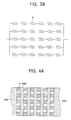
- FIG. 3B is a schematic circuit diagram of the segment heaters H shown in FIG. 3A.
- FIG. 4A is a plan view illustrating electrical connections of the segment heaters H in accordance with another embodiment of the present general inventive concept
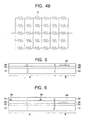
- FIG. 4B is a schematic circuit diagram of FIG. 4A.
- the segment heaters H may be disposed to form a matrix array having the same number of rows and columns.
- the segment heaters H may be connected to each other in series and/or in parallel. For example, when a driving voltage of the ink jet head is about 10 ⁇ 15 V (volts), the total resistance of the segment heaters H may be adjusted to have a resistance between about 30 and about 200 ⁇ (Ohms). In the embodiment shown in FIGS. 3A and 3B, six segment heaters H connected in series are connected to each other in 6 rows.
- the total resistance of the segment heaters H may be equal to a separate resistance of the segment heaters H.
- the segment heaters H may be connected to each other in parallel by heater wirings 34b'.
- the segment heaters H and the heater wirings 34b may be disposed at the same level as the heat-generating resistors R and the ink ejection wirings 34a, respectively.
- the segment heaters H and the heater wirings 34b may be formed by the same process and formed of the same material as the heat-generating resistors R and the ink ejection wirings 34a, respectively.
- the segment heaters H may be made of any metal selected from a group including tantalum (Ta), tungsten (W), chrome (Cr), molybdenum (Mo), titanium (Ti), zirconium (Zr) and hafnium (Hf), or an alloy including the selected metal.
- other materials may also be used to make the segment heaters.
- the heater wirings 34b may be made of aluminum.
- the plurality of segment heaters H having an area substantially equal to the heat-generating resistors R and are formed in the same process as the heat-generating resistors R. Therefore, as can be seen from the following description, it is possible to prevent reliability of the process from deteriorating due to an area difference between the heat-generating resistors and the substrate heaters caused by the segment heaters having a wider area than that of the heat-generating resistors.
- the plurality of segment heaters H is combined to constitute the substrate heater, thereby facilitating adjustment of a total resistance of the substrate heater.
- a line-shaped temperature sensing line 28, which is buried in the upper interlayer insulating layer 30, may be disposed on the intermediate interlayer insulating layer 26 to be located adjacent to the pressure-generating elements. Each end of the temperature sensing line 28 is connected to the conductive pads 14.
- the temperature sensing line may be made of aluminum. As shown in FIG. 1, the temperature sensing line 28 is disposed adjacent to the heat-generating resistors R. Therefore, the substrate temperature of the ink ejection region 12a from which the ink is actually ejected may be more precisely detected.
- the temperature sensing line 28 may be omitted, and the intermediate interlayer insulating layer may also be omitted.
- the temperature of the substrate 12 may be measured by forming a diode type temperature sensor in the substrate 12 of the logic circuit regions 12c or forming a heat resistant device, such as aluminum, on the interlayer insulating layer of the logic circuit regions 12c.
- a passivation layer 36 that covers the heat-generating resistors R, the ink ejection wirings 34a, the segment heaters H, and the heater wirings 34b is disposed on the upper interlayer insulating layer 30.
- the passivation layer 36 functions to prevent the heat-generating resistors R, the ink ejection wirings 34a, the segment heaters H, and the heater wirings 34b from corroding due to contact with the ink or exposure to air.
- the passivation layer 36 may be formed of a silicon nitride layer.
- an anti-cavitation layer 38 is disposed on the passivation layer 36 to at least overlap with the heat-generating resistors R.
- the anti-cavitation layer 38 may be made of tantalum.
- An ink-supply passage 40 which passes through the substrate 12, the interlayer insulating layers 22, 26 and 30, and the passivation layer 36, is disposed in the ink ejection region 12a.
- the ink-supply passage 40 may be disposed between the heat-generating resistors R arranged in two rows.
- the temperature sensing line 28 may be disposed between the heat-generating resistors R and the ink-supply passage 40, when viewed in a plan view.
- the ink flow path includes a plurality of ink chambers 46l having the heat-generating resistors R therein, and ink channels 46C in fluid communication with the ink chambers 46I.
- the flow path forming body 42 includes a chamber layer 42a that defines sidewalls of the ink flow path, and a nozzle layer 42b disposed on the chamber layer 42a to cover at least the ink ejection region 12a.
- nozzles 44 corresponding to the heat-generating resistors R are disposed to pass through the nozzle layer 42b.
- the method of manufacturing an ink jet head includes a process of manufacturing the ink jet head substrate 10 and a process of forming the flow path forming body 42 on the ink jet head substrate 10.
- the process of manufacturing the ink jet head substrate 10 will be described with reference to FIGS. 5 to 8 sequentially, and then the process of forming the flow path forming body 42 will be described with reference to FIG. 9.
- MOS transistors may be formed on the substrate 12.
- the MOS transistors may be located in power transistor regions (12b in FIG. 1) and logic circuit regions (12c in FIG. 1).
- the lower interlayer insulating layer 22 is formed on the substrate 12.
- the lower interlayer insulating layer 22 insulates the MOS transistor from metal wirings, which are to be formed in the following process.
- the lower interlayer insulating layer 22 may be formed of a silicon oxide layer, a BPSG layer, or a silicon nitride layer.
- a lower wiring 24 is formed on the lower interlayer insulating layer 22. Address lines may also be formed on the address regions (12d in FIG. 1) during the formation of the lower wiring 24.
- the lower wiring 24 is capable of electrically connecting the address line and the CMOS transistors in the logic circuit regions 12c.
- the lower wiring 24 may be formed by forming an aluminum layer on the lower interlayer insulating layer 22 and patterning the aluminum layer.
- An intermediate interlayer insulating layer 26 may be formed on the substrate 12 having the lower wiring 24.
- the intermediate interlayer insulating layer 26 may be formed of a silicon oxide layer or a BPSG layer.
- a temperature sensing line 28 may be formed on the intermediate interlayer insulating layer 26.
- the temperature sensing line 28 may be formed by forming an aluminum layer on the intermediate interlayer insulating layer 26 and then patterning the aluminum layer.
- the temperature sensing line 28 may be formed to have a line shape along the ink ejection region 12a.
- an upper interlayer insulating layer 30 is formed on the substrate 12 having the temperature sensing line 28.
- the upper interlayer insulating layer 30 may be formed of a silicon oxide layer or a BPSG layer.
- the process of forming the temperature sensing line 28 may be omitted, and the process of forming the intermediate interlayer insulating layer 26 may also be omitted.
- the upper interlayer insulating layer 30 may be directly formed on the lower interlayer insulating layer 22 to cover the lower wiring 24.
- the high resistance metal layer 32 may be made of a metal layer or an alloy layer including a material selected from a group including tantalum (Ta), tungsten (W), chrome (Cr), molybdenum (Mo), titanium (Ti), zirconium (Zr) and hafnium (Hf). Other materials may also be used to make the high resistance metal layer.
- the metal wiring layer 34 may be formed of a material layer having a resistance lower than that of the high resistance metal layer 32. For example, the metal wiring layer 34 may be formed of an aluminum layer by a sputtering method.
- the metal wiring layer pattern is selectively removed to form ink ejection wirings 34a and heater wirings 34b in order to expose a predetermined region of the high resistance metal layer pattern 32'.
- the metal wiring layer pattern may be removed by photo and wet etching processes.
- the high resistance metal layer pattern 32' exposed by the ink ejection wirings 34a is provided as the heat-generating resistors R, and the high resistance metal layer pattern 32' exposed by the heater wirings 34b is provided as the segment heaters H.
- conductive pads 14 may be formed together on the upper interlayer insulating layer 30 of the both ends of the substrate 12.
- the ink ejection wirings 34a which are connected to one side of the heat-generating resistors R, may be electrically connected to source and drain regions of the MOS transistor formed on the substrate of the power transistor regions (12b in FIG. 1) by a conductive contact structure (not shown) passing through the interlayer insulating layers 22, 26 and 30 on the power transistor regions (12b in FIG. 1).
- the ink ejection wirings 34a which are connected to the other side of the heat-generating resistors R, may be directly connected to the conductive pads 14.
- the heater wirings 34b may be also directly connected to the conductive pads 14.
- the heat-generating resistors R are formed to have a predetermined array in the ink ejection region (12a in FIG. 1).
- the segment heaters H may be formed to be disposed in a matrix array on the logic circuit region (12c in FIG. 1).
- the segment heaters H are formed to have an area substantially equal to the heat-generating resistors R.
- the segment heaters H that have an area substantially equal to the heat-generating resistors R may be formed by the same wet etching process as the heat-generating resistors R. Therefore, unlike the conventional substrate heaters having an area wider than that of the heat-generating resistors, embodiments of the present invention are capable of preventing deterioration of the reliability of the substrate heaters formed by the same wet etching process as the heat-generating resistors.
- a passivation layer 36 covering the heat-generating resistors R, the segment heaters H, the ink ejection wirings 34a, and the heater wirings 34b is formed.
- the passivation layer 36 may be formed of a silicon nitride layer.
- the anti-cavitation layer 38 may be formed by forming a tantalum layer on the passivation layer 36 and then patterning the tantalum layer.
- the flow path forming body 42 provided with nozzles 44 is formed on the substrate 12, at which the anti-cavitation layer 38 is formed.
- the ink flow path including ink chambers 46l having the heat-generating resistors R therein and ink channels 46C in fluid communication with the ink chambers are defined by the flow path forming body 42.
- the flow path forming body 42 includes a chamber layer 42a forming sidewalls of the ink flow path and a nozzle layer 42b formed on the chamber layer 42a to cover at least the ink ejection region (12a in FIG. 1).
- the flow path forming body 42 may be formed by various methods according to technologies known to those skilled in the art. In accordance with an embodiment of the present invention, the flow path forming body may be formed by the following process.
- a negative photoresist layer is formed on the substrate 12 having the anti-cavitation layer 38.
- the negative photoresist layer is patterned by exposure and development processes to form the chamber layer 42a.
- a sacrificial layer that fills between the chamber layers 42a is formed, and the nozzle layer 42b is formed on the chamber layer 42a and the sacrificial layer.
- the nozzle layer 42b may be formed of the negative photoresist layer.
- the nozzle layer 42b is patterned by the exposure and development processes to form the nozzles 44.
- the substrate 12 having the nozzles is etched from the rear surface to form an ink-supply passage 40.
- the interlayer insulating layers 22, 26 and 30 are etched together.
- the sacrificial layer is removed to form the ink chambers 46I and the ink channels 46C at the region where the sacrificial layer is removed.
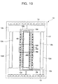
- FIG. 10 is a plan view of an ink jet head in accordance with another embodiment of the present invention
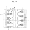
- FIG. 11 is an enlarged plan view of a portion R2 of an ink ejection region shown in FIG. 10.
- FIGS. 12 to 15 are cross-sectional views, taken along the line 11I - 11I' of FIG. 11, illustrating a method of manufacturing an ink jet head in accordance with another embodiment of the present invention.
- lines C-C are corresponding to a corner portion C in FIG. 11.
- descriptions of members designated by the same reference numeral as an embodiment of the present invention described in FIGS. 1 to 9 may be similarly applied to the description of the FIGS. 10 to 15. Therefore, their description will be omitted.
- segment heaters H' may be disposed adjacent to pressure-generating elements R.
- the segment heaters H' disposed along an array of the pressure-generating elements R may be variously changed, but are not limited to, the number and arrangement in consideration of a total resistance of the segment heaters H'.
- the segment heaters H' are electrically connected to each other by heater wirings 134, and ends of the heater wirings 134 are electrically connected to the conductive pads 14, respectively.
- the segment heaters H' and the heater wirings 134 are disposed at a different level from the heat-generating resistors R and the ink ejection wirings 34a in order to insulate against the heat-generating resistors R and the ink ejection wirings 34a.
- the segment heaters H' and the heater wirings 134 may be disposed on the lower interlayer insulating layer 22, and the heat-generating resistors R and the ink ejection wirings 34a may be disposed on the upper interlayer insulating layer 30. While the ink ejection wirings 34a are omitted in FIG. 11 to clearly illustrate the segment heaters H' and the heater wirings 134, the ink ejection wirings 34a shown in FIG. 2 may be applied to have the same arrangement as FIG. 11.
- the segment heaters H' have an area substantially equal to the heat-generating resistors R. However, in accordance with another embodiment of the present invention, since the segment heaters H' and the heat-generating resistors R are formed at a different level by a separate process, area and shape of the segment heaters H' may be modified on more relaxed conditions.
- the temperature sensing line 28 and the segment heaters H' may be spaced apart from each other with the heat-generating resistors R interposed between them, when viewed in a plan view.
- the segment heaters H' may be disposed adjacent to the heat-generating resistors R to be uniformly distributed on the substrate 12. As a result, it becomes possible to uniformly heat the substrate 12.
- the segment heaters H' may be disposed in the vicinity of the heat-generating resistors R to uniformly heat the substrate 12 at a portion where the ink is actually ejected, thereby preventing performance of the ink ejection during an initial printing operation from deteriorating.
- a lower interlayer insulating layer 22 is formed on a substrate 12.
- Segment heaters H' and heater wirings 134 that electrically connect the segment heaters H' to each other are formed on the lower interlayer insulating layer 22.
- the segment heaters H' and the heater wirings 134 may be formed by the following process.
- a heater material layer and a heater-wiring layer are sequentially formed on the lower interlayer insulating layer 22.
- the heater material layer may be made of a metal layer or an alloy layer including any material selected from a group including tantalum (Ta), tungsten (W), chrome (Cr), molybdenum (Mo), titanium (Ti), zirconium (Zr) and hafnium (Hf).
- the heater-wiring layer may be formed of a material layer such as an aluminum layer having a resistance lower than that of the heater material layer. Then, the heater-wiring layer and the heater material layer are patterned to form a heater pattern.
- the heater pattern includes a heater material layer pattern 132 and a heater-wiring layer pattern, which are sequentially stacked.
- the heater pattern may be formed to have a line shape along an ink ejection region (12a in FIG. 10).
- the heater-wiring layer pattern is selectively removed by performing photo and wet etching processes to form the heater wirings 134.
- the heater material layer pattern 132 at a portion exposed by the heater wirings 134 is provided as the segment heaters H'. In this process, address lines may be formed together at address line regions 12d.
- an alternative intermediate interlayer insulating layer 26 may be formed on the substrate 12 having the segment heaters H' and the heater wirings 134 thereon.
- a temperature sensing line 28 may be formed on the intermediate interlayer insulating layer 26 by using an aluminum layer. Alternatively, a process of forming the temperature sensing line 28 may be omitted. In this case, a process of forming the intermediate interlayer insulating layer 26 may be also omitted.
- An upper interlayer insulating layer 30 is formed on the substrate 12 having the temperature sensing line 28 thereon. When the process of forming the temperature sensing line 28 is omitted, the upper interlayer insulating layer 30 may be directly formed on the lower interlayer insulating layer 22 to cover the segment heaters H' and the heater wirings 134.
- heat-generating resistors R and ink ejection wirings 34a are formed on the upper interlayer insulating layer 30.
- the heat-generating resistors R and the ink ejection wirings 34a may be formed by the following process.
- a high resistance metal layer and a metal wiring layer are sequentially formed on the upper interlayer insulating layer 30.
- the high resistance metal layer may be formed of the same material layer as the heater material layer.
- the high resistance metal layer may be made of a metal layer or an alloy layer including any material selected from a group including tantalum (Ta), tungsten (W), chrome (Cr), molybdenum (Mo), titanium (Ti), zirconium (Zr) and hafnium (Hf).
- the metal wiring layer may be made of an aluminum layer. Then, the metal wiring layer and the high resistance metal layer are patterned to form an ink ejection pattern.
- the ink ejection pattern includes a high resistance metal layer pattern 32' and a metal wiring layer pattern, which are sequentially stacked. Then, the metal wiring layer pattern is selectively removed to form the ink ejection wirings 34a.
- the high resistance metal layer pattern at a portion exposed by the ink ejection wirings 34a is provided as the heat-generating resistors R.
- the heat-generating resistors R are formed adjacent to the segment heaters H' in the ink ejection region (12a in FIG. 10).
- a passivation layer 36 that covers the heat-generating resistors R and the ink ejection wirings 34a is formed on the upper interlayer insulating layer 30.
- An anti-cavitation layer 38 is then formed on the passivation layer 36 to at least overlap with the heat-generating resistors R.
- an ink-supply passage 40 and a flow path forming body 42 are formed by performing the process described in FIG. 9.
- embodiments of the present invention provide a plurality of segment heaters as a substrate-heating member that heat a substrate.
- the process of forming the segment heaters may be combined to the process of forming the pressure-generating elements that generate pressure to eject ink to simplify the entire process, thereby improving reliability of the segment heaters.
- the segment heaters may be uniformly distributed on the substrate in comparison with the conventional substrate heater having a wide area. As a result, it becomes possible to uniformly heat the substrate.
- the segment heaters are disposed adjacent to the pressure-generating element that actually eject the ink, thereby preventing performance of the ink ejection during an initial printing operation from deteriorating.
Landscapes
- Engineering & Computer Science (AREA)
- Manufacturing & Machinery (AREA)
- Particle Formation And Scattering Control In Inkjet Printers (AREA)
Applications Claiming Priority (2)
| Application Number | Priority Date | Filing Date | Title |
|---|---|---|---|
| KR1020040056961A KR100757861B1 (ko) | 2004-07-21 | 2004-07-21 | 잉크젯 헤드 기판, 잉크젯 헤드 및 잉크젯 헤드 기판의제조방법. |
| EP05254495A EP1621347B1 (fr) | 2004-07-21 | 2005-07-20 | Substrat de tête à jet d'encre, tête à jet d'encre, et procédé de la fabrication d'un substrat |
Related Parent Applications (1)
| Application Number | Title | Priority Date | Filing Date |
|---|---|---|---|
| EP05254495A Division EP1621347B1 (fr) | 2004-07-21 | 2005-07-20 | Substrat de tête à jet d'encre, tête à jet d'encre, et procédé de la fabrication d'un substrat |
Publications (3)
| Publication Number | Publication Date |
|---|---|
| EP1920930A2 true EP1920930A2 (fr) | 2008-05-14 |
| EP1920930A3 EP1920930A3 (fr) | 2008-05-28 |
| EP1920930B1 EP1920930B1 (fr) | 2009-01-14 |
Family
ID=35219260
Family Applications (2)
| Application Number | Title | Priority Date | Filing Date |
|---|---|---|---|
| EP07122521A Expired - Lifetime EP1920930B1 (fr) | 2004-07-21 | 2005-07-20 | Substrat de tête à jet d'encre, tête à jet d'encre et procédé de fabrication d'un substrat de tête à jet d'encre |
| EP05254495A Expired - Lifetime EP1621347B1 (fr) | 2004-07-21 | 2005-07-20 | Substrat de tête à jet d'encre, tête à jet d'encre, et procédé de la fabrication d'un substrat |
Family Applications After (1)
| Application Number | Title | Priority Date | Filing Date |
|---|---|---|---|
| EP05254495A Expired - Lifetime EP1621347B1 (fr) | 2004-07-21 | 2005-07-20 | Substrat de tête à jet d'encre, tête à jet d'encre, et procédé de la fabrication d'un substrat |
Country Status (6)
| Country | Link |
|---|---|
| US (1) | US7470000B2 (fr) |
| EP (2) | EP1920930B1 (fr) |
| JP (1) | JP2006027274A (fr) |
| KR (1) | KR100757861B1 (fr) |
| CN (1) | CN100364771C (fr) |
| DE (2) | DE602005004335T2 (fr) |
Families Citing this family (28)
| Publication number | Priority date | Publication date | Assignee | Title |
|---|---|---|---|---|
| US20060081239A1 (en) * | 2004-10-15 | 2006-04-20 | Alley Rodney L | Thermally efficient drop generator |
| KR100620377B1 (ko) * | 2004-11-12 | 2006-09-07 | 삼성전자주식회사 | 동시토출이 가능한 잉크젯 프린트헤드 |
| JP2007290361A (ja) * | 2006-03-31 | 2007-11-08 | Canon Inc | 液体吐出ヘッド及びそれを用いた液体吐出装置 |
| JP4953703B2 (ja) * | 2006-06-19 | 2012-06-13 | キヤノン株式会社 | 記録装置及びインク吐出不良検出方法 |
| JP4804251B2 (ja) * | 2006-07-20 | 2011-11-02 | キヤノン株式会社 | 撮像装置及び撮像ユニット |
| JP4799389B2 (ja) * | 2006-12-14 | 2011-10-26 | キヤノン株式会社 | ヘッド基板、記録ヘッド、ヘッドカートリッジ、及び記録装置 |
| KR20090024380A (ko) * | 2007-09-04 | 2009-03-09 | 삼성전자주식회사 | 잉크젯 프린트 헤드 |
| TWI332904B (en) | 2007-11-29 | 2010-11-11 | Internat United Technology Company Ltd | Thermal inkjet printhead chip structure and manufacture method thereof |
| US7989144B2 (en) | 2008-04-01 | 2011-08-02 | Az Electronic Materials Usa Corp | Antireflective coating composition |
| KR101313946B1 (ko) * | 2008-08-29 | 2013-10-01 | 캐논 가부시끼가이샤 | 액체 토출 헤드용 기판, 그 제조 방법 및 액체 토출 헤드 |
| US8083323B2 (en) | 2008-09-29 | 2011-12-27 | Xerox Corporation | On-chip heater and thermistors for inkjet |
| US8455176B2 (en) * | 2008-11-12 | 2013-06-04 | Az Electronic Materials Usa Corp. | Coating composition |
| US20100119979A1 (en) * | 2008-11-13 | 2010-05-13 | Rahman M Dalil | Antireflective Coating Composition Comprising Fused Aromatic Rings |
| US20100119980A1 (en) * | 2008-11-13 | 2010-05-13 | Rahman M Dalil | Antireflective Coating Composition Comprising Fused Aromatic Rings |
| US7988260B2 (en) * | 2008-11-20 | 2011-08-02 | Canon Kabushiki Kaisha | Recording element substrate and recording head including recording element substrate |
| US20100151392A1 (en) * | 2008-12-11 | 2010-06-17 | Rahman M Dalil | Antireflective coating compositions |
| US8876242B2 (en) * | 2009-05-08 | 2014-11-04 | Canon Kabushiki Kaisha | Liquid ejection head |
| US20100316949A1 (en) * | 2009-06-10 | 2010-12-16 | Rahman M Dalil | Spin On Organic Antireflective Coating Composition Comprising Polymer with Fused Aromatic Rings |
| US8486609B2 (en) * | 2009-12-23 | 2013-07-16 | Az Electronic Materials Usa Corp. | Antireflective coating composition and process thereof |
| US9931840B2 (en) * | 2013-08-22 | 2018-04-03 | Xerox Corporation | Systems and methods for heating and measuring temperature of print head jet stacks |
| EP3470228B1 (fr) * | 2017-10-11 | 2021-06-30 | Canon Kabushiki Kaisha | Substrat d'élément, son procédé de fabrication, tête d'impression et imprimante |
| JP6552692B2 (ja) * | 2018-08-06 | 2019-07-31 | キヤノン株式会社 | 素子基板、液体吐出ヘッド、及び記録装置 |
| JP7346150B2 (ja) * | 2019-08-09 | 2023-09-19 | キヤノン株式会社 | インクジェット記録ヘッドおよびインクジェット記録装置 |
| WO2021066805A1 (fr) * | 2019-09-30 | 2021-04-08 | Hewlett-Packard Development Company, L.P. | Éjection de fluide avec ajustements d'éjection |
| CN113211985B (zh) * | 2020-01-21 | 2022-10-14 | 国际联合科技股份有限公司 | 热气泡喷墨头装置 |
| US11571896B2 (en) * | 2021-02-01 | 2023-02-07 | Funai Electric Co., Ltd. | Customization of multichannel printhead |
| JP7683371B2 (ja) * | 2021-07-14 | 2025-05-27 | セイコーエプソン株式会社 | 液体吐出ヘッドユニットおよび液体吐出装置 |
| JP7764173B2 (ja) * | 2021-09-17 | 2025-11-05 | キヤノン株式会社 | 液体吐出ヘッド |
Citations (1)
| Publication number | Priority date | Publication date | Assignee | Title |
|---|---|---|---|---|
| US5175565A (en) | 1988-07-26 | 1992-12-29 | Canon Kabushiki Kaisha | Ink jet substrate including plural temperature sensors and heaters |
Family Cites Families (29)
| Publication number | Priority date | Publication date | Assignee | Title |
|---|---|---|---|---|
| US637863A (en) * | 1899-03-17 | 1899-11-28 | John A Gavin | Ventilator. |
| DE3705014A1 (de) | 1986-02-18 | 1987-08-20 | Canon Kk | Tintenstrahl-aufzeichnungskopf und substrat hierfuer |
| US6234599B1 (en) * | 1988-07-26 | 2001-05-22 | Canon Kabushiki Kaisha | Substrate having a built-in temperature detecting element, and ink jet apparatus having the same |
| JP2806562B2 (ja) * | 1988-07-26 | 1998-09-30 | キヤノン株式会社 | 液体噴射記録ヘッド,該記録ヘッドを有する記録装置および液体噴射記録ヘッドの駆動方法 |
| JP2831778B2 (ja) | 1989-02-03 | 1998-12-02 | キヤノン株式会社 | 液体噴射記録ヘッド、該記録ヘッド用基板および記録装置 |
| JPH0363137A (ja) | 1989-08-02 | 1991-03-19 | Canon Inc | インクジェット記録ヘッド |
| JP2815959B2 (ja) | 1990-02-19 | 1998-10-27 | キヤノン株式会社 | 液体噴射記録装置 |
| US6116710A (en) * | 1991-01-18 | 2000-09-12 | Canon Kabushiki Kaisha | Ink jet recording method and apparatus using thermal energy |
| JPH05175565A (ja) * | 1991-12-19 | 1993-07-13 | Omron Corp | 圧電アクチュエータの駆動方法 |
| US5734392A (en) | 1995-09-14 | 1998-03-31 | Lexmark International, Inc. | Ink jet printhead heating during margin periods |
| US5774148A (en) * | 1995-10-19 | 1998-06-30 | Lexmark International, Inc. | Printhead with field oxide as thermal barrier in chip |
| JPH10774A (ja) * | 1996-06-14 | 1998-01-06 | Canon Inc | インクジェット記録ヘッド用基板及びこれを備えたインクジェット記録ヘッド |
| US6102515A (en) | 1997-03-27 | 2000-08-15 | Lexmark International, Inc. | Printhead driver for jetting heaters and substrate heater in an ink jet printer and method of controlling such heaters |
| JPH11115173A (ja) | 1997-07-11 | 1999-04-27 | Lexmark Internatl Inc | 一体的な基板ヒータ・ドライバを有する印刷ヘッドを具備したインクジェットプリンタ |
| US6139131A (en) | 1999-08-30 | 2000-10-31 | Hewlett-Packard Company | High drop generator density printhead |
| US6357863B1 (en) | 1999-12-02 | 2002-03-19 | Lexmark International Inc. | Linear substrate heater for ink jet print head chip |
| TW446644B (en) * | 2000-01-29 | 2001-07-21 | Ind Tech Res Inst | Method and structure for precise temperature measurement of ink-jet printhead heating element |
| US6620503B2 (en) * | 2000-07-26 | 2003-09-16 | Kimberly-Clark Worldwide, Inc. | Synthetic fiber nonwoven web and method |
| JP4510259B2 (ja) * | 2000-09-28 | 2010-07-21 | キヤノン株式会社 | 記録装置及び温度推定方法 |
| KR100408280B1 (ko) | 2001-01-10 | 2003-12-01 | 삼성전자주식회사 | 잉크 젯 프린터에서 헤드 기판의 온도 보상 장치 및 방법 |
| JP2002370363A (ja) * | 2001-06-15 | 2002-12-24 | Canon Inc | インクジェット記録ヘッド用基板、インクジェット記録ヘッド、インクジェット記録装置 |
| US6896360B2 (en) * | 2002-10-31 | 2005-05-24 | Hewlett-Packard Development Company, L.P. | Barrier feature in fluid channel |
| US6755509B2 (en) * | 2002-11-23 | 2004-06-29 | Silverbrook Research Pty Ltd | Thermal ink jet printhead with suspended beam heater |
| KR100470570B1 (ko) | 2002-12-18 | 2005-03-09 | 삼성전자주식회사 | 잉크젯 프린터 헤드칩 |
| KR100567026B1 (ko) * | 2002-12-24 | 2006-04-04 | 매그나칩 반도체 유한회사 | 얕은 트렌치 아이솔레이션 코너의 모우트 개선방법 |
| TWI246462B (en) * | 2003-06-10 | 2006-01-01 | Canon Kk | Ink-jet printhead substrate, driving control method, ink-jet printhead and ink-jet printing apparatus |
| KR20050073093A (ko) * | 2004-01-08 | 2005-07-13 | 삼성전자주식회사 | 온도센서를 갖는 잉크젯 프린트 헤드 및 그것을 제조하는방법 |
| KR100537522B1 (ko) * | 2004-02-27 | 2005-12-19 | 삼성전자주식회사 | 압전 방식의 잉크젯 프린트헤드와 그 노즐 플레이트의제조 방법 |
| US7163272B2 (en) * | 2004-06-10 | 2007-01-16 | Lexmark International, Inc. | Inkjet print head |
-
2004
- 2004-07-21 KR KR1020040056961A patent/KR100757861B1/ko not_active Expired - Fee Related
-
2005
- 2005-01-19 US US11/037,081 patent/US7470000B2/en not_active Expired - Fee Related
- 2005-05-16 CN CNB2005100726739A patent/CN100364771C/zh not_active Expired - Fee Related
- 2005-07-20 DE DE602005004335T patent/DE602005004335T2/de not_active Expired - Lifetime
- 2005-07-20 DE DE602005012441T patent/DE602005012441D1/de not_active Expired - Fee Related
- 2005-07-20 EP EP07122521A patent/EP1920930B1/fr not_active Expired - Lifetime
- 2005-07-20 EP EP05254495A patent/EP1621347B1/fr not_active Expired - Lifetime
- 2005-07-21 JP JP2005211915A patent/JP2006027274A/ja active Pending
Patent Citations (1)
| Publication number | Priority date | Publication date | Assignee | Title |
|---|---|---|---|---|
| US5175565A (en) | 1988-07-26 | 1992-12-29 | Canon Kabushiki Kaisha | Ink jet substrate including plural temperature sensors and heaters |
Also Published As
| Publication number | Publication date |
|---|---|
| DE602005004335D1 (de) | 2008-03-06 |
| EP1920930B1 (fr) | 2009-01-14 |
| DE602005012441D1 (de) | 2009-03-05 |
| CN1724257A (zh) | 2006-01-25 |
| DE602005004335T2 (de) | 2009-01-15 |
| EP1621347A2 (fr) | 2006-02-01 |
| CN100364771C (zh) | 2008-01-30 |
| JP2006027274A (ja) | 2006-02-02 |
| EP1920930A3 (fr) | 2008-05-28 |
| EP1621347A3 (fr) | 2006-06-07 |
| KR100757861B1 (ko) | 2007-09-11 |
| US20060017774A1 (en) | 2006-01-26 |
| EP1621347B1 (fr) | 2008-01-16 |
| US7470000B2 (en) | 2008-12-30 |
| KR20060007730A (ko) | 2006-01-26 |
Similar Documents
| Publication | Publication Date | Title |
|---|---|---|
| EP1920930B1 (fr) | Substrat de tête à jet d'encre, tête à jet d'encre et procédé de fabrication d'un substrat de tête à jet d'encre | |
| JP6270358B2 (ja) | 液体吐出ヘッド | |
| KR100560593B1 (ko) | 액체 토출 헤드의 제조방법 | |
| US9242460B2 (en) | Liquid-discharge-head substrate, method of manufacturing the same, and liquid discharge head | |
| CA2631454C (fr) | Dispositif d'ejection de microfluide a faible consommation d'energie et a longue duree de vie | |
| EP1352744B1 (fr) | Distributeur de liquide et imprimante | |
| JP7112287B2 (ja) | 素子基板、記録ヘッド、記録装置、及び素子基板の製造方法 | |
| JP3326152B2 (ja) | プリントヘッド装置 | |
| US11524497B2 (en) | Liquid discharge head and liquid discharge device | |
| JP5222005B2 (ja) | 記録ヘッドの製造方法 | |
| US9061500B2 (en) | Printhead substrate, method of manufacturing the same, printhead, and printing apparatus | |
| JP4137257B2 (ja) | サーマルインクジェットプリントヘッド及びその製造方法 | |
| US7367657B2 (en) | Inkjet printhead with transistor driver | |
| KR20050073093A (ko) | 온도센서를 갖는 잉크젯 프린트 헤드 및 그것을 제조하는방법 | |
| KR20040055230A (ko) | 잉크젯 프린트헤드 및 그 제조방법 | |
| RU2826125C1 (ru) | Печатающая головка для термографической струйной печати, а также печатающий узел и печатающее устройство, содержащие ее | |
| KR100522603B1 (ko) | 모놀리틱 잉크젯 프린트헤드 및 그 제조방법 | |
| CN100368202C (zh) | 喷墨打印头芯片 | |
| KR20220143755A (ko) | 열 잉크젯 프린트헤드 및 이를 포함하는 인쇄 어셈블리 및 인쇄 장치 | |
| KR20060006657A (ko) | 잉크젯 프린트 헤드 및 그것을 제조하는 방법 | |
| KR100497389B1 (ko) | 잉크젯 프린트헤드 및 그 제조방법 |
Legal Events
| Date | Code | Title | Description |
|---|---|---|---|
| PUAI | Public reference made under article 153(3) epc to a published international application that has entered the european phase |
Free format text: ORIGINAL CODE: 0009012 |
|
| PUAL | Search report despatched |
Free format text: ORIGINAL CODE: 0009013 |
|
| 17P | Request for examination filed |
Effective date: 20071206 |
|
| AC | Divisional application: reference to earlier application |
Ref document number: 1621347 Country of ref document: EP Kind code of ref document: P |
|
| AK | Designated contracting states |
Kind code of ref document: A2 Designated state(s): DE FR GB NL |
|
| AK | Designated contracting states |
Kind code of ref document: A3 Designated state(s): DE FR GB NL |
|
| GRAP | Despatch of communication of intention to grant a patent |
Free format text: ORIGINAL CODE: EPIDOSNIGR1 |
|
| GRAS | Grant fee paid |
Free format text: ORIGINAL CODE: EPIDOSNIGR3 |
|
| GRAA | (expected) grant |
Free format text: ORIGINAL CODE: 0009210 |
|
| AC | Divisional application: reference to earlier application |
Ref document number: 1621347 Country of ref document: EP Kind code of ref document: P |
|
| AK | Designated contracting states |
Kind code of ref document: B1 Designated state(s): DE FR GB NL |
|
| REG | Reference to a national code |
Ref country code: GB Ref legal event code: FG4D |
|
| AKX | Designation fees paid |
Designated state(s): DE FR GB NL |
|
| REF | Corresponds to: |
Ref document number: 602005012441 Country of ref document: DE Date of ref document: 20090305 Kind code of ref document: P |
|
| PG25 | Lapsed in a contracting state [announced via postgrant information from national office to epo] |
Ref country code: NL Free format text: LAPSE BECAUSE OF FAILURE TO SUBMIT A TRANSLATION OF THE DESCRIPTION OR TO PAY THE FEE WITHIN THE PRESCRIBED TIME-LIMIT Effective date: 20090114 |
|
| NLV1 | Nl: lapsed or annulled due to failure to fulfill the requirements of art. 29p and 29m of the patents act | ||
| PLBE | No opposition filed within time limit |
Free format text: ORIGINAL CODE: 0009261 |
|
| STAA | Information on the status of an ep patent application or granted ep patent |
Free format text: STATUS: NO OPPOSITION FILED WITHIN TIME LIMIT |
|
| 26N | No opposition filed |
Effective date: 20091015 |
|
| GBPC | Gb: european patent ceased through non-payment of renewal fee |
Effective date: 20090720 |
|
| REG | Reference to a national code |
Ref country code: FR Ref legal event code: ST Effective date: 20100331 |
|
| PG25 | Lapsed in a contracting state [announced via postgrant information from national office to epo] |
Ref country code: FR Free format text: LAPSE BECAUSE OF NON-PAYMENT OF DUE FEES Effective date: 20090731 |
|
| PG25 | Lapsed in a contracting state [announced via postgrant information from national office to epo] |
Ref country code: GB Free format text: LAPSE BECAUSE OF NON-PAYMENT OF DUE FEES Effective date: 20090720 |
|
| PG25 | Lapsed in a contracting state [announced via postgrant information from national office to epo] |
Ref country code: DE Free format text: LAPSE BECAUSE OF NON-PAYMENT OF DUE FEES Effective date: 20100202 |