EP1921084B1 - Polmerisierbare Diazoniumsalze, Verfahren zu deren Herstellung und deren Verwendung - Google Patents
Polmerisierbare Diazoniumsalze, Verfahren zu deren Herstellung und deren Verwendung Download PDFInfo
- Publication number
- EP1921084B1 EP1921084B1 EP07290888A EP07290888A EP1921084B1 EP 1921084 B1 EP1921084 B1 EP 1921084B1 EP 07290888 A EP07290888 A EP 07290888A EP 07290888 A EP07290888 A EP 07290888A EP 1921084 B1 EP1921084 B1 EP 1921084B1
- Authority
- EP
- European Patent Office
- Prior art keywords
- diazonium
- diazonium salt
- bipyridine
- diazonium salts
- redox
- Prior art date
- Legal status (The legal status is an assumption and is not a legal conclusion. Google has not performed a legal analysis and makes no representation as to the accuracy of the status listed.)
- Active
Links
- 239000012954 diazonium Substances 0.000 title claims abstract description 123
- 150000001989 diazonium salts Chemical class 0.000 title claims description 102
- 238000004519 manufacturing process Methods 0.000 title description 6
- 238000000034 method Methods 0.000 claims abstract description 40
- 229920000642 polymer Polymers 0.000 claims abstract description 32
- VQGHOUODWALEFC-UHFFFAOYSA-N 2-phenylpyridine Chemical compound C1=CC=CC=C1C1=CC=CC=N1 VQGHOUODWALEFC-UHFFFAOYSA-N 0.000 claims abstract description 22
- ROFVEXUMMXZLPA-UHFFFAOYSA-N Bipyridyl Chemical compound N1=CC=CC=C1C1=CC=CC=N1 ROFVEXUMMXZLPA-UHFFFAOYSA-N 0.000 claims abstract description 18
- 239000003446 ligand Substances 0.000 claims abstract description 17
- JUJWROOIHBZHMG-UHFFFAOYSA-N Pyridine Chemical compound C1=CC=NC=C1 JUJWROOIHBZHMG-UHFFFAOYSA-N 0.000 claims abstract description 16
- 229920006254 polymer film Polymers 0.000 claims abstract description 14
- 239000000758 substrate Substances 0.000 claims abstract description 14
- 238000010521 absorption reaction Methods 0.000 claims abstract description 13
- 229910052707 ruthenium Inorganic materials 0.000 claims abstract description 12
- 229910052741 iridium Inorganic materials 0.000 claims abstract description 11
- JVZRCNQLWOELDU-UHFFFAOYSA-N gamma-Phenylpyridine Natural products C1=CC=CC=C1C1=CC=NC=C1 JVZRCNQLWOELDU-UHFFFAOYSA-N 0.000 claims abstract description 10
- 230000008569 process Effects 0.000 claims abstract description 9
- UMJSCPRVCHMLSP-UHFFFAOYSA-N pyridine Natural products COC1=CC=CN=C1 UMJSCPRVCHMLSP-UHFFFAOYSA-N 0.000 claims abstract description 8
- JFJNVIPVOCESGZ-UHFFFAOYSA-N 2,3-dipyridin-2-ylpyridine Chemical compound N1=CC=CC=C1C1=CC=CN=C1C1=CC=CC=N1 JFJNVIPVOCESGZ-UHFFFAOYSA-N 0.000 claims abstract description 5
- DGEZNRSVGBDHLK-UHFFFAOYSA-N [1,10]phenanthroline Chemical compound C1=CN=C2C3=NC=CC=C3C=CC2=C1 DGEZNRSVGBDHLK-UHFFFAOYSA-N 0.000 claims abstract description 4
- 239000002356 single layer Substances 0.000 claims abstract description 4
- 229910052723 transition metal Inorganic materials 0.000 claims abstract description 3
- 150000003624 transition metals Chemical class 0.000 claims abstract description 3
- -1 unsaturated C1-C5-alkyl spacer compound Chemical class 0.000 claims description 35
- 239000004065 semiconductor Substances 0.000 claims description 33
- 229910052710 silicon Inorganic materials 0.000 claims description 27
- 239000010703 silicon Substances 0.000 claims description 27
- 239000010410 layer Substances 0.000 claims description 26
- RAXXELZNTBOGNW-UHFFFAOYSA-N imidazole Natural products C1=CNC=N1 RAXXELZNTBOGNW-UHFFFAOYSA-N 0.000 claims description 21
- 150000004696 coordination complex Chemical class 0.000 claims description 18
- BASFCYQUMIYNBI-UHFFFAOYSA-N platinum Chemical compound [Pt] BASFCYQUMIYNBI-UHFFFAOYSA-N 0.000 claims description 16
- KJTLSVCANCCWHF-UHFFFAOYSA-N Ruthenium Chemical compound [Ru] KJTLSVCANCCWHF-UHFFFAOYSA-N 0.000 claims description 14
- 210000004027 cell Anatomy 0.000 claims description 14
- SIKJAQJRHWYJAI-UHFFFAOYSA-N Indole Chemical compound C1=CC=C2NC=CC2=C1 SIKJAQJRHWYJAI-UHFFFAOYSA-N 0.000 claims description 12
- RWRDLPDLKQPQOW-UHFFFAOYSA-N Pyrrolidine Chemical compound C1CCNC1 RWRDLPDLKQPQOW-UHFFFAOYSA-N 0.000 claims description 12
- XEEYBQQBJWHFJM-UHFFFAOYSA-N Iron Chemical compound [Fe] XEEYBQQBJWHFJM-UHFFFAOYSA-N 0.000 claims description 11
- GKOZUEZYRPOHIO-UHFFFAOYSA-N iridium atom Chemical compound [Ir] GKOZUEZYRPOHIO-UHFFFAOYSA-N 0.000 claims description 10
- 239000000203 mixture Substances 0.000 claims description 10
- 229910052762 osmium Inorganic materials 0.000 claims description 10
- SYQBFIAQOQZEGI-UHFFFAOYSA-N osmium atom Chemical compound [Os] SYQBFIAQOQZEGI-UHFFFAOYSA-N 0.000 claims description 10
- 239000007787 solid Substances 0.000 claims description 10
- 239000007784 solid electrolyte Substances 0.000 claims description 9
- UJOBWOGCFQCDNV-UHFFFAOYSA-N 9H-carbazole Chemical compound C1=CC=C2C3=CC=CC=C3NC2=C1 UJOBWOGCFQCDNV-UHFFFAOYSA-N 0.000 claims description 8
- OKTJSMMVPCPJKN-UHFFFAOYSA-N Carbon Chemical compound [C] OKTJSMMVPCPJKN-UHFFFAOYSA-N 0.000 claims description 8
- YNAVUWVOSKDBBP-UHFFFAOYSA-N Morpholine Chemical compound C1COCCN1 YNAVUWVOSKDBBP-UHFFFAOYSA-N 0.000 claims description 8
- KYQCOXFCLRTKLS-UHFFFAOYSA-N Pyrazine Chemical compound C1=CN=CC=N1 KYQCOXFCLRTKLS-UHFFFAOYSA-N 0.000 claims description 8
- 239000003792 electrolyte Substances 0.000 claims description 8
- 239000002105 nanoparticle Substances 0.000 claims description 8
- 229910052697 platinum Inorganic materials 0.000 claims description 8
- FCEHBMOGCRZNNI-UHFFFAOYSA-N 1-benzothiophene Chemical compound C1=CC=C2SC=CC2=C1 FCEHBMOGCRZNNI-UHFFFAOYSA-N 0.000 claims description 7
- YLQBMQCUIZJEEH-UHFFFAOYSA-N Furan Chemical compound C=1C=COC=1 YLQBMQCUIZJEEH-UHFFFAOYSA-N 0.000 claims description 7
- NQRYJNQNLNOLGT-UHFFFAOYSA-N Piperidine Chemical compound C1CCNCC1 NQRYJNQNLNOLGT-UHFFFAOYSA-N 0.000 claims description 7
- YTPLMLYBLZKORZ-UHFFFAOYSA-N Thiophene Chemical compound C=1C=CSC=1 YTPLMLYBLZKORZ-UHFFFAOYSA-N 0.000 claims description 7
- GLUUGHFHXGJENI-UHFFFAOYSA-N Piperazine Chemical compound C1CNCCN1 GLUUGHFHXGJENI-UHFFFAOYSA-N 0.000 claims description 6
- 229910017052 cobalt Inorganic materials 0.000 claims description 6
- 239000010941 cobalt Substances 0.000 claims description 6
- GUTLYIVDDKVIGB-UHFFFAOYSA-N cobalt atom Chemical compound [Co] GUTLYIVDDKVIGB-UHFFFAOYSA-N 0.000 claims description 6
- ZUOUZKKEUPVFJK-UHFFFAOYSA-N diphenyl Chemical compound C1=CC=CC=C1C1=CC=CC=C1 ZUOUZKKEUPVFJK-UHFFFAOYSA-N 0.000 claims description 6
- 229910052757 nitrogen Inorganic materials 0.000 claims description 6
- 239000002041 carbon nanotube Substances 0.000 claims description 5
- 229910021393 carbon nanotube Inorganic materials 0.000 claims description 5
- JYEUMXHLPRZUAT-UHFFFAOYSA-N 1,2,3-triazine Chemical compound C1=CN=NN=C1 JYEUMXHLPRZUAT-UHFFFAOYSA-N 0.000 claims description 4
- HYZJCKYKOHLVJF-UHFFFAOYSA-N 1H-benzimidazole Chemical compound C1=CC=C2NC=NC2=C1 HYZJCKYKOHLVJF-UHFFFAOYSA-N 0.000 claims description 4
- AGIJRRREJXSQJR-UHFFFAOYSA-N 2h-thiazine Chemical compound N1SC=CC=C1 AGIJRRREJXSQJR-UHFFFAOYSA-N 0.000 claims description 4
- PCNDJXKNXGMECE-UHFFFAOYSA-N Phenazine Natural products C1=CC=CC2=NC3=CC=CC=C3N=C21 PCNDJXKNXGMECE-UHFFFAOYSA-N 0.000 claims description 4
- WTKZEGDFNFYCGP-UHFFFAOYSA-N Pyrazole Chemical compound C=1C=NNC=1 WTKZEGDFNFYCGP-UHFFFAOYSA-N 0.000 claims description 4
- CZPWVGJYEJSRLH-UHFFFAOYSA-N Pyrimidine Chemical compound C1=CN=CN=C1 CZPWVGJYEJSRLH-UHFFFAOYSA-N 0.000 claims description 4
- FZWLAAWBMGSTSO-UHFFFAOYSA-N Thiazole Chemical compound C1=CSC=N1 FZWLAAWBMGSTSO-UHFFFAOYSA-N 0.000 claims description 4
- 125000003118 aryl group Chemical group 0.000 claims description 4
- QRUDEWIWKLJBPS-UHFFFAOYSA-N benzotriazole Chemical compound C1=CC=C2N[N][N]C2=C1 QRUDEWIWKLJBPS-UHFFFAOYSA-N 0.000 claims description 4
- 239000012964 benzotriazole Substances 0.000 claims description 4
- OTAFHZMPRISVEM-UHFFFAOYSA-N chromone Chemical compound C1=CC=C2C(=O)C=COC2=C1 OTAFHZMPRISVEM-UHFFFAOYSA-N 0.000 claims description 4
- NIHNNTQXNPWCJQ-UHFFFAOYSA-N fluorene Chemical compound C1=CC=C2CC3=CC=CC=C3C2=C1 NIHNNTQXNPWCJQ-UHFFFAOYSA-N 0.000 claims description 4
- PZOUSPYUWWUPPK-UHFFFAOYSA-N indole Natural products CC1=CC=CC2=C1C=CN2 PZOUSPYUWWUPPK-UHFFFAOYSA-N 0.000 claims description 4
- RKJUIXBNRJVNHR-UHFFFAOYSA-N indolenine Natural products C1=CC=C2CC=NC2=C1 RKJUIXBNRJVNHR-UHFFFAOYSA-N 0.000 claims description 4
- ZLTPDFXIESTBQG-UHFFFAOYSA-N isothiazole Chemical compound C=1C=NSC=1 ZLTPDFXIESTBQG-UHFFFAOYSA-N 0.000 claims description 4
- SFJGCXYXEFWEBK-UHFFFAOYSA-N oxazepine Chemical compound O1C=CC=CC=N1 SFJGCXYXEFWEBK-UHFFFAOYSA-N 0.000 claims description 4
- PBMFSQRYOILNGV-UHFFFAOYSA-N pyridazine Chemical compound C1=CC=NN=C1 PBMFSQRYOILNGV-UHFFFAOYSA-N 0.000 claims description 4
- 229920006395 saturated elastomer Polymers 0.000 claims description 4
- VLLMWSRANPNYQX-UHFFFAOYSA-N thiadiazole Chemical compound C1=CSN=N1.C1=CSN=N1 VLLMWSRANPNYQX-UHFFFAOYSA-N 0.000 claims description 4
- XOLBLPGZBRYERU-UHFFFAOYSA-N tin dioxide Chemical compound O=[Sn]=O XOLBLPGZBRYERU-UHFFFAOYSA-N 0.000 claims description 4
- 150000003852 triazoles Chemical class 0.000 claims description 4
- LRANPJDWHYRCER-UHFFFAOYSA-N 1,2-diazepine Chemical compound N1C=CC=CC=N1 LRANPJDWHYRCER-UHFFFAOYSA-N 0.000 claims description 3
- OHZAHWOAMVVGEL-UHFFFAOYSA-N 2,2'-bithiophene Chemical compound C1=CSC(C=2SC=CC=2)=C1 OHZAHWOAMVVGEL-UHFFFAOYSA-N 0.000 claims description 3
- CHSRLSSBNJJDSI-UHFFFAOYSA-N 2,3-didehydroquinoline Chemical compound C1=CC=CC2=NC#CC=C21 CHSRLSSBNJJDSI-UHFFFAOYSA-N 0.000 claims description 3
- ZCQWOFVYLHDMMC-UHFFFAOYSA-N Oxazole Chemical compound C1=COC=N1 ZCQWOFVYLHDMMC-UHFFFAOYSA-N 0.000 claims description 3
- 150000001412 amines Chemical group 0.000 claims description 3
- HONIICLYMWZJFZ-UHFFFAOYSA-N azetidine Chemical compound C1CNC1 HONIICLYMWZJFZ-UHFFFAOYSA-N 0.000 claims description 3
- RFRXIWQYSOIBDI-UHFFFAOYSA-N benzarone Chemical compound CCC=1OC2=CC=CC=C2C=1C(=O)C1=CC=C(O)C=C1 RFRXIWQYSOIBDI-UHFFFAOYSA-N 0.000 claims description 3
- 239000004305 biphenyl Substances 0.000 claims description 3
- 235000010290 biphenyl Nutrition 0.000 claims description 3
- YLQWCDOCJODRMT-UHFFFAOYSA-N fluoren-9-one Chemical group C1=CC=C2C(=O)C3=CC=CC=C3C2=C1 YLQWCDOCJODRMT-UHFFFAOYSA-N 0.000 claims description 3
- 125000005842 heteroatom Chemical group 0.000 claims description 3
- 229910052760 oxygen Inorganic materials 0.000 claims description 3
- 125000001997 phenyl group Chemical group [H]C1=C([H])C([H])=C(*)C([H])=C1[H] 0.000 claims description 3
- 125000001273 sulfonato group Chemical group [O-]S(*)(=O)=O 0.000 claims description 3
- 229910052717 sulfur Inorganic materials 0.000 claims description 3
- 229930192474 thiophene Natural products 0.000 claims description 3
- HCHKCACWOHOZIP-UHFFFAOYSA-N Zinc Chemical compound [Zn] HCHKCACWOHOZIP-UHFFFAOYSA-N 0.000 claims description 2
- 229920006318 anionic polymer Polymers 0.000 claims description 2
- 150000004982 aromatic amines Chemical group 0.000 claims description 2
- 229910052739 hydrogen Inorganic materials 0.000 claims description 2
- 210000000352 storage cell Anatomy 0.000 claims description 2
- 229910052725 zinc Inorganic materials 0.000 claims description 2
- 239000011701 zinc Substances 0.000 claims description 2
- XTEGARKTQYYJKE-UHFFFAOYSA-M Chlorate Chemical group [O-]Cl(=O)=O XTEGARKTQYYJKE-UHFFFAOYSA-M 0.000 claims 2
- QCWXUUIWCKQGHC-UHFFFAOYSA-N Zirconium Chemical compound [Zr] QCWXUUIWCKQGHC-UHFFFAOYSA-N 0.000 claims 2
- 229910052726 zirconium Inorganic materials 0.000 claims 2
- BCMCBBGGLRIHSE-UHFFFAOYSA-N 1,3-benzoxazole Chemical compound C1=CC=C2OC=NC2=C1 BCMCBBGGLRIHSE-UHFFFAOYSA-N 0.000 claims 1
- UDHZFLBMZZVHRA-UHFFFAOYSA-N 2-(furan-2-yl)furan Chemical compound C1=COC(C=2OC=CC=2)=C1 UDHZFLBMZZVHRA-UHFFFAOYSA-N 0.000 claims 1
- 241000237519 Bivalvia Species 0.000 claims 1
- 229910004064 NOBF4 Inorganic materials 0.000 claims 1
- ATJFFYVFTNAWJD-UHFFFAOYSA-N Tin Chemical compound [Sn] ATJFFYVFTNAWJD-UHFFFAOYSA-N 0.000 claims 1
- RTAQQCXQSZGOHL-UHFFFAOYSA-N Titanium Chemical compound [Ti] RTAQQCXQSZGOHL-UHFFFAOYSA-N 0.000 claims 1
- 125000004069 aziridinyl group Chemical group 0.000 claims 1
- 235000020639 clam Nutrition 0.000 claims 1
- 239000010936 titanium Substances 0.000 claims 1
- 229910052719 titanium Inorganic materials 0.000 claims 1
- IJGRMHOSHXDMSA-UHFFFAOYSA-O diazynium Chemical compound [NH+]#N IJGRMHOSHXDMSA-UHFFFAOYSA-O 0.000 abstract description 15
- 238000006116 polymerization reaction Methods 0.000 abstract description 8
- 150000003839 salts Chemical class 0.000 abstract description 6
- 150000002500 ions Chemical class 0.000 abstract description 2
- 238000002360 preparation method Methods 0.000 abstract description 2
- 125000000217 alkyl group Chemical group 0.000 abstract 1
- 229910052751 metal Inorganic materials 0.000 description 33
- XUIMIQQOPSSXEZ-UHFFFAOYSA-N Silicon Chemical compound [Si] XUIMIQQOPSSXEZ-UHFFFAOYSA-N 0.000 description 28
- WEVYAHXRMPXWCK-UHFFFAOYSA-N Acetonitrile Chemical compound CC#N WEVYAHXRMPXWCK-UHFFFAOYSA-N 0.000 description 27
- 239000002184 metal Substances 0.000 description 24
- XLOMVQKBTHCTTD-UHFFFAOYSA-N Zinc monoxide Chemical compound [Zn]=O XLOMVQKBTHCTTD-UHFFFAOYSA-N 0.000 description 23
- 230000015572 biosynthetic process Effects 0.000 description 20
- RTZKZFJDLAIYFH-UHFFFAOYSA-N Diethyl ether Chemical compound CCOCC RTZKZFJDLAIYFH-UHFFFAOYSA-N 0.000 description 16
- 150000001875 compounds Chemical class 0.000 description 15
- 230000009467 reduction Effects 0.000 description 13
- 239000000243 solution Substances 0.000 description 12
- 238000006243 chemical reaction Methods 0.000 description 11
- 238000003860 storage Methods 0.000 description 11
- 239000011787 zinc oxide Substances 0.000 description 11
- 230000002468 redox effect Effects 0.000 description 10
- 238000007306 functionalization reaction Methods 0.000 description 9
- 230000002441 reversible effect Effects 0.000 description 8
- 238000003786 synthesis reaction Methods 0.000 description 8
- 238000005481 NMR spectroscopy Methods 0.000 description 7
- 229910010413 TiO 2 Inorganic materials 0.000 description 7
- GEIAQOFPUVMAGM-UHFFFAOYSA-N ZrO Inorganic materials [Zr]=O GEIAQOFPUVMAGM-UHFFFAOYSA-N 0.000 description 7
- 238000004458 analytical method Methods 0.000 description 7
- 125000004122 cyclic group Chemical group 0.000 description 7
- 230000004048 modification Effects 0.000 description 7
- 238000012986 modification Methods 0.000 description 7
- 229910006404 SnO 2 Inorganic materials 0.000 description 6
- 150000003254 radicals Chemical class 0.000 description 6
- 125000006850 spacer group Chemical group 0.000 description 6
- 239000000126 substance Substances 0.000 description 6
- 230000008901 benefit Effects 0.000 description 5
- 229910052737 gold Inorganic materials 0.000 description 5
- 239000010931 gold Substances 0.000 description 5
- 230000015654 memory Effects 0.000 description 5
- 239000000178 monomer Substances 0.000 description 5
- WCZAXBXVDLKQGV-UHFFFAOYSA-N n,n-dimethyl-2-(7-oxobenzo[c]fluoren-5-yl)oxyethanamine oxide Chemical compound C12=CC=CC=C2C(OCC[N+](C)([O-])C)=CC2=C1C1=CC=CC=C1C2=O WCZAXBXVDLKQGV-UHFFFAOYSA-N 0.000 description 5
- 150000002894 organic compounds Chemical class 0.000 description 5
- 238000007254 oxidation reaction Methods 0.000 description 5
- XLYOFNOQVPJJNP-UHFFFAOYSA-N water Substances O XLYOFNOQVPJJNP-UHFFFAOYSA-N 0.000 description 5
- XKRFYHLGVUSROY-UHFFFAOYSA-N Argon Chemical compound [Ar] XKRFYHLGVUSROY-UHFFFAOYSA-N 0.000 description 4
- IAZDPXIOMUYVGZ-WFGJKAKNSA-N Dimethyl sulfoxide Chemical compound [2H]C([2H])([2H])S(=O)C([2H])([2H])[2H] IAZDPXIOMUYVGZ-WFGJKAKNSA-N 0.000 description 4
- MCMNRKCIXSYSNV-UHFFFAOYSA-N Zirconium dioxide Chemical compound O=[Zr]=O MCMNRKCIXSYSNV-UHFFFAOYSA-N 0.000 description 4
- 230000003647 oxidation Effects 0.000 description 4
- QTBSBXVTEAMEQO-UHFFFAOYSA-N Acetic acid Chemical compound CC(O)=O QTBSBXVTEAMEQO-UHFFFAOYSA-N 0.000 description 3
- WFDIJRYMOXRFFG-UHFFFAOYSA-N Acetic anhydride Chemical compound CC(=O)OC(C)=O WFDIJRYMOXRFFG-UHFFFAOYSA-N 0.000 description 3
- NOWKCMXCCJGMRR-UHFFFAOYSA-N Aziridine Chemical compound C1CN1 NOWKCMXCCJGMRR-UHFFFAOYSA-N 0.000 description 3
- YMWUJEATGCHHMB-UHFFFAOYSA-N Dichloromethane Chemical compound ClCCl YMWUJEATGCHHMB-UHFFFAOYSA-N 0.000 description 3
- LFQSCWFLJHTTHZ-UHFFFAOYSA-N Ethanol Chemical compound CCO LFQSCWFLJHTTHZ-UHFFFAOYSA-N 0.000 description 3
- OKKJLVBELUTLKV-UHFFFAOYSA-N Methanol Chemical compound OC OKKJLVBELUTLKV-UHFFFAOYSA-N 0.000 description 3
- VYPSYNLAJGMNEJ-UHFFFAOYSA-N Silicium dioxide Chemical compound O=[Si]=O VYPSYNLAJGMNEJ-UHFFFAOYSA-N 0.000 description 3
- RZVXOCDCIIFGGH-UHFFFAOYSA-N chromium gold Chemical compound [Cr].[Au] RZVXOCDCIIFGGH-UHFFFAOYSA-N 0.000 description 3
- 238000000151 deposition Methods 0.000 description 3
- 230000008021 deposition Effects 0.000 description 3
- PCHJSUWPFVWCPO-UHFFFAOYSA-N gold Chemical compound [Au] PCHJSUWPFVWCPO-UHFFFAOYSA-N 0.000 description 3
- 230000002427 irreversible effect Effects 0.000 description 3
- 230000003446 memory effect Effects 0.000 description 3
- 239000000047 product Substances 0.000 description 3
- 230000004044 response Effects 0.000 description 3
- 150000003376 silicon Chemical class 0.000 description 3
- 239000002904 solvent Substances 0.000 description 3
- 238000001075 voltammogram Methods 0.000 description 3
- APXVIAQYMKRGLL-UHFFFAOYSA-N 4-(2-pyridin-2-ylpyridin-4-yl)aniline Chemical compound C1=CC(N)=CC=C1C1=CC=NC(C=2N=CC=CC=2)=C1 APXVIAQYMKRGLL-UHFFFAOYSA-N 0.000 description 2
- KFZMGEQAYNKOFK-UHFFFAOYSA-N Isopropanol Chemical compound CC(C)O KFZMGEQAYNKOFK-UHFFFAOYSA-N 0.000 description 2
- 229910013684 LiClO 4 Inorganic materials 0.000 description 2
- PXHVJJICTQNCMI-UHFFFAOYSA-N Nickel Chemical compound [Ni] PXHVJJICTQNCMI-UHFFFAOYSA-N 0.000 description 2
- 241000287107 Passer Species 0.000 description 2
- GWEVSGVZZGPLCZ-UHFFFAOYSA-N Titan oxide Chemical compound O=[Ti]=O GWEVSGVZZGPLCZ-UHFFFAOYSA-N 0.000 description 2
- 150000001345 alkine derivatives Chemical group 0.000 description 2
- 229910052782 aluminium Inorganic materials 0.000 description 2
- XAGFODPZIPBFFR-UHFFFAOYSA-N aluminium Chemical compound [Al] XAGFODPZIPBFFR-UHFFFAOYSA-N 0.000 description 2
- 239000007864 aqueous solution Substances 0.000 description 2
- 229910052786 argon Inorganic materials 0.000 description 2
- 150000001491 aromatic compounds Chemical class 0.000 description 2
- 229920000547 conjugated polymer Polymers 0.000 description 2
- 230000001351 cycling effect Effects 0.000 description 2
- 230000005611 electricity Effects 0.000 description 2
- 238000004070 electrodeposition Methods 0.000 description 2
- 238000000921 elemental analysis Methods 0.000 description 2
- 239000003480 eluent Substances 0.000 description 2
- DQYBDCGIPTYXML-UHFFFAOYSA-N ethoxyethane;hydrate Chemical compound O.CCOCC DQYBDCGIPTYXML-UHFFFAOYSA-N 0.000 description 2
- RMBPEFMHABBEKP-UHFFFAOYSA-N fluorene Chemical compound C1=CC=C2C3=C[CH]C=CC3=CC2=C1 RMBPEFMHABBEKP-UHFFFAOYSA-N 0.000 description 2
- 230000006870 function Effects 0.000 description 2
- 238000007429 general method Methods 0.000 description 2
- 229910052742 iron Inorganic materials 0.000 description 2
- 230000031700 light absorption Effects 0.000 description 2
- 239000007788 liquid Substances 0.000 description 2
- 239000011244 liquid electrolyte Substances 0.000 description 2
- 230000003287 optical effect Effects 0.000 description 2
- 239000003504 photosensitizing agent Substances 0.000 description 2
- 230000000379 polymerizing effect Effects 0.000 description 2
- 150000004032 porphyrins Chemical class 0.000 description 2
- 239000002244 precipitate Substances 0.000 description 2
- 229910002027 silica gel Inorganic materials 0.000 description 2
- 239000000741 silica gel Substances 0.000 description 2
- 238000001228 spectrum Methods 0.000 description 2
- 150000003573 thiols Chemical class 0.000 description 2
- 229910001887 tin oxide Inorganic materials 0.000 description 2
- IANQTJSKSUMEQM-UHFFFAOYSA-N 1-benzofuran Chemical compound C1=CC=C2OC=CC2=C1 IANQTJSKSUMEQM-UHFFFAOYSA-N 0.000 description 1
- ZPTRYWVRCNOTAS-UHFFFAOYSA-M 1-ethyl-3-methylimidazol-3-ium;trifluoromethanesulfonate Chemical compound CC[N+]=1C=CN(C)C=1.[O-]S(=O)(=O)C(F)(F)F ZPTRYWVRCNOTAS-UHFFFAOYSA-M 0.000 description 1
- ZHXDEKGMEHBVFK-UHFFFAOYSA-M 4-pyridin-1-ium-1-ylpyridine;bromide Chemical compound [Br-].C1=CC=CC=[N+]1C1=CC=NC=C1 ZHXDEKGMEHBVFK-UHFFFAOYSA-M 0.000 description 1
- RYGMFSIKBFXOCR-UHFFFAOYSA-N Copper Chemical compound [Cu] RYGMFSIKBFXOCR-UHFFFAOYSA-N 0.000 description 1
- 241000447437 Gerreidae Species 0.000 description 1
- 229920000557 Nafion® Polymers 0.000 description 1
- 239000004793 Polystyrene Substances 0.000 description 1
- 239000012327 Ruthenium complex Substances 0.000 description 1
- 229910000831 Steel Inorganic materials 0.000 description 1
- 230000032900 absorption of visible light Effects 0.000 description 1
- CSCPPACGZOOCGX-WFGJKAKNSA-N acetone d6 Chemical compound [2H]C([2H])([2H])C(=O)C([2H])([2H])[2H] CSCPPACGZOOCGX-WFGJKAKNSA-N 0.000 description 1
- 239000002253 acid Substances 0.000 description 1
- 150000001336 alkenes Chemical class 0.000 description 1
- 238000013459 approach Methods 0.000 description 1
- JXLHNMVSKXFWAO-UHFFFAOYSA-N azane;7-fluoro-2,1,3-benzoxadiazole-4-sulfonic acid Chemical compound N.OS(=O)(=O)C1=CC=C(F)C2=NON=C12 JXLHNMVSKXFWAO-UHFFFAOYSA-N 0.000 description 1
- 230000006399 behavior Effects 0.000 description 1
- 239000011852 carbon nanoparticle Substances 0.000 description 1
- 238000001311 chemical methods and process Methods 0.000 description 1
- 239000003153 chemical reaction reagent Substances 0.000 description 1
- 239000004020 conductor Substances 0.000 description 1
- 229910052802 copper Inorganic materials 0.000 description 1
- 239000010949 copper Substances 0.000 description 1
- 238000005260 corrosion Methods 0.000 description 1
- 230000007797 corrosion Effects 0.000 description 1
- UKJLNMAFNRKWGR-UHFFFAOYSA-N cyclohexatrienamine Chemical group NC1=CC=C=C[CH]1 UKJLNMAFNRKWGR-UHFFFAOYSA-N 0.000 description 1
- 238000000354 decomposition reaction Methods 0.000 description 1
- KPUWHANPEXNPJT-UHFFFAOYSA-N disiloxane Chemical class [SiH3]O[SiH3] KPUWHANPEXNPJT-UHFFFAOYSA-N 0.000 description 1
- 238000009713 electroplating Methods 0.000 description 1
- UKFXDFUAPNAMPJ-UHFFFAOYSA-N ethylmalonic acid Chemical compound CCC(C(O)=O)C(O)=O UKFXDFUAPNAMPJ-UHFFFAOYSA-N 0.000 description 1
- 239000000945 filler Substances 0.000 description 1
- PQTCMBYFWMFIGM-UHFFFAOYSA-N gold silver Chemical compound [Ag].[Au] PQTCMBYFWMFIGM-UHFFFAOYSA-N 0.000 description 1
- 229920000578 graft copolymer Polymers 0.000 description 1
- 238000010438 heat treatment Methods 0.000 description 1
- 239000001257 hydrogen Substances 0.000 description 1
- 238000006459 hydrosilylation reaction Methods 0.000 description 1
- 125000002883 imidazolyl group Chemical group 0.000 description 1
- 238000002329 infrared spectrum Methods 0.000 description 1
- 238000002347 injection Methods 0.000 description 1
- 239000007924 injection Substances 0.000 description 1
- 230000003993 interaction Effects 0.000 description 1
- 239000002608 ionic liquid Substances 0.000 description 1
- 238000001819 mass spectrum Methods 0.000 description 1
- 239000000463 material Substances 0.000 description 1
- 150000002736 metal compounds Chemical class 0.000 description 1
- 150000002739 metals Chemical class 0.000 description 1
- 239000002070 nanowire Substances 0.000 description 1
- 229910052759 nickel Inorganic materials 0.000 description 1
- 229910052758 niobium Inorganic materials 0.000 description 1
- 239000010955 niobium Substances 0.000 description 1
- GUCVJGMIXFAOAE-UHFFFAOYSA-N niobium atom Chemical compound [Nb] GUCVJGMIXFAOAE-UHFFFAOYSA-N 0.000 description 1
- 150000002825 nitriles Chemical group 0.000 description 1
- 238000000655 nuclear magnetic resonance spectrum Methods 0.000 description 1
- 230000005693 optoelectronics Effects 0.000 description 1
- 125000002971 oxazolyl group Chemical group 0.000 description 1
- RVTZCBVAJQQJTK-UHFFFAOYSA-N oxygen(2-);zirconium(4+) Chemical compound [O-2].[O-2].[Zr+4] RVTZCBVAJQQJTK-UHFFFAOYSA-N 0.000 description 1
- NFHFRUOZVGFOOS-UHFFFAOYSA-N palladium;triphenylphosphane Chemical compound [Pd].C1=CC=CC=C1P(C=1C=CC=CC=1)C1=CC=CC=C1.C1=CC=CC=C1P(C=1C=CC=CC=1)C1=CC=CC=C1.C1=CC=CC=C1P(C=1C=CC=CC=1)C1=CC=CC=C1.C1=CC=CC=C1P(C=1C=CC=CC=1)C1=CC=CC=C1 NFHFRUOZVGFOOS-UHFFFAOYSA-N 0.000 description 1
- UEZVMMHDMIWARA-UHFFFAOYSA-M phosphonate Chemical compound [O-]P(=O)=O UEZVMMHDMIWARA-UHFFFAOYSA-M 0.000 description 1
- 230000001443 photoexcitation Effects 0.000 description 1
- HWLDNSXPUQTBOD-UHFFFAOYSA-N platinum-iridium alloy Chemical compound [Ir].[Pt] HWLDNSXPUQTBOD-UHFFFAOYSA-N 0.000 description 1
- 230000010287 polarization Effects 0.000 description 1
- 229920002223 polystyrene Polymers 0.000 description 1
- 239000000843 powder Substances 0.000 description 1
- 239000002243 precursor Substances 0.000 description 1
- 150000005839 radical cations Chemical class 0.000 description 1
- 238000010992 reflux Methods 0.000 description 1
- 239000012047 saturated solution Substances 0.000 description 1
- 238000000926 separation method Methods 0.000 description 1
- 229910052814 silicon oxide Inorganic materials 0.000 description 1
- 238000004611 spectroscopical analysis Methods 0.000 description 1
- 229910001220 stainless steel Inorganic materials 0.000 description 1
- 239000010935 stainless steel Substances 0.000 description 1
- 230000003068 static effect Effects 0.000 description 1
- 239000010959 steel Substances 0.000 description 1
- 238000006557 surface reaction Methods 0.000 description 1
- 230000002194 synthesizing effect Effects 0.000 description 1
- 238000007725 thermal activation Methods 0.000 description 1
- QHGNHLZPVBIIPX-UHFFFAOYSA-N tin(II) oxide Inorganic materials [Sn]=O QHGNHLZPVBIIPX-UHFFFAOYSA-N 0.000 description 1
- 230000007704 transition Effects 0.000 description 1
- 238000001665 trituration Methods 0.000 description 1
- 238000002211 ultraviolet spectrum Methods 0.000 description 1
- 238000007738 vacuum evaporation Methods 0.000 description 1
- 229920002554 vinyl polymer Polymers 0.000 description 1
- 238000005406 washing Methods 0.000 description 1
- 229910001928 zirconium oxide Inorganic materials 0.000 description 1
Images


Classifications
-
- C—CHEMISTRY; METALLURGY
- C07—ORGANIC CHEMISTRY
- C07F—ACYCLIC, CARBOCYCLIC OR HETEROCYCLIC COMPOUNDS CONTAINING ELEMENTS OTHER THAN CARBON, HYDROGEN, HALOGEN, OXYGEN, NITROGEN, SULFUR, SELENIUM OR TELLURIUM
- C07F15/00—Compounds containing elements of Groups 8, 9, 10 or 18 of the Periodic Table
- C07F15/0006—Compounds containing elements of Groups 8, 9, 10 or 18 of the Periodic Table compounds of the platinum group
- C07F15/0046—Ruthenium compounds
- C07F15/0053—Ruthenium compounds without a metal-carbon linkage
-
- H—ELECTRICITY
- H10—SEMICONDUCTOR DEVICES; ELECTRIC SOLID-STATE DEVICES NOT OTHERWISE PROVIDED FOR
- H10K—ORGANIC ELECTRIC SOLID-STATE DEVICES
- H10K85/00—Organic materials used in the body or electrodes of devices covered by this subclass
- H10K85/30—Coordination compounds
- H10K85/341—Transition metal complexes, e.g. Ru(II)polypyridine complexes
- H10K85/342—Transition metal complexes, e.g. Ru(II)polypyridine complexes comprising iridium
-
- H—ELECTRICITY
- H10—SEMICONDUCTOR DEVICES; ELECTRIC SOLID-STATE DEVICES NOT OTHERWISE PROVIDED FOR
- H10K—ORGANIC ELECTRIC SOLID-STATE DEVICES
- H10K85/00—Organic materials used in the body or electrodes of devices covered by this subclass
- H10K85/30—Coordination compounds
- H10K85/341—Transition metal complexes, e.g. Ru(II)polypyridine complexes
- H10K85/344—Transition metal complexes, e.g. Ru(II)polypyridine complexes comprising ruthenium
-
- H—ELECTRICITY
- H01—ELECTRIC ELEMENTS
- H01G—CAPACITORS; CAPACITORS, RECTIFIERS, DETECTORS, SWITCHING DEVICES, LIGHT-SENSITIVE OR TEMPERATURE-SENSITIVE DEVICES OF THE ELECTROLYTIC TYPE
- H01G9/00—Electrolytic capacitors, rectifiers, detectors, switching devices, light-sensitive or temperature-sensitive devices; Processes of their manufacture
- H01G9/20—Light-sensitive devices
- H01G9/2027—Light-sensitive devices comprising an oxide semiconductor electrode
- H01G9/2031—Light-sensitive devices comprising an oxide semiconductor electrode comprising titanium oxide, e.g. TiO2
-
- H—ELECTRICITY
- H01—ELECTRIC ELEMENTS
- H01G—CAPACITORS; CAPACITORS, RECTIFIERS, DETECTORS, SWITCHING DEVICES, LIGHT-SENSITIVE OR TEMPERATURE-SENSITIVE DEVICES OF THE ELECTROLYTIC TYPE
- H01G9/00—Electrolytic capacitors, rectifiers, detectors, switching devices, light-sensitive or temperature-sensitive devices; Processes of their manufacture
- H01G9/20—Light-sensitive devices
- H01G9/2059—Light-sensitive devices comprising an organic dye as the active light absorbing material, e.g. adsorbed on an electrode or dissolved in solution
-
- Y—GENERAL TAGGING OF NEW TECHNOLOGICAL DEVELOPMENTS; GENERAL TAGGING OF CROSS-SECTIONAL TECHNOLOGIES SPANNING OVER SEVERAL SECTIONS OF THE IPC; TECHNICAL SUBJECTS COVERED BY FORMER USPC CROSS-REFERENCE ART COLLECTIONS [XRACs] AND DIGESTS
- Y02—TECHNOLOGIES OR APPLICATIONS FOR MITIGATION OR ADAPTATION AGAINST CLIMATE CHANGE
- Y02E—REDUCTION OF GREENHOUSE GAS [GHG] EMISSIONS, RELATED TO ENERGY GENERATION, TRANSMISSION OR DISTRIBUTION
- Y02E10/00—Energy generation through renewable energy sources
- Y02E10/50—Photovoltaic [PV] energy
- Y02E10/549—Organic PV cells
Definitions
- the invention relates to polymerizable diazonium salts having redox and visible absorption properties at different wavelengths, to their method of manufacture and to their uses.
- the semiconductor surface is modified by metal complexes.
- the photoconversion is carried out thanks to the metal complexes which are linked to the nanoparticles of TiO 2 , SnO 2 , ZnO, or ZrO 2 .
- the ligands of the complexes comprise phosphonate, siloxane, ethyl malonate, ether, cyanide functions which interact chemically with the surface of TiO 2 , SnO 2 , ZnO nanoparticles, or ZrO 2 to graft by means of covalent or ionic bonds and to give monolayers of complexes on the surface.
- the metal complex in this type of device is the active component because it absorbs visible light and performs the separation of charges.
- the photo-excitation of the metal complex (photosensitizer) which absorbs the light produces the injection of one of its electrons in the conduction band of the semiconductor.
- the reduction of the oxidized complex results in the formation of positive charges which are transported to the counter-electrode by means of the conductive electrolyte (I 3 - / I - ).
- the oxidized photosensitizer is then reduced by the I 3 - / I - torque of the electrolyte to return to its initial state.
- the energy that will be generated by this photovoltaic cell will therefore depend on the number of photons absorbed by the grafted metal complex on the surface of the nanoparticle.
- the semiconductor surface of silicon is modified by the grafting of redox molecules, such as porphyrins or ferrocenes, on this surface.
- the organic compounds grafted onto these surfaces are the active compounds of the device since they are the ones that will be at the origin of the memory effect by a storage of charges.
- the functionalization methods developed so far are exclusively methods that involve chemical reactions such as the thermal activation of an alcohol, a thiol, a methylhalogen drift or protected thiols with a silicon surface hydrogenated or halogenated silicon, the thermal hydrosilation of metal complexes with an alkene or alkyne function.
- the metal center which has the redox properties is spaced by an arylmethylene bridge which removes it from the surface.
- WO2005 / 86826 A2 describes the formation of redox polymers on a silicon surface.
- the chemical method used consists in heating porphyrins with two alkyne functions to a temperature of between 200 ° C. and 400 ° C.
- Another way of functionalizing the conductive or semiconductive surfaces is the electrochemical functionalization of these surfaces with diazonium salts.
- Electrochemical functionalization with diazonium salts makes it possible to obtain graft polymers on the surface, generally silicon. It was carried out from commercial diazonium salts which are 4-nitro or 4-bromophenyldiazonium tetrafluoroborate.
- diazonium salts are grafted covalently with silicon and thus form a strong interaction between molecules and substrate.
- the polymers formed as well as the shaped semiconductor surfaces can not be used for information storage or energy conversion.
- Another problem of this method is that the films deposited with the electrode by this method are thin. This is due to the deposition of non-conductive compounds on the surface that do not allow the charges to be introduced in order to continue the electrochemical deposition and thus leads to the deposition of an insulating film on the surface of the semiconductor.
- the invention aims to solve the problems of the prior art by proposing new graftable and polymerizable diazonium salts having redox and visible absorption properties at different wavelengths.
- These new diazonium salts allow the electrochemical polymerization of new metal complexes which are anchored on the conductive or semiconducting surface by means of a covalent bond and then polymerized to form a controllable thickness of conductive film on conductive or semi-conductive surfaces.
- conductors in particular the surface of n-type semiconductor nanowires.
- these new diazonium salts can be grafted onto metal surfaces, in particular gold and platinum, as well as carbon nanotubes of the SWNT or MWNT type, nanoparticles ...
- the diazonium salts of the invention comprise a metal complex and one or more diazonium ions.
- the metal complex consists of a metal center, denoted X in formula (I), to which ligands are connected. aromatic or polyaromatic, denoted L in the formula (I).
- the metal complexes may be symmetrical, that is to say composed of identical or non-symmetrical ligands, that is to say compounds of different ligands.
- One or more diazonium functions are attached to the ligand of the metal complex either directly or via a spacer, denoted E in the formula (I), or again via a first spacer, denoted D in formula (I), spacer D which is then itself connected to spacer E and ligand L.
- the salts of the invention make it possible to obtain polymer films on conductive or semiconducting surfaces.
- conductive surface or semiconductor surface is meant a conductive or semiconductive surface of the electricity.
- the conductive surfaces are surfaces of stainless steel, steel, iron, copper, nickel, cobalt, niobium, aluminum (especially when freshly brushed), silver gold, platinum, iridium or platinum iridium.
- the semiconductor surfaces are doped or undoped silicon, titanium oxide (TiO 2 ), tin oxide (SnO 2 ), zinc oxide (ZnO), or silicon oxide surfaces. zirconium oxide or zirconia (ZrO 2 ). They may also be surfaces of SWNT or MWNT carbon nanotubes or nanoparticles.
- the polymer film obtained with the diazonium salts of the invention has reversible redox properties and absorption of visible light at different wavelengths, due to the presence of the metal complex .
- E is an aromatic or polyaromatic spacer compound which may comprise one or more heteroatoms such as a benzothiophene, benzofuran, indole, indoline, carbazole, dehydroquinoline, chromone, julodinine, thiadiazole, triazole, isoxasole or oxazole group.
- heteroatoms such as a benzothiophene, benzofuran, indole, indoline, carbazole, dehydroquinoline, chromone, julodinine, thiadiazole, triazole, isoxasole or oxazole group.
- thiazole isothiazole, imidazole, pyrazole, thiazine, triazine, pyrazine, pyridazine, pyrimidine, diazepine, oxazepine, benzotriazole, benzoaxazole, imidazole, benzimidazole, morpholine, piperidine, piperazine, azetidine, pyrrolidine, aziridine,
- counter-ion B any counter-ion making it possible to obtain the electroneutrality of the molecule can be used, such as a fosylate, a sulphonate, anionic polymers, such as polystyrenes, sulphonates, polyvinyl sulphonates and the Nafion.
- E is phenyl, biphenyl, thiophene, bithiophene, furan, bifurane, pyridine, bipyridine, terpydidine, fluorene, fluorenone or mixtures thereof, and B is PF 6 or BF 4
- metal center X may be ruthenium or osmium have the following general formulas 1-8 to I-12: wherein X is selected from ruthenium (Ru) and osmium (Os).
- the counter-ion B is PF 6 and the diazonium ion is directly bonded to the metal complex.
- Still other preferred diazonium salts according to the invention have one of the following general formulas I-13 to I-14: wherein X is selected from iron (Fe), ruthenium (Ru) and osmium (Os).
- a particularly preferred diazonium salt according to the invention has the formula (I-15): [Ru (bipyridine) 2 (bipyridine-phenyl-N 2 + )] [PF 6 ] 3 .
- Another particularly preferred diazonium salt according to the invention has the following formula (I-16): [Ir (phenylpyridine) 2 (bipyridine-phenyl-N 2 + )] [PF 6 ] 2 and the structural formula below:
- the general synthetic approach for accessing the metal complex diazonium salts of the invention can be described as follows: firstly, the metal complexes are synthesized with at least one ligand according to a general method of synthesis of the metal complexes as described in New. J. Chem, 1999, 53-61 .
- the ligands of the metal complex may be the same or different. However, they all have at least one aromatic amine function.
- the amine functions are transformed into N 2 + diazonium ions, using nitrosium tetrafluoroborate (NOBF 4 ) as described in FIG. J. Am. Chem. Soc. 2004, 126, 370-378 .
- NOBF 4 nitrosium tetrafluoroborate
- This method has been chosen preferentially to the general method for obtaining diazonium salts which is to use HBF 4 / NaNO 2 and which gives a poorer reaction yield.
- the subject of the invention is also a method for synthesizing diazonium salts according to the invention which comprises the steps of: (a) synthesis of the desired metal complex of formula XL n where all the ligands L have at least one amine function aromatic and may be the same or different, and (b) conversion of the amine functions to N 2 + diazonium ions using NOBF 4 .
- the diazonium salts of the invention make it possible to obtain conductive or semiconducting surfaces covered with polymer films having reversible redox properties and visible absorption properties at different wavelengths, depending on the nature of the metallic center. X.
- the diazonium salts of the invention can be used.
- this solid electrolyte can be composed of several layers of metal complexes, on the one hand, and to form the active layer for the absorption of photons, on the other hand.
- the polymer film formed is not insulating as in the prior art and a second metal complex film can be formed on the first polymer film formed.
- the diazonium salts of the invention also have a great interest in the storage of information, that is to say for the realization of memories.
- the organic compounds grafted onto the surface are the active compounds of the device since they are the ones that will be at the origin of the memory effect by a storage of charges.
- diazonium salts of the invention allowing the electrochemical grafting of such active compounds on the semiconductor surfaces, and in particular on a silicon surface, make it possible to functionalize this surface under milder conditions with a wider choice of organic compounds. , which allows to explore many ways to improve these memories.
- the diazonium salts of the invention can be grafted onto the conductive or semiconducting surface by an electrochemical technique and not by a chemical technique as in the prior art, the semiconductor surface being able to be a surface of a narrow-band semiconductor such as n-doped silicon or a broadband semiconductor surface such as ZnO.
- the grafting method used is a quick and straightforward method that takes place in one step.
- the grafting of the metal complex diazonium salts of the invention is carried out at ambient temperature under potentiodynamic or static conditions.
- the semiconductor electrode is immersed in a solution composed of the monomer degassed in a solvent such as CH 3 CN, DMF, containing a base salt such as LiClO 4 , NR 4 PF 6 , NR 4 BF 4 , where R is a C 1 -C 5 alkyl chain, branched or unbranched, or ionic liquids such as tetrafluoroborate salt 1-butyl-3-methylimidazolium, 1-ethyl-3-methylimidazolium trifluoromethanesulfonate salt, (4-pyridyl) pyridinium bromide salt
- the diazonium salts of the invention have two reversible reduction waves between -1.6V and -2V because of their redox properties. These redox properties make it possible to route electrons to the surface of the film already deposited, and thus not only to propagate the polymerization to obtain the desired thickness, but also to obtain a conductive organic film on the surface of the electrode, which which makes it possible to deposit, if desired, one or more additional films having an identical or different metal center X.
- This method has all the advantages of electrical addressing that does not have the chemical method, that is to say, allows a control of the rate of the deposited compounds, their positioning, etc., unlike the method of the prior art .
- diazonium salts of the invention make it possible to deposit layers of different metal complexes having redox properties different, in order to increase the storage of the loads and thus the performances of the memory.
- a complex is deposited by electropolymerization on the conductive or semiconductive surface.
- a different monomer is used and electrodeposited on the already formed layer. A bilayer is thus obtained at the electrode. In this way, it is possible to produce multilayers with different complexes and which have different redox properties.
- the functionalization of semiconductors is in solutions of low concentration of monomers (10 mmol to 0.1 mmol) and at room temperature, which makes it possible to deposit compounds that are sensitive to high temperatures.
- the polymers obtained with the diazonium salts of the invention are fully conjugated polymers because of the grafting of the radicals A onto the aromatic compounds as shown in the preceding scheme. Since the metal centers are close and separated by conjugated spacers, the mobility of the ions inside the layers is favored, the film formed can therefore serve as a solid electrolyte, particularly in photovoltaic cells Grätzel type.
- diazonium salts of the invention allow the electrofunctionalization of broadband semiconductors, such as TiO 2 , SnO 2 , ZnO and ZrO 2 , which has never been possible before. realized in the prior art.
- the object of the invention is also, on the one hand, a method of forming a polymer monolayer having redox and visible absorption properties on a conductive or semiconducting surface, which comprises a step electrochemically grafting a diazonium salt according to the invention and a step of polymerizing this diazonium salt, to obtain a polymer film of the desired thickness, and, secondly, a process for forming the diazonium salt, polymer multilayers having redox and visible absorption properties on a conductive or semiconductive surface which comprises the steps of: (a) electrochemically grafting a polymerizable diazonium salt according to the invention onto said surface (b) polymerizing this diazonium salt to form a first polymer film of the desired thickness, (c) at least one step of grafting, on the film obtained in step (a), a salt of Polymerizable diazonium according to the inv ention, said diazonium salt being identical or different from the diazonium salt
- the semiconductor surface is a silicon surface.
- the semiconductor surface is the surface of a carbon nanotube.
- the semiconductor surface is the surface of a nanoparticle of titanium oxide (TiO 2 ), of tin oxide (SnO 2 ), of oxide of zinc (ZnO), or zirconia (ZrO 2 ).
- the subject of the invention is also a substrate which comprises at least one surface comprising at least one polymer layer obtained from a polymerizable diazonium salt according to the invention.
- the invention further relates to a device which comprises at least one substrate according to the invention.
- the subject of the invention is a photovoltaic cell, in particular of Grätzel type, which comprises at least one substrate according to the invention.
- the subject of the invention is a redox active information storage cell which comprises at least one substrate according to the invention.
- the invention also relates to a broadband semiconductor device which comprises at least one substrate according to the invention.
- the subject of the invention is a photovoltaic cell of Grätzel type which comprises a solid electrolyte comprising at least one polymerizable diazonium salt according to the invention.
- the subject of the invention is a solid conducting electrolyte which comprises at least one diazonium salt according to the invention.
- Examples 1 and 7 of synthesis of the diazonium salts of the invention the techniques used to characterize the compounds obtained are nuclear magnetic resonance (NMR), infrared (IR) and UV (UV) spectrometric analysis and spectrometry. mass (MS).
- NMR nuclear magnetic resonance
- IR infrared
- UV UV
- MS mass
- the NMR spectra were recorded on a Bruker Avance 200 MHz AC spectrometer (1H, 200.13 MHz and 13C, 50.32 MHz).
- IR spectra were recorded with a Perkin Elmer paragon 500 spectrometer.
- UV spectra were recorded with a Perkin Elmer Lambda 2 spectrometer.
- thermofinnigan spectrometer equipped with an electrospray source.
- acetonitrile Prior to its use, acetonitrile was distilled over P 2 O 5 and nitrosium tetrafluoroborate (NOBF 4 ) was purified by trituration in a 1: 1 mixture of acetic anhydride and acetic acid.
- NOBF 4 nitrosium tetrafluoroborate
- Step 1 Synthesis of [Ru (bipyridine) 2 (Bipyridine-phenyl-NH 2 )] [PF 6 ] 2
- IR ⁇ cm -1 3393, 3097, 1599, 1467, 1442, 1189, 1035, 828, 761.
- Step 2 [Ru (bipyridine) 2 (Bipyridine-phenyl-N 2 + )] [PF 6 ] 3 ,
- IR ⁇ cm -1 3114.2275 (N ⁇ N), 1587, 1452, 1394, 1189, 1035, 837, 764.
- Example 2 Electrografting of the Diazonium Salt Obtained in Example 1 on a Narrow-Band Semiconductor (N-doped Silicon) Electrode
- a conventional electrochemical assembly with three electrodes: working electrode, reference electrode, and counterelectrode, is used.
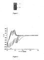
- the figure 1 represents the electrode on the surface of which the diazonium salt obtained in Example 1 will be grafted concovalently.
- This electrode has a chrome-gold stud, noted 1 in figure 1 which ensures good conduction with n-doped silicon, noted 2 in figure 1 , and makes it possible to take a point of contact in order to carry out electrografting.
- the silicon electrodes are soaked for one minute in a 1% solution of fluoridic acid (HF), then in water, and finally in isopropanol to remove the oxide layer. native and obtain a hydrogenated silicon surface.
- HF fluoridic acid
- the working electrode is immersed in a degassed acetonitrile solution comprising an electrolyte (LiClO 4 , NBu 4 PF 6 (0.1 M)) and the diazonium salt obtained in Example 1.
- a degassed acetonitrile solution comprising an electrolyte (LiClO 4 , NBu 4 PF 6 (0.1 M)) and the diazonium salt obtained in Example 1.
- the electrografting was then performed under potentiodynamic or potentiostatic conditions, at room temperature.
- the figure 2 represents the cyclic voltammetric curve obtained during the electrografting of the diazonium salt obtained in Example 1 on a n-doped silicon electrode (8 ⁇ 10 -3 / 2 ⁇ 10 -2 ⁇ .cm) when carrying out a dynamic sweep of the potential during 5 cycles between 0 and -2V as a function of Ag / Ag +.
- the voltammogram shows an irreversible wave towards -1.15 V, which corresponds to the reduction of the diazonium salt in radical which reacts with the hydrogenated silicon surface to form covalent bonds, and two waves of reduction reversible to -1.5 V and -1.75 V.
- These two reversible reduction waves are related to the reduction of bipyridine, terpyridine or phenanthroline ligands.
- the increase in intensity of the waves of reduction of the ligands of the complex by cycling between 0 and -2 V is characteristic of a modification of the surface of the electrode.
- the figure 3 represents the cyclic voltammetric curve produced on the modified electrode, ie with a film of the polymer obtained from the diazonium salt of Example 1.
- the analysis medium was salt-free. of diazonium according to the invention.
- This curve clearly shows the deposition of ruthenium complex on the surface of the silicon electrode.
- the voltammetric curves show the two reversible reduction waves characteristic of the complex with potentials identical to the initial complex.
- the polymer films grafted onto the silicon electrode have redox properties which not only allow electrons to be conveyed to the surface of the film already deposited to propagate the polymerization and thus obtain polymer films of thickness that can go up to several hundred nanometers, but also to obtain a conductive organic film on the surface of the electrode, which makes it possible to deposit, if desired, a second polymer layer of a different metal complex on the film already formed.
- Example 3 Electrografting of the Diazonium Salt Obtained in Example 1 on a Broadband Semiconductor (ZnO)
- Example 4 Charge Capture in the Polymers Obtained from the Diazonium Salt of Example 1
- the figure 4 demonstrates the capture of charges in the electrografted polymer obtained from the diazonium salt of Example 1 when the metal center of the complex grafted to the electrode has been oxidized, whether this electrode is an n-doped silicon electrode or a ZnO electrode.
- the solid-state voltammogram corresponds to the response of a film obtained by forming the diazonium salt obtained in Example 1 in potentiostatic mode, after oxidation of the metal center and the dotted line voltammogram corresponds to the response of a film obtained from the diazonium salt obtained in Example 1 in potentiostatic mode, before oxidation of the metal center.
- the film presents the two reversible reduction waves of ligands.
- the electrode is then brought to a potential of 1.2V as a function of Ag / Ag +, the electrochemical response of the deposited polymer to the electrode changes and presents an irreversible additional wave to -1.3V. This corresponds to the reduction of the charges captured during the oxidation of the metal center.
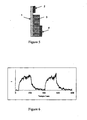
- the figure 5 represents a profile view of a device consisting of an n doped silicon electrode (14/22 ⁇ .cm), denoted 1 in figure 5 , with its chromium-gold contact, noted 2 in figure 5 , on which was formed the polymer obtained from the diazonium salt synthesized in Example 1, noted 3 in figure 5 , in potentiodynamic condition (thickness from 40 to 100 nm).
- a gold metal electrode, noted 4 in figure 5 was then deposited directly onto the film 3 by vacuum evaporation.
- the irradiation with a white light causes a current which is due to the absorption of light by the silicon semiconductor.
- the figure 6 represents the photocurrent thus caused.
- the absorption of light by the silicon semiconductor generates charges inside the semiconductor that can be extracted through the transport of holes in the previously formed redox polymer.
- the polymer serves as a solid electrolyte and avoids the photo-anodic decomposition generally obtained when using a liquid electrolyte.
- the figure 7 shows a profile view of a device consisting of an n-doped silicon electrode, denoted 1 in figure 7 , with its metallic contact in chrome-gold, noted 2 in figure 7 , on which was formed a first layer of the diazonium salt obtained in Example 1, noted 3 in figure 7 .
- Electrodes can be made on which there are several layers of metal complexes. These layers are then capable of storing charges for making memories.
- Step 1 Synthesis of [Ir (phenylpyridine) 2 (Bipyridine-phenyl-N 2 + )] PF 6 ] 2
- Step 2 Synthesis of the diazonium salt [Ir (Phenylpyridine) 2 (Bipyridine-phenyl-NH 2 )] [PF 6 ]
- Step 3 Grafting and Electrochemical Polymerization of the Diazonium Salt [[Ir (Phenylpyridine)] 2 (Bipyridine-phenyl-NH 2 )] [PF 6 ] on a platinum electrode.
- the assembly used is identical to that used in Examples 2 and 3 for the electroplating of the ruthenium comlex.
- the complex is grafted and polymerized on a metal surface which is platinum.
- the figure 8 represents the voltammetric curve obtained during the grafting of the diazonium salt of the iridium complex obtained above on a platinum electrode when conducting a dynamic sweep of the potential during 5 cycles between 0 and -1.9V according to Ag / Ag + .
- the figure 8 shows an irreversible wave towards -1,39V, which corresponds to the formation of a radical cation of the salt of diazonium and a reversible wave of reduction to -1.7V corresponding to the reduction of the complex.
- the increase in intensity of the current during the cycling between 0 and -1.9V clearly shows the formation of a deposit of the iridium complex on the surface of the electrode.
- the invention is not not limited to the electrofunctionalization of silicon surfaces of ZnO or platinum.
- the diazonium salts of the invention may make it possible to realize other devices in which the electrofunctionalization of a conductive or semiconductive surface is of interest.
Landscapes
- Chemical & Material Sciences (AREA)
- Organic Chemistry (AREA)
- Crystallography & Structural Chemistry (AREA)
- Inorganic Chemistry (AREA)
- Engineering & Computer Science (AREA)
- Materials Engineering (AREA)
- Hybrid Cells (AREA)
- Organic Low-Molecular-Weight Compounds And Preparation Thereof (AREA)
- Photovoltaic Devices (AREA)
- Graft Or Block Polymers (AREA)
- Macromolecular Compounds Obtained By Forming Nitrogen-Containing Linkages In General (AREA)
Claims (21)
- Polymerisierbare Diazoniumsalze, dadurch gekennzeichnet, dass sie Redoxeigenschaften und im sichtbaren Bereich Absorptionseigenschaften besitzen, sowie dadurch, dass sie die folgende allgemeine Formel (I) haben:
[Xx+ LnDdEm (N2 +)p] [(B-)p+x] Formel I
in der:- X für ein Übergangsmetall steht, das unter Ruthenium (Ru), Osmium (Os), Eisen (Fe), Cobalt (Co) und Iridium (Ir) ausgewählt ist,- x ein ganzzahliger Wert von einschließlich 1 bis 5 ist,- L für einen Liganden steht, der unter den Pyridin-, Bipyridin-, Terpyridin-, Phenanthrolin-, Phenylpyridingruppen und unter den Mischungen von diesen ausgewählt ist,- n ein ganzzahligerWert von einschließlich 1 bis 5 ist,- D für eine gesättigte oder ungesättigte C1-C5-Alkyl-Spacerverbindung steht,- d = 0 oder 1,- E für eine aromatische oder polyaromatische Spacerverbindung steht, die ein oder mehrere Heteroatome aufweisen kann und unter einer Benzothiophen-, Benzofuran-, Indol-, Indolin-, Carbazol-, Dehydrochinolein-, Chromon-, Julodinin-, Thiadiazol-, Triazol-, Isoxasol-, Oxazol-, Thiazol-, Isothiazol-, Imidazol-, Pyrazol-, Thiazin-, Triazin-, Pyrazin-, Pyridazin-, Pyrimidin-, Diazepin-, Oxazepin-, Benzotriazol-, Benzoaxazol-, Imidazol-, Benzimidazol-, Morpholin-, Piperidin-, Piperazin-, Azetidin-, Pyrrolidin-, Aziridingruppe, einer Phenyl-, Biphenyl-, Thiophen-, Bithiophen-, Furan-, Bifuran-, Pyridin-, Bipyridin-, Terpyridin-, Fluoren-, Fluorenongruppe oder unter Mischungen von diesen ausgewählt ist, und- B für ein Gegenion steht,- m ein ganzzahliger Wert von einschließlich 0 bis 5 ist,- p ein ganzzahliger Wert ist. - Diazoniumsalze nach Anspruch 1, dadurch gekennzeichnet, dass B für eine Chlorat-, Fosylat-, Sulfonatgruppe, ein anionisches Polymer, PF6 oder BF4 steht.
- Diazoniumsalze nach Anspruch 1, dadurch gekennzeichnet, dass B für eine PF6- oder BF4-Gruppe steht.
- Diazoniumsalze nach einem der vorherigen Ansprüche, dadurch gekennzeichnet, dass sie eine der nachfolgenden allgemeinen Formeln I-2 bis I-7 haben:


 - X unter Ruthenium (Ru), Osmium (Os), Eisen (Fe), Cobalt (Co) und Iiridium (Ir) ausgewählt ist,- Z für CH=CH, S, O, CH=N, N-H, N = N steht, und- m ein ganzzahliger Wert von einschließlich 0 bis 5 ist, und- B für BF4 oder PF6 steht.
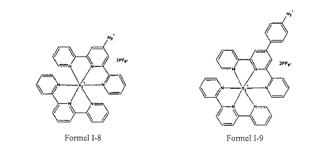
 - Diazoniumsalze nach einem der Ansprüche 1 bis 3, dadurch gekennzeichnet, dass sie eine der nachfolgenden allgemeinen Formeln I-8 bis I-12 haben:


- Diazoniumsalze nach einem der Ansprüche 1 bis 3, dadurch gekennzeichnet, dass sie eine der nachfolgenden allgemeinen Formeln I-13 bis I-14 haben:


- Diazoniumsalz nach einem der Ansprüche 1 bis 3, dadurch gekennzeichnet, dass:- X für Ruthenium (Ru) steht,- L für eine Bipyridinguppe steht,- n = 2- E für eine Bipyridin-Phenyl-Gruppe steht,- m = 1,- p = 1,- B = PF6,mit der nachfolgenden allgemeinen Formel (I-15):
[Ru(Bipyridin)2(Bipyridin-Phenyl-N2+)] [PF6]3 Formel I-15.
- Diazoniumsalz nach einem der Ansprüche 1 bis 3, dadurch gekennzeichnet, dass:- X für Iridium (Ir) steht,- L für eine Phenylpyridingruppe steht,- n = 2- E für eine Bipyridin-Phenyl-Gruppe steht,- m = 1,- p = 1,- B = PF6,mit der nachfolgenden allgemeinen Formel (I-16):
[Ir(Phenylpyridin)2(Bipypyridin-Phenyl-N2 +)][PF6]2 Formel I-16
- Verfahren für die Synthese von Diazoniumsalzen nach einem der vorherigen Ansprüche, dadurch gekennzeichnet, dass es die folgenden Schritte umfasst:- (a) Synthetisieren des gewünschen Metallkomplexes der Formel XLn, wobei alle Liganden L mindestens eine aromatische Aminfunktion aufweisen und identisch oder verschieden sein können, und- (b) Überführen der Aminfunktionen in N2 + unter Verwendung von NOBF4.
- Verfahren zur Ausbildung einer Monoschicht von Polymer, das Redoxeigenschaften und im sichtbaren Bereich Absorptionseigenschaften besitzt, auf einer leitenden oder halbleitenden Oberfläche, dadurch gekennzeichnet, dass es umfasst: einen Schritt des elektrochemischen Aufpfropfens eines Diazoniumsalzes nach einem der Ansprüche 1 bis 8, und einen Schritt des Polymerisierens dieses Diazoniumsalzes, um einen Polymerfilm mit der gewünschten Dicke zu erhalten.
- Verfahren zur Ausbildung von Mehrfachschichten von Polymeren, die Redoxeigenschaften und im sichtbaren Bereich Absorptionseigenschaften besitzen, auf einer leitenden oder halbleitenden Oberfläche, dadurch gekennzeichnet, dass es die folgenden Schritte umfasst:(a) elektrochemisches Aufpfropfen eines polymerisierbaren Diazoniumsalzes nach einem der Ansprüche 1 bis 8 auf die genannte Oberfläche,(b) Polymerisieren dieses Diazoniumsalzes zum Ausbilden eines ersten Polymerfilms mit der gewünschten Dicke,(c) mindestens einen Schritt des Aufpfropfens eines polymerisierbaren Diazoniumsalzes nach einem der Ansprüche 1 bis 8 auf den in Schritt (a) erhaltenen Film, wobei dieses Diazoniumsalz mit dem in Schritt (a) verwendeten Diazoniumsalz identisch oder davon verschieden ist, und(d) Polymerisieren dieses Diazoniumsalzes zum Ausbilden eines zweiten Polymerfilms mit der gewünschten Dicke.
- Verfahren nach Anspruch 10 oder 11, dadurch gekennzeichnet, dass die halbleitende Oberfläche eine Silicium- oder Platinoberfläche ist.
- Verfahren nach Anspruch 10 oder 11, dadurch gekennzeichnet, dass die halbleitende Oberfläche die Oberfläche eines Kohlenstoff-Nanoröhrchens ist.
- Verfahren nach Anspruch 10 oder 11, dadurch gekennzeichnet, dass die halbleitende Oberfläche die Oberfläche eines Nanopartikels von Titanoxid (TiO2), Zinnoxid (SnO2), Zinkoxid (ZnO) oder Zirconium(IV)-oxid (ZrO2) ist.
- Substrat, dadurch gekennzeichnet, dass es mindestens eine Oberfläche aufweist, die mindestens eine Schicht aus Polymer aufweist, welches aus einem polymerisierbaren Diazoniumsalz nach einem der Ansprüche 1 bis 8 erhalten wurde.
- Vorrichtung, dadurch gekennzeichnet, dass sie mindestens ein Substrat nach Anspruch 15 aufweist.
- Photovoltaische Zelle, insbesondere vom Grätzel-Typ, dadurch gekennzeichnet, dass sie mindestens ein Substrat nach Anspruch 15 aufweist.
- Informationsspeicherzelle mit Redoxaktivität, dadurch gekennzeichnet, dass sie mindestens ein Substrat nach Anspruch 15 aufweist.
- Breitband-Halbleitervorrichtung, dadurch gekennzeichnet, dass sie mindestens ein Substrat nach Anspruch 15 aufweist.
- Photovoltaische Zelle vom Grätzel-Typ, dadurch gekennzeichnet, dass sie einen festen Elektrolyten aufweist, der mindestens ein polymerisierbares Diazoniumsalz nach einem der Ansprüche 1 bis 8 aufweist.
- Fester leitender Elektrolyt, dadurch gekennzeichnet, dass er mindestens ein Diazoniumsalz nach einem der Ansprüche 1 bis 8 aufweist.
Applications Claiming Priority (1)
| Application Number | Priority Date | Filing Date | Title |
|---|---|---|---|
| FR0606906A FR2904319B1 (fr) | 2006-07-27 | 2006-07-27 | Sels de diazonium polymerisables, procede de fabrication et utilisations de ceux-ci |
Publications (2)
| Publication Number | Publication Date |
|---|---|
| EP1921084A1 EP1921084A1 (de) | 2008-05-14 |
| EP1921084B1 true EP1921084B1 (de) | 2011-03-02 |
Family
ID=37813799
Family Applications (1)
| Application Number | Title | Priority Date | Filing Date |
|---|---|---|---|
| EP07290888A Active EP1921084B1 (de) | 2006-07-27 | 2007-07-16 | Polmerisierbare Diazoniumsalze, Verfahren zu deren Herstellung und deren Verwendung |
Country Status (5)
| Country | Link |
|---|---|
| US (2) | US7812139B2 (de) |
| EP (1) | EP1921084B1 (de) |
| AT (1) | ATE500260T1 (de) |
| DE (1) | DE602007012808D1 (de) |
| FR (1) | FR2904319B1 (de) |
Families Citing this family (9)
| Publication number | Priority date | Publication date | Assignee | Title |
|---|---|---|---|---|
| US7176146B2 (en) * | 2002-02-01 | 2007-02-13 | William Marsh Rice University | Method of making a molecule-surface interface |
| US8362559B2 (en) * | 2002-02-01 | 2013-01-29 | William Marsh Rice University | Hybrid molecular electronic devices containing molecule-functionalized surfaces for switching, memory, and sensor applications and methods for fabricating same |
| FR2892325B1 (fr) * | 2005-10-26 | 2008-01-18 | Alchimer Sa | Procede de modification de surfaces isolantes, semi-conductrices ou metalliques, et produits tels qu'obtenus |
| US7771115B2 (en) * | 2007-08-16 | 2010-08-10 | Micron Technology, Inc. | Temperature sensor circuit, device, system, and method |
| US20090048414A1 (en) * | 2007-08-16 | 2009-02-19 | Uchicago Argonne, Llc | Magnetic coupling through strong hydrogen bonds |
| FR2929618B1 (fr) * | 2008-04-03 | 2011-03-18 | Commissariat Energie Atomique | Procede pour assembler deux surfaces ou une surface avec une molecule d'interet |
| KR101634753B1 (ko) * | 2008-11-28 | 2016-06-30 | 삼성전자주식회사 | 탄소나노튜브 엔 도핑 물질 및 이를 이용한 엔 도핑 방법 |
| FR2964102B1 (fr) | 2010-09-01 | 2013-03-29 | Commissariat Energie Atomique | Utilisation de sels de diazonium pour la formation de couches epaisses sur au moins une surface d'un substrat |
| CN108922785B (zh) * | 2018-09-08 | 2020-04-28 | 温州涌润信息科技有限公司 | 一种染料敏化太阳能电池对电极材料的制备方法 |
Family Cites Families (3)
| Publication number | Priority date | Publication date | Assignee | Title |
|---|---|---|---|---|
| EP1033731B1 (de) * | 1999-03-01 | 2006-07-05 | Fuji Photo Film Co., Ltd. | Photoelektrochemische Zelle mit einem Elektrolyten aus Flüssigkristallverbindungen |
| US20060005877A1 (en) * | 2004-07-06 | 2006-01-12 | General Electric Company | Passivated, dye-sensitized oxide semiconductor electrode, solar cell using same, and method |
| US7122171B2 (en) * | 2004-12-02 | 2006-10-17 | Virginia Tech Intellectual Properties, Inc. | Supramolecular complexes as photocatylysts for the production of hydrogen from water |
-
2006
- 2006-07-27 FR FR0606906A patent/FR2904319B1/fr not_active Expired - Fee Related
-
2007
- 2007-07-16 EP EP07290888A patent/EP1921084B1/de active Active
- 2007-07-16 AT AT07290888T patent/ATE500260T1/de not_active IP Right Cessation
- 2007-07-16 DE DE602007012808T patent/DE602007012808D1/de active Active
- 2007-07-24 US US11/782,218 patent/US7812139B2/en not_active Expired - Fee Related
-
2010
- 2010-03-30 US US12/750,424 patent/US8389696B2/en not_active Expired - Fee Related
Also Published As
| Publication number | Publication date |
|---|---|
| US20100184932A1 (en) | 2010-07-22 |
| FR2904319B1 (fr) | 2009-10-30 |
| FR2904319A1 (fr) | 2008-02-01 |
| US8389696B2 (en) | 2013-03-05 |
| DE602007012808D1 (de) | 2011-04-14 |
| ATE500260T1 (de) | 2011-03-15 |
| EP1921084A1 (de) | 2008-05-14 |
| US7812139B2 (en) | 2010-10-12 |
| US20080236666A1 (en) | 2008-10-02 |
Similar Documents
| Publication | Publication Date | Title |
|---|---|---|
| EP1921084B1 (de) | Polmerisierbare Diazoniumsalze, Verfahren zu deren Herstellung und deren Verwendung | |
| Magomedov et al. | Pyridination of hole transporting material in perovskite solar cells questions the long-term stability | |
| Yanagida et al. | Polythiophene-sensitized TiO2 solar cells | |
| Wang et al. | Facile synthesis and high performance of a new carbazole-based hole-transporting material for hybrid perovskite solar cells | |
| Senadeera et al. | Deposition of polyaniline via molecular self-assembly on TiO2 and its uses as a sensitiser in solid-state solar cells | |
| CN102138249B (zh) | 光电器件 | |
| Sharmoukh et al. | Molecular engineering of D–D− π–A-based organic sensitizers for enhanced dye-sensitized solar cell performance | |
| Lin et al. | Donor–acceptor–donor type cyclopenta [2, 1-b; 3, 4-b′] dithiophene derivatives as a new class of hole transporting materials for highly efficient and stable perovskite solar cells | |
| US20090293951A1 (en) | Dye for dye-sensitized solar cell and dye-sensitized solar cell including the same | |
| Mao et al. | Design of Bodipy based organic dyes for high-efficient dye-sensitized solar cells employing double electron acceptors | |
| JP6737798B2 (ja) | 光電子及び光電気化学デバイスのための小分子ホール輸送材料 | |
| Tomkeviciene et al. | Diphenylamino-substituted derivatives of 9-phenylcarbazole as glass-forming hole-transporting materials for solid state dye sensitized solar cells | |
| JP2009269987A (ja) | 新規化合物、光電変換素子及び太陽電池 | |
| Ionescu et al. | Electropolymerized highly photoconductive thin films of cyclopalladated and cycloplatinated complexes | |
| Hilmi et al. | Universal low-temperature MWCNT-COOH-based counter electrode and a new thiolate/disulfide electrolyte system for dye-sensitized solar cells | |
| Ooyama et al. | Photovoltaic performances of type-II dye-sensitized solar cells based on catechol dye sensitizers: retardation of back-electron transfer by PET (photo-induced electron transfer) | |
| Onozawa-Komatsuzaki et al. | Highly efficient dopant-free cyano-substituted spiro-type hole-transporting materials for perovskite solar cells | |
| Choi et al. | Efficient Hole‐Transporting Materials with Triazole Core for High‐Efficiency Perovskite Solar Cells | |
| Raymakers et al. | Functionalization of boron-doped diamond with a push–pull chromophore via Sonogashira and CuAAC chemistry | |
| FR3011548A1 (fr) | Compose organique photoactif | |
| Akula et al. | Novel thieno-imidazole salt-based hole transport material for dopant-free, efficient inverted perovskite solar cell applications | |
| Ketavath et al. | Unadorned molecular engineering of phenoxazine-core-based hole-transport materials for sustainable perovskite solar cells | |
| WO2004030029A2 (en) | Conducting polymer devices for inter-converting light and electricity | |
| EP2763798B1 (de) | Verfahren zur funktionalisierung eines festen substrats ohne gold durch spezifische chemische verbindungen | |
| Sadeghi et al. | Design and development of a low-cost imidazole-based hole transporting material for perovskite solar cells |
Legal Events
| Date | Code | Title | Description |
|---|---|---|---|
| PUAI | Public reference made under article 153(3) epc to a published international application that has entered the european phase |
Free format text: ORIGINAL CODE: 0009012 |
|
| AK | Designated contracting states |
Kind code of ref document: A1 Designated state(s): AT BE BG CH CY CZ DE DK EE ES FI FR GB GR HU IE IS IT LI LT LU LV MC MT NL PL PT RO SE SI SK TR |
|
| AX | Request for extension of the european patent |
Extension state: AL BA HR MK RS |
|
| 17P | Request for examination filed |
Effective date: 20081027 |
|
| 17Q | First examination report despatched |
Effective date: 20081217 |
|
| AKX | Designation fees paid |
Designated state(s): AT BE BG CH CY CZ DE DK EE ES FI FR GB GR HU IE IS IT LI LT LU LV MC MT NL PL PT RO SE SI SK TR |
|
| AXX | Extension fees paid |
Extension state: MK Payment date: 20081027 Extension state: BA Payment date: 20081027 Extension state: AL Payment date: 20081027 Extension state: HR Payment date: 20081027 Extension state: RS Payment date: 20081027 |
|
| RAP1 | Party data changed (applicant data changed or rights of an application transferred) |
Owner name: COMMISSARIAT A L'ENERGIE ATOMIQUE ET AUX ENERGIES |
|
| GRAP | Despatch of communication of intention to grant a patent |
Free format text: ORIGINAL CODE: EPIDOSNIGR1 |
|
| GRAS | Grant fee paid |
Free format text: ORIGINAL CODE: EPIDOSNIGR3 |
|
| GRAA | (expected) grant |
Free format text: ORIGINAL CODE: 0009210 |
|
| AK | Designated contracting states |
Kind code of ref document: B1 Designated state(s): AT BE BG CH CY CZ DE DK EE ES FI FR GB GR HU IE IS IT LI LT LU LV MC MT NL PL PT RO SE SI SK TR |
|
| AX | Request for extension of the european patent |
Extension state: AL BA HR MK RS |
|
| REG | Reference to a national code |
Ref country code: GB Ref legal event code: FG4D Free format text: NOT ENGLISH |
|
| REG | Reference to a national code |
Ref country code: CH Ref legal event code: EP |
|
| REG | Reference to a national code |
Ref country code: IE Ref legal event code: FG4D Free format text: LANGUAGE OF EP DOCUMENT: FRENCH |
|
| REF | Corresponds to: |
Ref document number: 602007012808 Country of ref document: DE Date of ref document: 20110414 Kind code of ref document: P |
|
| REG | Reference to a national code |
Ref country code: DE Ref legal event code: R096 Ref document number: 602007012808 Country of ref document: DE Effective date: 20110414 |
|
| REG | Reference to a national code |
Ref country code: NL Ref legal event code: VDEP Effective date: 20110302 |
|
| PG25 | Lapsed in a contracting state [announced via postgrant information from national office to epo] |
Ref country code: LV Free format text: LAPSE BECAUSE OF FAILURE TO SUBMIT A TRANSLATION OF THE DESCRIPTION OR TO PAY THE FEE WITHIN THE PRESCRIBED TIME-LIMIT Effective date: 20110302 Ref country code: SE Free format text: LAPSE BECAUSE OF FAILURE TO SUBMIT A TRANSLATION OF THE DESCRIPTION OR TO PAY THE FEE WITHIN THE PRESCRIBED TIME-LIMIT Effective date: 20110302 Ref country code: ES Free format text: LAPSE BECAUSE OF FAILURE TO SUBMIT A TRANSLATION OF THE DESCRIPTION OR TO PAY THE FEE WITHIN THE PRESCRIBED TIME-LIMIT Effective date: 20110613 Ref country code: GR Free format text: LAPSE BECAUSE OF FAILURE TO SUBMIT A TRANSLATION OF THE DESCRIPTION OR TO PAY THE FEE WITHIN THE PRESCRIBED TIME-LIMIT Effective date: 20110603 Ref country code: LT Free format text: LAPSE BECAUSE OF FAILURE TO SUBMIT A TRANSLATION OF THE DESCRIPTION OR TO PAY THE FEE WITHIN THE PRESCRIBED TIME-LIMIT Effective date: 20110302 |
|
| LTIE | Lt: invalidation of european patent or patent extension |
Effective date: 20110302 |
|
| PG25 | Lapsed in a contracting state [announced via postgrant information from national office to epo] |
Ref country code: CY Free format text: LAPSE BECAUSE OF FAILURE TO SUBMIT A TRANSLATION OF THE DESCRIPTION OR TO PAY THE FEE WITHIN THE PRESCRIBED TIME-LIMIT Effective date: 20110302 Ref country code: AT Free format text: LAPSE BECAUSE OF FAILURE TO SUBMIT A TRANSLATION OF THE DESCRIPTION OR TO PAY THE FEE WITHIN THE PRESCRIBED TIME-LIMIT Effective date: 20110302 Ref country code: NL Free format text: LAPSE BECAUSE OF FAILURE TO SUBMIT A TRANSLATION OF THE DESCRIPTION OR TO PAY THE FEE WITHIN THE PRESCRIBED TIME-LIMIT Effective date: 20110302 Ref country code: FI Free format text: LAPSE BECAUSE OF FAILURE TO SUBMIT A TRANSLATION OF THE DESCRIPTION OR TO PAY THE FEE WITHIN THE PRESCRIBED TIME-LIMIT Effective date: 20110302 Ref country code: SI Free format text: LAPSE BECAUSE OF FAILURE TO SUBMIT A TRANSLATION OF THE DESCRIPTION OR TO PAY THE FEE WITHIN THE PRESCRIBED TIME-LIMIT Effective date: 20110302 Ref country code: BG Free format text: LAPSE BECAUSE OF FAILURE TO SUBMIT A TRANSLATION OF THE DESCRIPTION OR TO PAY THE FEE WITHIN THE PRESCRIBED TIME-LIMIT Effective date: 20110602 |
|
| REG | Reference to a national code |
Ref country code: IE Ref legal event code: FD4D |
|
| PG25 | Lapsed in a contracting state [announced via postgrant information from national office to epo] |
Ref country code: EE Free format text: LAPSE BECAUSE OF FAILURE TO SUBMIT A TRANSLATION OF THE DESCRIPTION OR TO PAY THE FEE WITHIN THE PRESCRIBED TIME-LIMIT Effective date: 20110302 Ref country code: IE Free format text: LAPSE BECAUSE OF FAILURE TO SUBMIT A TRANSLATION OF THE DESCRIPTION OR TO PAY THE FEE WITHIN THE PRESCRIBED TIME-LIMIT Effective date: 20110302 Ref country code: PT Free format text: LAPSE BECAUSE OF FAILURE TO SUBMIT A TRANSLATION OF THE DESCRIPTION OR TO PAY THE FEE WITHIN THE PRESCRIBED TIME-LIMIT Effective date: 20110704 |
|
| PG25 | Lapsed in a contracting state [announced via postgrant information from national office to epo] |
Ref country code: SK Free format text: LAPSE BECAUSE OF FAILURE TO SUBMIT A TRANSLATION OF THE DESCRIPTION OR TO PAY THE FEE WITHIN THE PRESCRIBED TIME-LIMIT Effective date: 20110302 Ref country code: CZ Free format text: LAPSE BECAUSE OF FAILURE TO SUBMIT A TRANSLATION OF THE DESCRIPTION OR TO PAY THE FEE WITHIN THE PRESCRIBED TIME-LIMIT Effective date: 20110302 Ref country code: RO Free format text: LAPSE BECAUSE OF FAILURE TO SUBMIT A TRANSLATION OF THE DESCRIPTION OR TO PAY THE FEE WITHIN THE PRESCRIBED TIME-LIMIT Effective date: 20110302 Ref country code: IS Free format text: LAPSE BECAUSE OF FAILURE TO SUBMIT A TRANSLATION OF THE DESCRIPTION OR TO PAY THE FEE WITHIN THE PRESCRIBED TIME-LIMIT Effective date: 20110702 |
|
| PG25 | Lapsed in a contracting state [announced via postgrant information from national office to epo] |
Ref country code: MT Free format text: LAPSE BECAUSE OF FAILURE TO SUBMIT A TRANSLATION OF THE DESCRIPTION OR TO PAY THE FEE WITHIN THE PRESCRIBED TIME-LIMIT Effective date: 20110302 |
|
| PLBE | No opposition filed within time limit |
Free format text: ORIGINAL CODE: 0009261 |
|
| STAA | Information on the status of an ep patent application or granted ep patent |
Free format text: STATUS: NO OPPOSITION FILED WITHIN TIME LIMIT |
|
| BERE | Be: lapsed |
Owner name: COMMISSARIAT A L'ENERGIE ATOMIQUE ET AUX ENERGIES Effective date: 20110731 |
|
| 26N | No opposition filed |
Effective date: 20111205 |
|
| PG25 | Lapsed in a contracting state [announced via postgrant information from national office to epo] |
Ref country code: PL Free format text: LAPSE BECAUSE OF FAILURE TO SUBMIT A TRANSLATION OF THE DESCRIPTION OR TO PAY THE FEE WITHIN THE PRESCRIBED TIME-LIMIT Effective date: 20110302 Ref country code: MC Free format text: LAPSE BECAUSE OF NON-PAYMENT OF DUE FEES Effective date: 20110731 Ref country code: DK Free format text: LAPSE BECAUSE OF FAILURE TO SUBMIT A TRANSLATION OF THE DESCRIPTION OR TO PAY THE FEE WITHIN THE PRESCRIBED TIME-LIMIT Effective date: 20110302 |
|
| REG | Reference to a national code |
Ref country code: CH Ref legal event code: PL |
|
| REG | Reference to a national code |
Ref country code: DE Ref legal event code: R097 Ref document number: 602007012808 Country of ref document: DE Effective date: 20111205 |
|
| PG25 | Lapsed in a contracting state [announced via postgrant information from national office to epo] |
Ref country code: CH Free format text: LAPSE BECAUSE OF NON-PAYMENT OF DUE FEES Effective date: 20110731 Ref country code: LI Free format text: LAPSE BECAUSE OF NON-PAYMENT OF DUE FEES Effective date: 20110731 Ref country code: BE Free format text: LAPSE BECAUSE OF NON-PAYMENT OF DUE FEES Effective date: 20110731 |
|
| PG25 | Lapsed in a contracting state [announced via postgrant information from national office to epo] |
Ref country code: LU Free format text: LAPSE BECAUSE OF NON-PAYMENT OF DUE FEES Effective date: 20110716 |
|
| PG25 | Lapsed in a contracting state [announced via postgrant information from national office to epo] |
Ref country code: TR Free format text: LAPSE BECAUSE OF FAILURE TO SUBMIT A TRANSLATION OF THE DESCRIPTION OR TO PAY THE FEE WITHIN THE PRESCRIBED TIME-LIMIT Effective date: 20110302 |
|
| PG25 | Lapsed in a contracting state [announced via postgrant information from national office to epo] |
Ref country code: HU Free format text: LAPSE BECAUSE OF FAILURE TO SUBMIT A TRANSLATION OF THE DESCRIPTION OR TO PAY THE FEE WITHIN THE PRESCRIBED TIME-LIMIT Effective date: 20110302 |
|
| PGFP | Annual fee paid to national office [announced via postgrant information from national office to epo] |
Ref country code: DE Payment date: 20130709 Year of fee payment: 7 |
|
| PGFP | Annual fee paid to national office [announced via postgrant information from national office to epo] |
Ref country code: GB Payment date: 20130719 Year of fee payment: 7 Ref country code: FR Payment date: 20130731 Year of fee payment: 7 |
|
| PGFP | Annual fee paid to national office [announced via postgrant information from national office to epo] |
Ref country code: IT Payment date: 20130711 Year of fee payment: 7 |
|
| REG | Reference to a national code |
Ref country code: DE Ref legal event code: R119 Ref document number: 602007012808 Country of ref document: DE |
|
| GBPC | Gb: european patent ceased through non-payment of renewal fee |
Effective date: 20140716 |
|
| REG | Reference to a national code |
Ref country code: DE Ref legal event code: R119 Ref document number: 602007012808 Country of ref document: DE Effective date: 20150203 |
|
| REG | Reference to a national code |
Ref country code: FR Ref legal event code: ST Effective date: 20150331 |
|
| PG25 | Lapsed in a contracting state [announced via postgrant information from national office to epo] |
Ref country code: DE Free format text: LAPSE BECAUSE OF NON-PAYMENT OF DUE FEES Effective date: 20150203 Ref country code: IT Free format text: LAPSE BECAUSE OF NON-PAYMENT OF DUE FEES Effective date: 20140716 |
|
| PG25 | Lapsed in a contracting state [announced via postgrant information from national office to epo] |
Ref country code: GB Free format text: LAPSE BECAUSE OF NON-PAYMENT OF DUE FEES Effective date: 20140716 Ref country code: FR Free format text: LAPSE BECAUSE OF NON-PAYMENT OF DUE FEES Effective date: 20140731 |