EP1921494A2 - Tragbare Anzeigevorrichtung - Google Patents
Tragbare Anzeigevorrichtung Download PDFInfo
- Publication number
- EP1921494A2 EP1921494A2 EP07254419A EP07254419A EP1921494A2 EP 1921494 A2 EP1921494 A2 EP 1921494A2 EP 07254419 A EP07254419 A EP 07254419A EP 07254419 A EP07254419 A EP 07254419A EP 1921494 A2 EP1921494 A2 EP 1921494A2
- Authority
- EP
- European Patent Office
- Prior art keywords
- light
- light source
- liquid crystal
- display panel
- crystal display
- Prior art date
- Legal status (The legal status is an assumption and is not a legal conclusion. Google has not performed a legal analysis and makes no representation as to the accuracy of the status listed.)
- Ceased
Links
Images


Classifications
-
- G—PHYSICS
- G02—OPTICS
- G02F—OPTICAL DEVICES OR ARRANGEMENTS FOR THE CONTROL OF LIGHT BY MODIFICATION OF THE OPTICAL PROPERTIES OF THE MEDIA OF THE ELEMENTS INVOLVED THEREIN; NON-LINEAR OPTICS; FREQUENCY-CHANGING OF LIGHT; OPTICAL LOGIC ELEMENTS; OPTICAL ANALOGUE/DIGITAL CONVERTERS
- G02F1/00—Devices or arrangements for the control of the intensity, colour, phase, polarisation or direction of light arriving from an independent light source, e.g. switching, gating or modulating; Non-linear optics
- G02F1/01—Devices or arrangements for the control of the intensity, colour, phase, polarisation or direction of light arriving from an independent light source, e.g. switching, gating or modulating; Non-linear optics for the control of the intensity, phase, polarisation or colour
- G02F1/13—Devices or arrangements for the control of the intensity, colour, phase, polarisation or direction of light arriving from an independent light source, e.g. switching, gating or modulating; Non-linear optics for the control of the intensity, phase, polarisation or colour based on liquid crystals, e.g. single liquid crystal display cells
- G02F1/133—Constructional arrangements; Operation of liquid crystal cells; Circuit arrangements
- G02F1/1333—Constructional arrangements; Manufacturing methods
-
- G—PHYSICS
- G02—OPTICS
- G02F—OPTICAL DEVICES OR ARRANGEMENTS FOR THE CONTROL OF LIGHT BY MODIFICATION OF THE OPTICAL PROPERTIES OF THE MEDIA OF THE ELEMENTS INVOLVED THEREIN; NON-LINEAR OPTICS; FREQUENCY-CHANGING OF LIGHT; OPTICAL LOGIC ELEMENTS; OPTICAL ANALOGUE/DIGITAL CONVERTERS
- G02F1/00—Devices or arrangements for the control of the intensity, colour, phase, polarisation or direction of light arriving from an independent light source, e.g. switching, gating or modulating; Non-linear optics
- G02F1/01—Devices or arrangements for the control of the intensity, colour, phase, polarisation or direction of light arriving from an independent light source, e.g. switching, gating or modulating; Non-linear optics for the control of the intensity, phase, polarisation or colour
- G02F1/13—Devices or arrangements for the control of the intensity, colour, phase, polarisation or direction of light arriving from an independent light source, e.g. switching, gating or modulating; Non-linear optics for the control of the intensity, phase, polarisation or colour based on liquid crystals, e.g. single liquid crystal display cells
- G02F1/133—Constructional arrangements; Operation of liquid crystal cells; Circuit arrangements
- G02F1/1333—Constructional arrangements; Manufacturing methods
- G02F1/133382—Heating or cooling of liquid crystal cells other than for activation, e.g. circuits or arrangements for temperature control, stabilisation or uniform distribution over the cell
-
- G—PHYSICS
- G02—OPTICS
- G02B—OPTICAL ELEMENTS, SYSTEMS OR APPARATUS
- G02B6/00—Light guides; Structural details of arrangements comprising light guides and other optical elements, e.g. couplings
- G02B6/0001—Light guides; Structural details of arrangements comprising light guides and other optical elements, e.g. couplings specially adapted for lighting devices or systems
- G02B6/0011—Light guides; Structural details of arrangements comprising light guides and other optical elements, e.g. couplings specially adapted for lighting devices or systems the light guides being planar or of plate-like form
- G02B6/0081—Mechanical or electrical aspects of the light guide and light source in the lighting device peculiar to the adaptation to planar light guides, e.g. concerning packaging
- G02B6/0085—Means for removing heat created by the light source from the package
-
- G—PHYSICS
- G02—OPTICS
- G02B—OPTICAL ELEMENTS, SYSTEMS OR APPARATUS
- G02B6/00—Light guides; Structural details of arrangements comprising light guides and other optical elements, e.g. couplings
- G02B6/0001—Light guides; Structural details of arrangements comprising light guides and other optical elements, e.g. couplings specially adapted for lighting devices or systems
- G02B6/0011—Light guides; Structural details of arrangements comprising light guides and other optical elements, e.g. couplings specially adapted for lighting devices or systems the light guides being planar or of plate-like form
- G02B6/0081—Mechanical or electrical aspects of the light guide and light source in the lighting device peculiar to the adaptation to planar light guides, e.g. concerning packaging
- G02B6/0086—Positioning aspects
- G02B6/009—Positioning aspects of the light source in the package
-
- G—PHYSICS
- G02—OPTICS
- G02F—OPTICAL DEVICES OR ARRANGEMENTS FOR THE CONTROL OF LIGHT BY MODIFICATION OF THE OPTICAL PROPERTIES OF THE MEDIA OF THE ELEMENTS INVOLVED THEREIN; NON-LINEAR OPTICS; FREQUENCY-CHANGING OF LIGHT; OPTICAL LOGIC ELEMENTS; OPTICAL ANALOGUE/DIGITAL CONVERTERS
- G02F1/00—Devices or arrangements for the control of the intensity, colour, phase, polarisation or direction of light arriving from an independent light source, e.g. switching, gating or modulating; Non-linear optics
- G02F1/01—Devices or arrangements for the control of the intensity, colour, phase, polarisation or direction of light arriving from an independent light source, e.g. switching, gating or modulating; Non-linear optics for the control of the intensity, phase, polarisation or colour
- G02F1/13—Devices or arrangements for the control of the intensity, colour, phase, polarisation or direction of light arriving from an independent light source, e.g. switching, gating or modulating; Non-linear optics for the control of the intensity, phase, polarisation or colour based on liquid crystals, e.g. single liquid crystal display cells
- G02F1/133—Constructional arrangements; Operation of liquid crystal cells; Circuit arrangements
- G02F1/1333—Constructional arrangements; Manufacturing methods
- G02F1/133308—Support structures for LCD panels, e.g. frames or bezels
-
- G—PHYSICS
- G02—OPTICS
- G02F—OPTICAL DEVICES OR ARRANGEMENTS FOR THE CONTROL OF LIGHT BY MODIFICATION OF THE OPTICAL PROPERTIES OF THE MEDIA OF THE ELEMENTS INVOLVED THEREIN; NON-LINEAR OPTICS; FREQUENCY-CHANGING OF LIGHT; OPTICAL LOGIC ELEMENTS; OPTICAL ANALOGUE/DIGITAL CONVERTERS
- G02F1/00—Devices or arrangements for the control of the intensity, colour, phase, polarisation or direction of light arriving from an independent light source, e.g. switching, gating or modulating; Non-linear optics
- G02F1/01—Devices or arrangements for the control of the intensity, colour, phase, polarisation or direction of light arriving from an independent light source, e.g. switching, gating or modulating; Non-linear optics for the control of the intensity, phase, polarisation or colour
- G02F1/13—Devices or arrangements for the control of the intensity, colour, phase, polarisation or direction of light arriving from an independent light source, e.g. switching, gating or modulating; Non-linear optics for the control of the intensity, phase, polarisation or colour based on liquid crystals, e.g. single liquid crystal display cells
- G02F1/133—Constructional arrangements; Operation of liquid crystal cells; Circuit arrangements
- G02F1/1333—Constructional arrangements; Manufacturing methods
- G02F1/1335—Structural association of cells with optical devices, e.g. polarisers or reflectors
- G02F1/1336—Illuminating devices
- G02F1/133615—Edge-illuminating devices, i.e. illuminating from the side
-
- G—PHYSICS
- G02—OPTICS
- G02F—OPTICAL DEVICES OR ARRANGEMENTS FOR THE CONTROL OF LIGHT BY MODIFICATION OF THE OPTICAL PROPERTIES OF THE MEDIA OF THE ELEMENTS INVOLVED THEREIN; NON-LINEAR OPTICS; FREQUENCY-CHANGING OF LIGHT; OPTICAL LOGIC ELEMENTS; OPTICAL ANALOGUE/DIGITAL CONVERTERS
- G02F1/00—Devices or arrangements for the control of the intensity, colour, phase, polarisation or direction of light arriving from an independent light source, e.g. switching, gating or modulating; Non-linear optics
- G02F1/01—Devices or arrangements for the control of the intensity, colour, phase, polarisation or direction of light arriving from an independent light source, e.g. switching, gating or modulating; Non-linear optics for the control of the intensity, phase, polarisation or colour
- G02F1/13—Devices or arrangements for the control of the intensity, colour, phase, polarisation or direction of light arriving from an independent light source, e.g. switching, gating or modulating; Non-linear optics for the control of the intensity, phase, polarisation or colour based on liquid crystals, e.g. single liquid crystal display cells
- G02F1/133—Constructional arrangements; Operation of liquid crystal cells; Circuit arrangements
- G02F1/1333—Constructional arrangements; Manufacturing methods
- G02F1/133308—Support structures for LCD panels, e.g. frames or bezels
- G02F1/133317—Intermediate frames, e.g. between backlight housing and front frame
-
- G—PHYSICS
- G02—OPTICS
- G02F—OPTICAL DEVICES OR ARRANGEMENTS FOR THE CONTROL OF LIGHT BY MODIFICATION OF THE OPTICAL PROPERTIES OF THE MEDIA OF THE ELEMENTS INVOLVED THEREIN; NON-LINEAR OPTICS; FREQUENCY-CHANGING OF LIGHT; OPTICAL LOGIC ELEMENTS; OPTICAL ANALOGUE/DIGITAL CONVERTERS
- G02F1/00—Devices or arrangements for the control of the intensity, colour, phase, polarisation or direction of light arriving from an independent light source, e.g. switching, gating or modulating; Non-linear optics
- G02F1/01—Devices or arrangements for the control of the intensity, colour, phase, polarisation or direction of light arriving from an independent light source, e.g. switching, gating or modulating; Non-linear optics for the control of the intensity, phase, polarisation or colour
- G02F1/13—Devices or arrangements for the control of the intensity, colour, phase, polarisation or direction of light arriving from an independent light source, e.g. switching, gating or modulating; Non-linear optics for the control of the intensity, phase, polarisation or colour based on liquid crystals, e.g. single liquid crystal display cells
- G02F1/133—Constructional arrangements; Operation of liquid crystal cells; Circuit arrangements
- G02F1/1333—Constructional arrangements; Manufacturing methods
- G02F1/1335—Structural association of cells with optical devices, e.g. polarisers or reflectors
- G02F1/1336—Illuminating devices
- G02F1/133628—Illuminating devices with cooling means
-
- G—PHYSICS
- G02—OPTICS
- G02F—OPTICAL DEVICES OR ARRANGEMENTS FOR THE CONTROL OF LIGHT BY MODIFICATION OF THE OPTICAL PROPERTIES OF THE MEDIA OF THE ELEMENTS INVOLVED THEREIN; NON-LINEAR OPTICS; FREQUENCY-CHANGING OF LIGHT; OPTICAL LOGIC ELEMENTS; OPTICAL ANALOGUE/DIGITAL CONVERTERS
- G02F2201/00—Constructional arrangements not provided for in groups G02F1/00 - G02F7/00
- G02F2201/36—Airflow channels, e.g. constructional arrangements facilitating the flow of air
Definitions
- the present invention relates to a portable display device having a liquid crystal display device, and more particularly to a portable display device capable of preventing the ambient temperature of a light source provided in a liquid crystal display device being raised.
- FPD flat panel display
- LCD liquid crystal display
- FED field emission display
- PDP plasma display panel
- LED light emitting display
- a liquid crystal display device which has advantages of a miniature size, light weight and low power, has been spotlighted as a replacement able to overcome the disadvantage of a conventional cathode ray tube, and it has been currently mounted on portable apparatus such as a cellular phone and a portable digital assistor (PDA), as well as small and large products such as a monitor and TV.
- portable apparatus such as a cellular phone and a portable digital assistor (PDA)
- PDA portable digital assistor
- a contemporary portable display device is construed with a liquid crystal display panel, a backlight assembly, a bottom chassis, first and second printed circuit boards and a light-emitting display panel.
- the liquid crystal display panel which displays a video image is constructed with a first substrate, a second substrate and a liquid crystal injected between the first and second substrates.
- An integrated circuit is inserted to one side of the second substrate.
- the backlight assembly is constructed with light-emitting diodes, a light-emitting diode substrate, a light guide plate, a reflecting plate, optical sheets and a mold frame.
- the light-emitting diodes function as a light source for the liquid crystal display device and are mounted on the light-emitting diode substrate.
- the light-emitting diode substrate supplies the driving signals to the light-emitting diodes.
- At least one circuit component is mounted on the light emitting diode substrate.
- the light guide plate supplies the light generated from the light-emitting diodes to the liquid crystal display panel. Therefore, the light emitting diodes are disposed immediately adjacent to the light guide plate.
- the liquid crystal display panel In the mold frame, the liquid crystal display panel, the light-emitting diode substrate constructed with the light-emitting diode which is a light source, the light guide plate, the reflecting plate, and the optical sheets, are received
- the liquid crystal display panel and integrated circuit may malfunction due to the heat generated when the light-emitting diodes emit light.
- the conventional portable display devices are designed so that the sides of each light-emitting diode except the side adjacent to the light guide plate are surrounded by the mold frame in order to prevent light leakage.
- the heat generated from the light-emitting diode fails to smoothly circulate so that the ambient temperature of the light-emitting diode continuously remains in a high lever.
- the liquid crystal display panel and the integrated circuit of the liquid crystal display panel are positioned, a part of the liquid crystal display panel is heated so that the liquid crystal injected between the first and second substrates of the liquid display panel and the elements included in the integrated circuit may deteriorate due to the high ambient temperature of the light-emitting diode.
- this circuit component may also deteriorate due to the high temperature.
- a portable display device as set out in Claim 1. Preferred features of this aspect are set out in Claims 2 to 6.
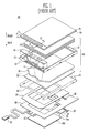
- FIG. 1 is an exploded perspective view showing a contemporary portable display device
- FIG. 2 is a coupled perspective view of part A illustrated in FIG. 1 ;
- FIG. 3 is a coupled cross-sectional view of a liquid crystal display panel, a backlight assembly, and a bottom chassis receiving them taken along line II-II' illustrated in FIG. 1 ;
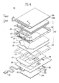
- FIG. 4 is an exploded perspective view showing a portable display device according to an embodiment of the principles of the present invention.
- FIG. 5 is a coupled perspective view of part C illustrated in FIG. 4 ;
- FIG. 6 is a view showing one example of the shape of an aperture formed in a mold frame surrounding a light-emitting diode.
- FIG. 7 is a coupled cross-sectional view of a liquid crystal display panel, a backlight assembly, and a bottom chassis receiving them taken along line III-III' illustrated in FIG. 4 .
- FIG. 1 is an exploded perspective view showing a conventional portable display device.
- a dual display device for use in, e.g. a cellular phone is constructed with at least one liquid crystal display device.
- FIG. 2 is a coupled perspective view of part A illustrated in FIG. 1
- FIG. 3 is a coupled cross-sectional view of a bottom chassis receiving a liquid crystal display panel and a backlight assembly taken along line II-II' in FIG. 1 .
- a light-emitting diode substrate is not shown in FIG. 2 .
- a conventional portable display device 60 is construed with a liquid crystal display panel 4, a backlight assembly 50, a bottom chassis 22, first and second printed circuit boards 24 and 26, and a light-emitting display panel 30.
- a liquid crystal display panel 4 which is a first display panel, displays a video image.
- liquid crystal display panel 4 is constructed with a first substrate 4a, a second substrate 4b and a liquid crystal (not shown) injected between first and second substrate 4a and 4b.
- the second substrate 4b is constructed with a plurality of thin film transistors (hereinafter, referred to as "TFT", which are not shown) disposed in a matrix shape.
- TFT thin film transistors
- source electrodes (not shown) of the TFTs are connected to a data line (not shown)
- gate electrodes (not shown) of the TFTs are connected to a scan line (not shown).
- Drain electrodes (not shown) of the TFTs are connected to a pixel electrode (not shown) made from an electrically conductive material, such as transparent indium tin oxide (ITO).
- ITO transparent indium tin oxide
- an integrated circuit 6 is inserted onto one side of second substrate 4b.
- the data signals and the scan signals are supplied from integrated circuit 6.
- a protective layer 8 is disposed on second substrate 4b, surrounding integrated circuit 6.
- the first substrate 4a is disposed to be opposite to the second substrate 4b.
- a common electrode made from ITO is applied to the front side of first substrate 4a.
- a certain voltage is applied to the common electrode, and accordingly, an electric field is formed between the common electrode and the pixel electrode.
- the array angle of the liquid crystal injected between the first substrate 4a and the second substrate 4b is changed by the electric field, and a light transmittance is changed due to the changes in the array angle, and thereby a desired image can be displayed.
- the upper and lower sides of the liquid crystal display panel 4 are further provided with upper and lower polarizing plates, respectively.
- the backlight assembly 50 is constructed with light-emitting diodes 12, a light-emitting diode substrate 14, a light guide plate 18, a reflecting plate 20, optical sheets 10 and a mold frame 16.
- the light-emitting diodes 12 are mounted on the light-emitting diode substrate 14 in a chip shape and generate light with a certain brightness corresponding to the driving signals supplied from light-emitting diode substrate 14.
- light-emitting diodes 12 function as a light source for the liquid crystal display device including the liquid crystal display panel 4 and the backlight assembly 50.
- At least one circuit component for example, a circuit component 13 supplying the driving signals to light-emitting diodes 12, is mounted on the light emitting diode substrate 14.
- the light guide plate 18 supplies light generated from the light-emitting diodes 12 to the liquid crystal display panel 4.
- the light guide plate 18 supplies light to the liquid crystal display panel 4 positioned at the upper side of the light guide plate 18, while the light is supplied from the side of the light guide plate 18.
- the thickness of the light guide plate 18 is set to be larger than or identical to the side thickness of the light-emitting diode 12. Accordingly, the thickness of the light guide plate 18 is set to be generally larger than that of the constituent included in the backlight assembly 50, such as optical sheets 10.
- the reflecting plate 20 which is positioned at the rear side of the light guide plate 18, re-supplies incident light received from light guide plate 18, to the light guide plate 18. In other words, the reflecting plate 20 improves the light efficiency by re-supplying received light incident from light guide plate 18, to light guide plate 18.
- the optical sheets 10 improve the brightness of the light supplied from light guide plate 18, and supply the light to the liquid crystal display panel 4.
- the light-emitting diode substrate 14 for mounting the light-emitting diode 12 is received and fixed in a mold frame 16, where the liquid crystal display panel 4 and the backlight assembly 50 are fixed and supported.
- the bottom chassis 22 is fixed at the lower side of the mold frame 16. At this time, an aperture 23 is formed in a part of the bottom chassis 22 so that the light-emitting display panel 30, which is the second display panel, can be inserted.
- the second printed circuit board 26 receives the driving signals from the driving circuit of the cellular phone, which is not shown. To this end, the second printed circuit board 26 is constructed with a cellular phone connector 28. The cellular phone connector 28 is united and fixed to another connector adhered to the driving circuit of the cellular phone to receive the driving signals from the driving circuit of the cellular phone. The second printed circuit board 26 for receiving the driving signals generates various control signals corresponding to the driving signals supplied to the second printed circuit board 26.
- the first printed circuit board 24 is connected to the second printed circuit board 26 through a first pad unit 38.
- the first printed circuit board 24 is connected to the integrated circuit 6 inserted onto the front side of the liquid crystal display panel 4 by a flexible printed circuit board, which is not shown.
- the first printed circuit board 24 connected to the integrated circuit 6 and the light-emitting diode substrate 14 drives the integrated circuit 6 and the light-emitting diode substrate 14 using the control signals supplied from the second printed circuit board 26.
- the light-emitting display panel 30, which is a second display panel, is constructed with a first substrate 30a and a second substrate 30b.
- Organic light-emitting diodes (not shown) are disposed on first substrate 30a in a matrix shape.
- the organic light-emitting diodes generate light of a certain brightness corresponding to the current supplied to the organic light-emitting diodes.
- the light-emitting display panel 30 is connected to the second printed circuit board 26 by means of a second pad unit 36 of the flexible printed circuit board 32.
- the integrated circuit 34 is inserted in flexible printed circuit board 32, and the integrated circuit 34 allows a video image to be displayed on the light-emitting display panel 30 by supplying the control signals from the second printed circuit board 26.
- the liquid crystal display panel 4 and the integrated circuit 6 may malfunction due to the heat generated when light-emitting diode 12 serves as a light source of the liquid crystal display device, and concomitantly emits light as well as attendant heat.
- a conventional portable display device 60 is designed so that the sides of the light-emitting diode 12 except the side adjacent to the light guide plate 18 are surrounded by the mold frame 16 in order to prevent light leakage.
- the heat generated from the light-emitting diode 12 fails to smoothly circulate so that the ambient temperature of light-emitting diode 12 maintains a high level.
- FIG. 4 is an exploded perspective view showing a portable display device constructed as an embodiment of the principles of the present invention.
- FIG. 4 shows a dual display device for use in a cellular phone and constructed with at least one liquid crystal display device; embodiments of the present invention are not limited thereto.
- FIG. 5 is a coupled perspective view of part C illustrated in FIG. 4 .
- a light-emitting diode substrate is not shown in FIG. 5 .
- a portable display device 160 is constructed with a liquid crystal display panel 104, a backlight assembly 150, a bottom chassis 122, first and second printed circuit boards 124 and 126, and a light-emitting display panel 30.
- the liquid crystal display panel 104 which is a first display panel, can display a video image.
- the liquid crystal display panel 104 is constructed with a first substrate 104a, a second substrate 104b and a liquid crystal (not shown) injected between the first and second substrates 104a and 104b .
- the second substrate 104b is constructed with a plurality of thin film transistors (hereinafter, referred to as a "TFT", which is not shown) disposed in a matrix shape.
- TFT thin film transistors
- source electrodes (not shown) of the TFTs are connected to a data line (not shown)
- gate electrodes (not shown) of the TFTs are connected to a scan line (not shown).
- Drain electrodes (not shown) of the TFTs are connected to pixel electrodes (not shown) made from an electrically conductive material, such as transparent indium tin oxide (ITO).
- ITO transparent indium tin oxide
- an integrated circuit 106 is inserted into one side of second substrate 104b.
- the data signals and the scan signals are supplied from integrated circuit 106.
- a protective layer 108 is applied to the surroundings of the integrated circuit 106.
- the first substrate 104a is disposed to be opposite to the second substrate 104b.
- a common electrode (not shown) made from ITO is disposed at the front side of the first substrate 104a.
- a certain voltage is applied to the common electrode and accordingly, a certain electric field is formed between the common electrode and the pixel electrode.
- the array angle of the liquid crystal injected between the first substrate 104a and the second substrate 104b is changed by the electric field, and the light transmittance is changed due to the changes in the array angle, therefore a desired image can be displayed.
- the upper and the lower sides of the liquid crystal display panel 104 are further provided with upper and lower polarizing plates, respectively.
- the backlight assembly 150 is constructed with a light source for supplying light to the liquid crystal display panel 104. More specifically, the backlight assembly 150 is constructed with light-emitting diodes 112, a light-emitting diode substrate 114, a light guide plate 118, a reflecting plate 120, optical sheets 110 and a mold frame 116.
- the light-emitting diodes 112 are mounted on the light-emitting diode substrate 114 in a chip shape and generate light with a certain brightness corresponding to the driving signals supplied from the light-emitting diode substrate 114.
- the light-emitting diodes 112 function as a light source for the liquid crystal display device including the liquid crystal display panel 104 and the backlight assembly 150.
- the light-emitting diode substrate 114 is connected to the first printed circuit board 124 and supplies the driving signals to the light-emitting diodes 112 by supplying the control signals supplied from the first printed circuit board 124.
- At least one circuit component for example, a circuit component 113 for supplying the driving signals to light-emitting diodes 112 may be further mounted on the light-emitting diode substrate 114.
- the light guide plate 118 positioned on one side of the light-emitting diodes 112 supplies light generated by the light-emitting diodes 112 to the liquid crystal display panel 104.
- the light guide plate 118 supplies light to the liquid crystal display panel 104 positioned at the upper side of light guide plate 118, and the light is supplied from the side of the light guide plate 118.
- the thickness of the light guide plate 118 is set to be larger than or identical to the thickness of the light-emitting diode 112. Accordingly, the thickness of light guide plate 118 is set to be generally larger than that of the constituent included in the backlight assembly 150, such as the optical sheets 110.
- the reflecting plate 120 which is positioned in the rear side of the light guide plate 118, re-supplies the light which is incident from the light guide plate 118, to the light guide plate 118. In other words, the reflecting plate 120 improves light efficiency by re-supplying the light which is incident from the light guide plate 118, to the light guide plate 118.
- the optical sheets 110 improve brightness of the light supplied from the light guide plate 118 and supply the light to the liquid crystal display panel 104.
- the mold frame 116 receives the liquid crystal display panel 104 and the backlight assembly 150. More specifically, in the mold frame 116, the liquid crystal display panel 104, light-emitting diode substrate 114 constructed with the light-emitting diode 114, which is a light source, the light guide plate 118, the reflecting plate 120 and the optical sheets 110, etc. are received.
- the bottom chassis 122 is fixed at the lower side of the mold frame 116 and receives the liquid crystal display panel 104 and the backlight assembly 150. At this time, an aperture 123 is formed in a part of the bottom chassis 122 so that the light-emitting display panel 130, which is the second display panel, can be inserted.
- the second printed circuit board 126 receives the driving signals from the driving circuit of the cellular phone, which is not shown.
- the second printed circuit board 126 is constructed with a cellular phone connector 128.
- the cellular phone connector 128 is united and fixed to another connector adhered to the driving circuit of the cellular phone and receives the driving signals from the driving circuit of the cellular phone.
- the second printed circuit board 126 is for receiving the driving signals and generates various control signals corresponding to the driving signals supplied from the second printed circuit board 126.
- the first printed circuit board 124 is connected to the second printed circuit board 126 through a first pad unit 138 formed on second printed circuit board 126.
- the first printed circuit board 124 is connected to the integrated circuit 106 of the liquid crystal display panel 104 and the light-emitting diode substrate 114 by a flexible printed circuit board, which is not shown.
- the first printed circuit board 124 connected to the integrated circuit 106 and the light-emitting diode substrate 114 drives the integrated circuit 106 and the light-emitting diode substrate 114 with the control signals supplied from the second printed circuit board 126.
- the light-emitting display panel 130 which is a second display panel, is constructed with a first substrate 130a and a second substrate 130b.
- Organic light-emitting diodes (not shown) in a matrix shape are disposed on the first substrate 130a.
- the organic light-emitting diodes generate light at a certain brightness corresponding to the current supplied to the organic light-emitting diodes.
- the light-emitting display panel 130 is connected to the second printed circuit board 126 by a second pad unit 136 of the flexible printed circuit board 132.
- the integrated circuit 134 is mounted on the flexible printed circuit board 132, and the integrated circuit 134 allows the light-emitting display panel 130 to display a image with the control signals from the second printed circuit board 126.
- the portable display device 160 is designed so that at least two sides of light-emitting diode 112, more preferably, all sides of light-emitting diode 112 except the side adjacent to light guide plate 118 are surrounded by the mold frame 116 in order to prevent light leakage.
- At least one region of the mold frame 116 surrounding the sides of the light-emitting diode 112 is constructed with at least one aperture 117 formed by through holes that completely perforates the mold frame 116.
- at least one region of the mold frame 116 surrounding the sides of light-emitting diode 112 may be constructed with four apertures 117. The apertures 117 may be formed during molding of mold frame 116.
- An aperture 117 which is to prevent the ambient temperature of the light-emitting diode 112 from being intensely raised by dispersing the heat, more specifically, by circulating the heated air generated when the light-emitting diode 112 emits the light, is formed in a tubular shape so as to penetrate mold frame 116.
- an aperture 117 may be formed in a tubular shape with a circular cross-section.
- the or each aperture 117 can be formed as annular holes.
- the cross-section of the apertures 117 is a circle in FIGS. 4 and 5
- the or each aperture 117 may be formed in various shapes.
- embodiments of the invention are not limited to a circular cross-section.
- the cross-section of the or each aperture 117 may be formed in a square shape.
- one aperture with a circular cross-section will now be discussed with reference to FIG. 6 .
- FIG. 6 is a view showing one example of the shape of an aperture formed in a mold frame surrounding a light-emitting diode. Combining FIG. 5 and FIG. 6 , the principle for heat dissipation by circulating air will be described below.
- the aperture 117 formed in at least one region of mold frame 116 surrounding the light-emitting diode 112 is formed in a tubular shape having a circular cross-section. The heat generated by light-emitting diode 112 is dispersed through the aperture 117.
- the ambient air of the light-emitting diode 112 i.e. the air around the light-emitting diode 112
- the density of the heated air lowers and causes natural convection.
- the heat transfer rate Q1 by means of such natural convection is defined by the following mathematical equation.
- Q ⁇ 1 hA s ⁇ T s - T ⁇
- T s represents the surface temperature of the light-emitting diode 112 in this embodiment.
- T ⁇ is the temperature of fluid, which is sufficiently apart from the surface of light-emitting diode 112.
- T ⁇ represents the temperature of the air in the space which is external to the space between the light-emitting diode 112 and the mold frame 116 surrounding the light-emitting diode 112.
- T ⁇ represents the temperature of the air in the space which is at the side of the aperture 117 opposite to the side where the space between the light-emitting diode 112 and the mold frame 116 surrounding light-emitting diode 112 is located.
- a s represents the surface area of the aperture 117, that is, the surface area of the inner tube of the aperture 117 formed in a tubular shape.
- the surface area A s of aperture 117 is defined by the following mathematical equation 2, where the diameter of the circular cross-section of aperture 117 is D and the length of the aperture 117 is L.
- a s ⁇ DL
- h in equation 1 represents a convection heat transfer coefficient, and may be calculated by mathematical equation 3.
- h k D ⁇ Nu
- Nusselt number Nu is defined as a dimensionless number characterizing the relationship between temperature field and heat transfer intensity on a boundary layer of flow, and is a dimensionless number representing the rate of heat exchange between the fluid (that is, the air) and the solid (that is, a tube wall of the aperture).
- Pr represents the Prandtl number which is a ratio of momentum diffusivity and the thermal diffusivity.
- Prandtl number Pr is a criterion for a relative value of momentum and energy transfer by means of diffusion in a velocity boundary layer and a motion boundary layer.
- g acceleration due to gravity and ⁇ represents volumetric expansion coefficients. ⁇ equals 1 / T in an ideal gas. Also, ⁇ represents the kinematic viscosity of fluid (that is, for example, air).
- the convective heat transfer rate Q1 may be controlled by the diameter D of the circular cross-section, the length L of the aperture 117, and the number of aperture 117.
- embodiments of the present invention can control the desired convective heat transfer rate Q1 in a certain condition by means of the shape, the size and the number of apertures 117.
- Heat transfer rate due to radiation is also proportional to surface area A s of the aperture 117 so that it can also be controlled by means of the shape, the size and the number of aperture 117.
- embodiments of the present invention can prevent the ambient temperature of light-emitting diode 112 from being intensely raised by forming at least one aperture 117 in mold frame 116 in order to obtain the desired convective heat transfer rate Q1 and radiative heat transfer rate.
- embodiments of the present invention include at least one aperture 117 formed on the mold frame surrounding the light-emitting diode 112 so that deterioration of elements positioned adjacent to the light-emitting diode 112 can be prevented by dispersing heat generated from the light-emitting diode 112.
- embodiments of the present invention can prevent the ambient temperature of the light-emitting diode 112 from being intensely raised by dissipating the heat generated by the light-emitting diode 112. Thereby, embodiments of the present invention do not greatly heat parts of the liquid crystal display panel 104 so that deterioration of the liquid crystal display panel 104, in particular, the liquid crystal injected therebetween, and elements included in integrated circuit 106 can be prevented. Also, although not shown in FIG. 7 , when at least one circuit component 113 illustrated in FIG. 4 is mounted on the light-emitting diode substrate 114, such a circuit component 113 is also protected from deterioration due to a high temperature.
- apertures 117 with a cross-sectional shape of a circle are used in some embodiments of the present invention, the present invention is not limited thereto.
- the surface area of the inner tube of aperture 117 can be calculated so that various shapes of aperture 117 can be formed on the mold frame in order to obtain the desired convective heat transfer rate Q1 and radiative heat transfer heat. Thereby, it is possible to prevent the ambient temperature of light-emitting diode 112 from being intensely raised.
- a portable display device can disperse heat by circulating air heated by means of heat generated when the light source emits the light, by the formation at least one aperture in the mold frame surrounding the sides of the light source in the portable display device with the liquid crystal display device.
- embodiments of the present invention prevent the ambient temperature of the light source from being intensely raised. Accordingly, embodiments of the present invention can prevent deterioration of elements positioned adjacent to the light source, for example, the liquid crystal display panel and the integrated circuit thereof, and the circuit components included in the substrate mounting the light source.
Landscapes
- Physics & Mathematics (AREA)
- Nonlinear Science (AREA)
- General Physics & Mathematics (AREA)
- Optics & Photonics (AREA)
- Mathematical Physics (AREA)
- Chemical & Material Sciences (AREA)
- Crystallography & Structural Chemistry (AREA)
- Liquid Crystal (AREA)
- Devices For Indicating Variable Information By Combining Individual Elements (AREA)
- Planar Illumination Modules (AREA)
Applications Claiming Priority (1)
| Application Number | Priority Date | Filing Date | Title |
|---|---|---|---|
| KR1020060110569A KR100836488B1 (ko) | 2006-11-09 | 2006-11-09 | 휴대용 표시장치 |
Publications (2)
| Publication Number | Publication Date |
|---|---|
| EP1921494A2 true EP1921494A2 (de) | 2008-05-14 |
| EP1921494A3 EP1921494A3 (de) | 2010-03-31 |
Family
ID=39204745
Family Applications (1)
| Application Number | Title | Priority Date | Filing Date |
|---|---|---|---|
| EP07254419A Ceased EP1921494A3 (de) | 2006-11-09 | 2007-11-09 | Tragbare Anzeigevorrichtung |
Country Status (5)
| Country | Link |
|---|---|
| US (1) | US7924361B2 (de) |
| EP (1) | EP1921494A3 (de) |
| JP (1) | JP4612002B2 (de) |
| KR (1) | KR100836488B1 (de) |
| CN (1) | CN101178499A (de) |
Families Citing this family (10)
| Publication number | Priority date | Publication date | Assignee | Title |
|---|---|---|---|---|
| CN101529324B (zh) * | 2006-11-06 | 2011-02-02 | 松下电器产业株式会社 | 液晶显示装置 |
| EP2153273B1 (de) * | 2007-06-01 | 2017-05-10 | LG Display Co., Ltd. | Anzeigevorrichtung |
| US12185512B2 (en) | 2007-11-16 | 2024-12-31 | Manufacturing Resources International, Inc. | Electronic display assembly with thermal management |
| TWI408442B (zh) * | 2010-04-15 | 2013-09-11 | Au Optronics Corp | 液晶顯示裝置 |
| TWI468790B (zh) * | 2013-12-12 | 2015-01-11 | Au Optronics Corp | 顯示模組 |
| KR102501607B1 (ko) * | 2015-12-23 | 2023-02-17 | 엘지디스플레이 주식회사 | 액정 표시 장치 |
| US11778757B2 (en) | 2020-10-23 | 2023-10-03 | Manufacturing Resources International, Inc. | Display assemblies incorporating electric vehicle charging equipment |
| US11966263B2 (en) | 2021-07-28 | 2024-04-23 | Manufacturing Resources International, Inc. | Display assemblies for providing compressive forces at electronic display layers |
| US11968813B2 (en) | 2021-11-23 | 2024-04-23 | Manufacturing Resources International, Inc. | Display assembly with divided interior space |
| US20250189117A1 (en) * | 2023-12-08 | 2025-06-12 | Carolina Moore | Illuminated ruler and manufacture method thereof |
Citations (2)
| Publication number | Priority date | Publication date | Assignee | Title |
|---|---|---|---|---|
| JPH11119216A (ja) * | 1997-10-14 | 1999-04-30 | I O Data Device Inc | 液晶ディスプレイ |
| US20030164903A1 (en) * | 2002-01-24 | 2003-09-04 | Ken Saito | Liquid crystal display device |
Family Cites Families (18)
| Publication number | Priority date | Publication date | Assignee | Title |
|---|---|---|---|---|
| JP2000227594A (ja) * | 1999-02-08 | 2000-08-15 | Citizen Watch Co Ltd | 液晶表示装置 |
| TWI243940B (en) * | 2000-11-01 | 2005-11-21 | Au Optronics Corp | Housing for flat panel display and method for assembly the same |
| JP2002162626A (ja) * | 2000-11-22 | 2002-06-07 | Sony Corp | 液晶表示用光源の放熱装置及びその製造方法 |
| KR100688677B1 (ko) * | 2001-12-25 | 2007-03-02 | 마츠시타 덴끼 산교 가부시키가이샤 | 조명 유닛 및 그것을 이용한 액정 표시 장치 |
| TW564302B (en) * | 2002-08-09 | 2003-12-01 | Au Optronics Corp | Back light unit with high heat transfer rate |
| US7367706B2 (en) * | 2002-09-19 | 2008-05-06 | Toshiba Matsushita Display Technology Co., Ltd. | Illumination unit and liquid crystal display comprising it |
| TWI252348B (en) * | 2002-10-21 | 2006-04-01 | Toppoly Optoelectronics Corp | Back light module |
| KR100970261B1 (ko) * | 2003-05-31 | 2010-07-16 | 삼성전자주식회사 | 백라이트 어셈블리 및 이를 갖는 액정표시장치 |
| KR20050073999A (ko) * | 2004-01-13 | 2005-07-18 | 삼성전자주식회사 | 방열용 바텀 샤시를 구비하는 액정표시장치 |
| KR20060032398A (ko) * | 2004-10-12 | 2006-04-17 | 삼성전자주식회사 | 평판표시장치 |
| KR100638047B1 (ko) * | 2004-10-15 | 2006-10-23 | 엘지전자 주식회사 | 백라이트 유닛을 갖는 액정 디스플레이 |
| DE102005063433B4 (de) | 2004-10-29 | 2009-11-26 | Lg Display Co., Ltd. | Hintergrundbeleuchtungseinheit und Flüssigkristall-Anzeigevorrichtung |
| KR101107997B1 (ko) * | 2004-11-17 | 2012-01-31 | 삼성전자주식회사 | 백라이트 유닛 및 이를 갖는 표시장치 |
| TWI261696B (en) * | 2005-01-10 | 2006-09-11 | Au Optronics Corp | Liquid crystal display and backlight module thereof |
| KR20060090387A (ko) * | 2005-02-07 | 2006-08-10 | 삼성전자주식회사 | 방열 효율을 향상시킨 백라이트 어셈블리 및 이를 구비한평판표시장치 |
| US7262438B2 (en) | 2005-03-08 | 2007-08-28 | Avago Technologies Ecbu Ip (Singapore) Pte. Ltd. | LED mounting having increased heat dissipation |
| TWI268388B (en) * | 2005-03-11 | 2006-12-11 | Au Optronics Corp | Backlight module |
| KR101134302B1 (ko) * | 2005-06-30 | 2012-04-13 | 엘지디스플레이 주식회사 | 액정표시장치용 커버버툼 및 이를 이용한 발광다이오드백라이트어셈블리와 액정표시장치모듈 |
-
2006
- 2006-11-09 KR KR1020060110569A patent/KR100836488B1/ko not_active Expired - Fee Related
-
2007
- 2007-01-10 JP JP2007002349A patent/JP4612002B2/ja not_active Expired - Fee Related
- 2007-04-24 US US11/790,217 patent/US7924361B2/en active Active
- 2007-10-08 CN CNA2007101627284A patent/CN101178499A/zh active Pending
- 2007-11-09 EP EP07254419A patent/EP1921494A3/de not_active Ceased
Patent Citations (2)
| Publication number | Priority date | Publication date | Assignee | Title |
|---|---|---|---|---|
| JPH11119216A (ja) * | 1997-10-14 | 1999-04-30 | I O Data Device Inc | 液晶ディスプレイ |
| US20030164903A1 (en) * | 2002-01-24 | 2003-09-04 | Ken Saito | Liquid crystal display device |
Also Published As
| Publication number | Publication date |
|---|---|
| JP4612002B2 (ja) | 2011-01-12 |
| KR20080042318A (ko) | 2008-05-15 |
| JP2008122894A (ja) | 2008-05-29 |
| KR100836488B1 (ko) | 2008-06-09 |
| US7924361B2 (en) | 2011-04-12 |
| EP1921494A3 (de) | 2010-03-31 |
| CN101178499A (zh) | 2008-05-14 |
| US20080111936A1 (en) | 2008-05-15 |
Similar Documents
| Publication | Publication Date | Title |
|---|---|---|
| EP1921494A2 (de) | Tragbare Anzeigevorrichtung | |
| CN1991459B (zh) | 显示装置 | |
| KR101189135B1 (ko) | 액정표시장치모듈 | |
| TWI461796B (zh) | 液晶顯示裝置 | |
| KR20130027335A (ko) | 액정표시장치 및 이의 제조방법 | |
| KR100762689B1 (ko) | 휴대용 표시장치 | |
| US20110110046A1 (en) | Reinforcement frame, component unit, and display | |
| CN103578365A (zh) | 显示装置 | |
| CN102024405B (zh) | 平板显示器 | |
| JP5537860B2 (ja) | 表示装置 | |
| US10429686B2 (en) | Heat dissipation module and liquid crystal display | |
| KR20110066798A (ko) | 액정표시장치 | |
| CN101814255B (zh) | 显示装置 | |
| JP4376269B2 (ja) | 携帯用表示装置 | |
| KR100722120B1 (ko) | 휴대용 표시장치 | |
| KR20080003034A (ko) | 액정표시모듈 | |
| JP4631330B2 (ja) | 画像表示装置 | |
| KR101621557B1 (ko) | 액정표시장치 | |
| KR101854916B1 (ko) | 백라이트 유닛 및 이를 구비한 액정표시장치 | |
| KR20250003190A (ko) | 디스플레이 장치 | |
| KR100793533B1 (ko) | 휴대용 표시장치 | |
| CN116367605A (zh) | 显示设备 | |
| KR20060127365A (ko) | 액정표시장치 | |
| KR20060118963A (ko) | 플라즈마 디스플레이 장치 | |
| KR20070117895A (ko) | 휴대용 표시장치 |
Legal Events
| Date | Code | Title | Description |
|---|---|---|---|
| PUAI | Public reference made under article 153(3) epc to a published international application that has entered the european phase |
Free format text: ORIGINAL CODE: 0009012 |
|
| 17P | Request for examination filed |
Effective date: 20071116 |
|
| AK | Designated contracting states |
Kind code of ref document: A2 Designated state(s): AT BE BG CH CY CZ DE DK EE ES FI FR GB GR HU IE IS IT LI LT LU LV MC MT NL PL PT RO SE SI SK TR |
|
| AX | Request for extension of the european patent |
Extension state: AL BA HR MK RS |
|
| RAP1 | Party data changed (applicant data changed or rights of an application transferred) |
Owner name: SAMSUNG MOBILE DISPLAY CO., LTD. |
|
| PUAL | Search report despatched |
Free format text: ORIGINAL CODE: 0009013 |
|
| AK | Designated contracting states |
Kind code of ref document: A3 Designated state(s): AT BE BG CH CY CZ DE DK EE ES FI FR GB GR HU IE IS IT LI LT LU LV MC MT NL PL PT RO SE SI SK TR |
|
| AX | Request for extension of the european patent |
Extension state: AL BA HR MK RS |
|
| AKX | Designation fees paid |
Designated state(s): DE FR GB |
|
| 17Q | First examination report despatched |
Effective date: 20101215 |
|
| STAA | Information on the status of an ep patent application or granted ep patent |
Free format text: STATUS: THE APPLICATION HAS BEEN REFUSED |
|
| 18R | Application refused |
Effective date: 20110927 |