EP1921570A2 - Étiquette de circuit intégré à fréquence radio et procédé d'utilisation de l'étiquette RFIC/RFID - Google Patents
Étiquette de circuit intégré à fréquence radio et procédé d'utilisation de l'étiquette RFIC/RFID Download PDFInfo
- Publication number
- EP1921570A2 EP1921570A2 EP07008137A EP07008137A EP1921570A2 EP 1921570 A2 EP1921570 A2 EP 1921570A2 EP 07008137 A EP07008137 A EP 07008137A EP 07008137 A EP07008137 A EP 07008137A EP 1921570 A2 EP1921570 A2 EP 1921570A2
- Authority
- EP
- European Patent Office
- Prior art keywords
- chip
- rfic tag
- impedance matching
- metal object
- antenna
- Prior art date
- Legal status (The legal status is an assumption and is not a legal conclusion. Google has not performed a legal analysis and makes no representation as to the accuracy of the status listed.)
- Granted
Links
Images




Classifications
-
- G—PHYSICS
- G06—COMPUTING OR CALCULATING; COUNTING
- G06K—GRAPHICAL DATA READING; PRESENTATION OF DATA; RECORD CARRIERS; HANDLING RECORD CARRIERS
- G06K19/00—Record carriers for use with machines and with at least a part designed to carry digital markings
- G06K19/06—Record carriers for use with machines and with at least a part designed to carry digital markings characterised by the kind of the digital marking, e.g. shape, nature, code
- G06K19/067—Record carriers with conductive marks, printed circuits or semiconductor circuit elements, e.g. credit or identity cards also with resonating or responding marks without active components
- G06K19/07—Record carriers with conductive marks, printed circuits or semiconductor circuit elements, e.g. credit or identity cards also with resonating or responding marks without active components with integrated circuit chips
- G06K19/077—Constructional details, e.g. mounting of circuits in the carrier
-
- G—PHYSICS
- G06—COMPUTING OR CALCULATING; COUNTING
- G06K—GRAPHICAL DATA READING; PRESENTATION OF DATA; RECORD CARRIERS; HANDLING RECORD CARRIERS
- G06K19/00—Record carriers for use with machines and with at least a part designed to carry digital markings
- G06K19/06—Record carriers for use with machines and with at least a part designed to carry digital markings characterised by the kind of the digital marking, e.g. shape, nature, code
- G06K19/067—Record carriers with conductive marks, printed circuits or semiconductor circuit elements, e.g. credit or identity cards also with resonating or responding marks without active components
- G06K19/07—Record carriers with conductive marks, printed circuits or semiconductor circuit elements, e.g. credit or identity cards also with resonating or responding marks without active components with integrated circuit chips
- G06K19/077—Constructional details, e.g. mounting of circuits in the carrier
- G06K19/07745—Mounting details of integrated circuit chips
-
- G—PHYSICS
- G06—COMPUTING OR CALCULATING; COUNTING
- G06K—GRAPHICAL DATA READING; PRESENTATION OF DATA; RECORD CARRIERS; HANDLING RECORD CARRIERS
- G06K19/00—Record carriers for use with machines and with at least a part designed to carry digital markings
- G06K19/06—Record carriers for use with machines and with at least a part designed to carry digital markings characterised by the kind of the digital marking, e.g. shape, nature, code
- G06K19/067—Record carriers with conductive marks, printed circuits or semiconductor circuit elements, e.g. credit or identity cards also with resonating or responding marks without active components
- G06K19/07—Record carriers with conductive marks, printed circuits or semiconductor circuit elements, e.g. credit or identity cards also with resonating or responding marks without active components with integrated circuit chips
-
- G—PHYSICS
- G06—COMPUTING OR CALCULATING; COUNTING
- G06K—GRAPHICAL DATA READING; PRESENTATION OF DATA; RECORD CARRIERS; HANDLING RECORD CARRIERS
- G06K19/00—Record carriers for use with machines and with at least a part designed to carry digital markings
- G06K19/06—Record carriers for use with machines and with at least a part designed to carry digital markings characterised by the kind of the digital marking, e.g. shape, nature, code
- G06K19/067—Record carriers with conductive marks, printed circuits or semiconductor circuit elements, e.g. credit or identity cards also with resonating or responding marks without active components
- G06K19/07—Record carriers with conductive marks, printed circuits or semiconductor circuit elements, e.g. credit or identity cards also with resonating or responding marks without active components with integrated circuit chips
- G06K19/077—Constructional details, e.g. mounting of circuits in the carrier
- G06K19/07749—Constructional details, e.g. mounting of circuits in the carrier the record carrier being capable of non-contact communication, e.g. constructional details of the antenna of a non-contact smart card
-
- G—PHYSICS
- G06—COMPUTING OR CALCULATING; COUNTING
- G06K—GRAPHICAL DATA READING; PRESENTATION OF DATA; RECORD CARRIERS; HANDLING RECORD CARRIERS
- G06K19/00—Record carriers for use with machines and with at least a part designed to carry digital markings
- G06K19/06—Record carriers for use with machines and with at least a part designed to carry digital markings characterised by the kind of the digital marking, e.g. shape, nature, code
- G06K19/067—Record carriers with conductive marks, printed circuits or semiconductor circuit elements, e.g. credit or identity cards also with resonating or responding marks without active components
- G06K19/07—Record carriers with conductive marks, printed circuits or semiconductor circuit elements, e.g. credit or identity cards also with resonating or responding marks without active components with integrated circuit chips
- G06K19/077—Constructional details, e.g. mounting of circuits in the carrier
- G06K19/07749—Constructional details, e.g. mounting of circuits in the carrier the record carrier being capable of non-contact communication, e.g. constructional details of the antenna of a non-contact smart card
- G06K19/0775—Constructional details, e.g. mounting of circuits in the carrier the record carrier being capable of non-contact communication, e.g. constructional details of the antenna of a non-contact smart card arrangements for connecting the integrated circuit to the antenna
- G06K19/07756—Constructional details, e.g. mounting of circuits in the carrier the record carrier being capable of non-contact communication, e.g. constructional details of the antenna of a non-contact smart card arrangements for connecting the integrated circuit to the antenna the connection being non-galvanic, e.g. capacitive
-
- G—PHYSICS
- G06—COMPUTING OR CALCULATING; COUNTING
- G06K—GRAPHICAL DATA READING; PRESENTATION OF DATA; RECORD CARRIERS; HANDLING RECORD CARRIERS
- G06K19/00—Record carriers for use with machines and with at least a part designed to carry digital markings
- G06K19/06—Record carriers for use with machines and with at least a part designed to carry digital markings characterised by the kind of the digital marking, e.g. shape, nature, code
- G06K19/067—Record carriers with conductive marks, printed circuits or semiconductor circuit elements, e.g. credit or identity cards also with resonating or responding marks without active components
- G06K19/07—Record carriers with conductive marks, printed circuits or semiconductor circuit elements, e.g. credit or identity cards also with resonating or responding marks without active components with integrated circuit chips
- G06K19/077—Constructional details, e.g. mounting of circuits in the carrier
- G06K19/07749—Constructional details, e.g. mounting of circuits in the carrier the record carrier being capable of non-contact communication, e.g. constructional details of the antenna of a non-contact smart card
- G06K19/07771—Constructional details, e.g. mounting of circuits in the carrier the record carrier being capable of non-contact communication, e.g. constructional details of the antenna of a non-contact smart card the record carrier comprising means for minimising adverse effects on the data communication capability of the record carrier, e.g. minimising Eddy currents induced in a proximate metal or otherwise electromagnetically interfering object
-
- G—PHYSICS
- G06—COMPUTING OR CALCULATING; COUNTING
- G06K—GRAPHICAL DATA READING; PRESENTATION OF DATA; RECORD CARRIERS; HANDLING RECORD CARRIERS
- G06K19/00—Record carriers for use with machines and with at least a part designed to carry digital markings
- G06K19/06—Record carriers for use with machines and with at least a part designed to carry digital markings characterised by the kind of the digital marking, e.g. shape, nature, code
- G06K19/067—Record carriers with conductive marks, printed circuits or semiconductor circuit elements, e.g. credit or identity cards also with resonating or responding marks without active components
- G06K19/07—Record carriers with conductive marks, printed circuits or semiconductor circuit elements, e.g. credit or identity cards also with resonating or responding marks without active components with integrated circuit chips
- G06K19/077—Constructional details, e.g. mounting of circuits in the carrier
- G06K19/07749—Constructional details, e.g. mounting of circuits in the carrier the record carrier being capable of non-contact communication, e.g. constructional details of the antenna of a non-contact smart card
- G06K19/07773—Antenna details
- G06K19/07786—Antenna details the antenna being of the HF type, such as a dipole
Definitions
- the present invention relates to an RFIC tag attached to a metal object and a method of using the RFIC tag.
- an RFIC Radio Frequency Integrated Circuit
- data is communicated via a radio wave between an RFIC tag, which contains an IC chip activated by a radio wave, and a reader, a writer, or a reader/writer (hereinafter generically called a reader/writer).
- a reader/writer a reader/writer
- this RFIC system uses an antenna, provided both on an RFIC tag and a reader/writer, for data communication to allow data to be communicated even if the RFIC tag is away from the reader/writer and because an RFIC tag is resistant to stain, the system finds various applications in production management in a factory, physical distribution management, room entry/exit management, and so on.
- An RFIC tag having a dipole antenna and operating in the UHF band or SHF band does not work when it is placed near to a metal, for example, when it is placed directly on a metal object. Therefore, when an RFIC tag is attached to a metal object, a spacer made of plastic or rubber is provided between an RFIC tag and a metal object to keep spacing between the metal object and the antenna for suppressing the effect of the metal.
- the problem is that, if a thinner spacer is used to narrow the spacing between the surface of the metal object and the antenna, the RFIC does not work. On the other hand, if a thick spacer is used to increase the spacing between the metal object and the antenna, the communication distance is extended but the RFIC tag protrudes from the surface of the metal object and, in this case, there is a possibility that the metal object, when used, strikes against a surrounding object or against another metal object with the result that the RFIC tag is damaged.
- JP-A-2005-309811 discloses an RFIC tag in which a soft magnetic material is provided on the mounting face of the metal object on which the dipole antenna is attached, or a soft magnetic material and a spacer are provided from the metal object side on the mounting face of the metal object on which the dipole antenna is attached, or a spacer, a soft magnetic material, and a spacer are provided from the metal object side on the mounting face of the metal object on which the dipole antenna is attached.
- an IC chip is mounted on a dipole antenna which is, in turn, mounted on the metal object.
- This structure has a disadvantage in that an antenna that is half-wavelength ( ⁇ /2) long, where ⁇ is the communication wavelength, is required and therefore the RFIC tag becomes larger.
- An RFIC tag in a first aspect of the present invention is an RFIC tag having an IC chip, which is activated by a radio wave, mounted on a conductive thin plate or thin film.
- the conductive thin plate or thin film is mounted in such a way that connecting parts, provided at both ends thereof, are connected to a metal object electrically or via electrostatic capacitory coupling to cause the metal object to work as an antenna of the IC chip.
- the conductive thin plate or thin film has an impedance matching circuit in an intermediate part for matching an impedance of the antenna with an impedance of the IC chip.
- the impedance matching circuit is mounted with at least a predetermined spacing from the metal object. The length of the impedance matching circuit is shorter than ⁇ /2 where ⁇ is a wavelength of a radio wave to be transmitted or received.
- the metal surface of the metal object can be used as the antenna of the IC chip, the communication can be performed with the thin plate, on which the IC chip is mounted, as an RFIC tag, even if the length of the impedance matching circuit on the conductive thin plate or thin film, on which the IC chip is mounted, is shorter than 1/2 of the communication wavelength ⁇ of the IC chip.
- An RFIC tag in a second aspect of the present invention is a small inlet-type RFIC tag including an IC chip activated by a radio wave and a small antenna having an impedance matching circuit.
- the connecting parts, provided at predetermined ends of the small antenna, are connected to a metal object electrically or via electrostatic capacitory coupling to cause the metal object to work as an antenna of the IC chip.
- the impedance matching circuit is mounted with at least a predetermined spacing from the metal object. The length of the impedance matching circuit of the small antenna is shorter than ⁇ /2 where is the wavelength of a radio wave to be transmitted or received.
- the metal surface of the metal object can be used as the antenna of the IC chip, the communication can be performed with the small inlet as an RFIC tag, even if the length of the small antenna of the small inlet is shorter than 1/2 of the communication wavelength ⁇ of the IC chip.
- the present invention also includes the using method of the RFIC tag.
- a small RFIC tag that can be mounted on a metal object is provided.
- FIG. 1A is a perspective view showing an RFIC tag in the first embodiment mounted on a metal member (metal object)
- FIG. 1B is a top view of the RFIC tag from which an IC chip is removed
- FIG. 1C is a cross sectional view taken on the arrow line X1-X1 in FIG. 1A
- FIG. 1D is an equivalent circuit diagram of the RFIC tag.
- An RFIC tag 1A includes an IC chip 5 and a thin metal plate (thin conductive plate) 10A of copper (Cu) or aluminum (Al). As shown in FIG. 1A, the IC chip 5 is mounted approximately in the center of a part (hereinafter called a slit part) 10a that is the intermediate part in the longitudinal direction of the thin metal plate 10A where an impedance matching circuit is provided.
- a slit part a part
- the thin metal plate 10A is structured in such a way that connecting parts 10c at both longitudinal-direction ends are fixed on a metal member 2 by a conductive adhesive or welding such as soldering, not shown, and that the undersurface of the slit part 10a is lifted a predetermined height h (for example, 100 ⁇ m or higher) above the surface of the metal member 2 by means of feet 10b that are bent approximately at a right angle.
- a predetermined height h for example, 100 ⁇ m or higher
- the slit part 10a has a slit 6A that is a cut extending from approximately the midpoint of one of the long sides to approximately the half of the width and, in addition, bent at a right angle into the longitudinal direction to form an L shape when viewed from top.
- the IC chip 5 is mounted on the thin metal plate 10A, for example, by electrically connecting through ultrasonic bonding, so that signal input/output electrodes 5a and 5b, which are terminals for supplying power to the antenna of the IC chip 5, correspond to the positions 5a and 5b indicated by the rectangles, that is, so that the signal input/output electrodes are opposed each other across the slit 6A (see FIG. 1C).
- the thin metal plate 10A is, for example, 100 ⁇ m thick.
- the thin metal plate 10A should be strong enough for the slit part 10a to be supported a predetermined height from the surface of the metal member 2, and the thickness of the thin metal plate 10A should be appropriately determined according to its material.
- the longitudinal length L1 of the slit part 10a is, for example, 7mm or longer that is the longitudinal length of the L-shaped slit 6A (for example, 3.5mm (see FIG. 1B)) plus the length, equal to the width of the IC chip 5, at both ends in the longitudinal direction.
- the length L2 of the connecting part 10c is, for example, about 5mm.
- the total length L2+L1+L2 is about 17mm ( ⁇ /7 or shorter in terms of wavelength ⁇ ).
- the experiment shows that the length L1 of about 20mm and the total length L2+L1+L2 of about 30mm make the communication length relatively long.
- the numeric values given above are those for a configuration where the longitudinal width of the IC chip 5 is about 0.5mm and the communication frequency of the IC chip 5 is 2.45GHz.
- the length of the slit 6A that is, the length L1 of the slit part 10a, should be appropriately set according to the level of the impedance matching.
- the connecting part 10c is electrically connected to the surface of the metal member 2 by soldering
- the length L2 may be any length but, when the connecting part 10c is pasted by an insulating adhesive, that is, when connected through electrostatic capacity coupling, the length L2 should be about 5mm.
- the part of a stub 6a is connected in series between the slit part 10a, which works as an antenna, the metal member 2, and the IC chip 5.
- the part of this stub 6a works as a series-connected inductance component. This inductance component cancels the capacitive component in the IC chip 5 for better impedance matching between the antenna and the IC chip 5.
- the IC chip 5 can use the enough-area metal member 2 as the antenna and, at the same time, match the impedance of the IC chip 5 with the impedance of the antenna formed by the slit part 10a and the metal member 2.
- a slit part 10a including such the slit 6A is called an impedance matching circuit.
- the impedance matching is determined by the inductance component of the stub 6a which is determined by the lengths to the corner of the L shape of the slit 6A.
- the longitudinal length of the slit part 10a of the RFIC tag 1A is as short as 1/4 or less of the communication wavelength ⁇ . Even if the length, whose minimum total length is about 17mm, is extended preferably to about 30mm to extend the communication distance, the longitudinal length is 1/4 or less of the wavelength ⁇ , - meaning that the communication can be performed via the small RFIC tag 1A.
- the communication can be performed with the thin metal plate, on which the IC chip 5 is mounted, as an RFIC tag even if the length of the thin metal plate, on which the IC chip 5 including the impedance matching circuit is mounted, is shorter than 1/2 of the communication wavelength ⁇ of the IC chip 5.
- the spacing 100 ⁇ m or longer, is only required between the undersurface of the slit part 10a and the metal member 2 to allow it to work as the impedance matching circuit, the protrusion from the surface of the metal member 2 is small and thus the RFIC tag 1A is less likely to be hung when used.
- the metal member 2 to which the RFIC tag 1A in this embodiment is applicable is conductive metal such as aluminum (Al), carbon steel, stainless steel, and copper (Cu). Note that the RFIC tag 1A in this embodiment is applicable to stainless steel whether it is magnetic or not.
- the present invention is not limited to it.
- a thin plate composed of a conductive thin plate or a conductive resin, which has a conductive thin metal film thereon formed through plating, disposition, or spattering on the surface of a resin plate, may also be used.
- FIG. 2A shows an RFIC tag 1B whose feet 10b of a thin metal plate 10B are mounted at a setting angle different from that of the feet 10b of the RFIC tag 1A so that the feet are obliquely widen toward the bottom.
- Setting the angle of the feet 10b of the thin metal plate 10B as shown in FIG. 2A has an advantage that, when a hard material is used for the thin metal plate 10B, prevents the plate from being broken when it is bent.
- FIG. 2B shows an RFIC tag 1C whose feet 10b and connecting parts 10c of a thin metal plate 10C are extended in the width direction from a total of four positions, that is, from both width-direction ends of the longitudinal-direction ends of the slit part 10a. Arranging the feet 10b and the connecting parts 10c in this way maintains the spacing between the slit part 10a in the intermediate part and the metal member 2 more reliably.
- FIG. 3A shows an RFIC tag similar to the RFIC tag 1A except only in that the connecting parts 10c are bent inward at a right angle with respect to the feet 10b of a thin metal plate 10D so that the connecting parts 10c are positioned below the slit part 10a.
- This mounting form makes the longitudinal direction part more compact than that in the first embodiment.
- the connecting parts 10c having this form ensures easy electrical connection with the metal member 2.
- FIG. 3B shows an RFIC tag 1E whose feet 10b are mounted at a setting angle different from that of the feet 10b in FIG. 3A so that the feet are obliquely widen toward the bottom.
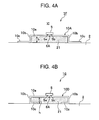
- FIG. 4A shows an RFIC tag 1F mounted on the metal member 2 with a spacer member 21 of an insulating material provided on the undersurface (mounting face) of the slit part 10a of the RFIC tag 1A.
- FIG. 4B shows an RFIC tag 1G mounted on the metal member 2 with a spacer member 21 of an insulating material provided below the slit part 10a of the RFIC tag 1D.
- the material of the spacer member 21 is preferably a resin thin plate of polyethylene terepthalate (PET) or polypropylene (PP) that is pasted on the undersurface of the slit part 10a with an adhesive material not shown.
- PET polyethylene terepthalate
- PP polypropylene
- ceramic or epoxy resin which is used for the package material of a semiconductor, for the spacer member 21 and packaging the whole RFIC tag 1F in the same way the parts, called a chip resistor or a chip capacitor, are packaged make the RFIC tag still easier to handle.
- the RFIC tag 1F and the RFIC tag 1G which have the spacer member 21 provided below the slit part 10a, have an advantage in that the spacing between the slit part 10a and the surface of the metal member 2 is not changed even if an external force is applied to the slit part 10a. That is, this structure prevents the thin metal plate 10A or 10D from being plastic-deformed and prevents the communication distance from being changed.
- FIG. 5A shows an RFIC tag 1H, a modification of the RFIC tag IC shown in FIG. 2B, in which the feet 10b and the connecting parts 10c of a thin metal plate 10F are extended from a total of two positions at width-direction ends of one of the longitudinal-direction ends of the slit part 10a into the width direction.
- the thin metal plate 10F should preferably be thicker than the RFIC tag 1A.
- the RFIC tag 1H can be mounted on the metal member 2 in the longitudinal direction in a more compact way than the RFIC tag 1A.
- FIG. 5B shows an RFIC tag 1I, a modification of the RFIC tag IH, in which the connecting parts 10c of the thin metal plate 10F are bent below the slit part 10a.
- the thin metal plate 10G should preferably be thicker than the RFIC tag 1A.
- the RFIC tag 1I can be mounted on the metal member 2 in the width direction in a more compact way than the RFIC tag IC and the RFIC tag 1H.
- FIG. 6A is a diagram showing that an RFIC tag 1K, another modification of the RFIC tag 1H shown in FIG. 5A, is mounted on the metal member 2.
- This RFIC tag 1K which uses a flat thin metal plate 10H whose top view is a horseshoe shape, is mounted on the metal member 2 in such a way that the slit part 10a does not overlap with the metal member 2.
- FIG. 6B is a diagram showing that the RFIC tag 1K is mounted on a circuit substrate 4 such as a printed substrate.
- a wiring pattern area (metal object) 4a sufficiently larger than the RFIC tag 1K, which works as the ground, is provided in a position at a distance from the edge of the circuit substrate 4 and this wiring pattern area is surrounded by a circuit pattern area 4b.
- the RFIC tag 1K is mounted in such a way that the slit part 10a does not overlap with the wiring pattern area 4a.
- FIG. 6C is a diagram showing the RFIC tag 1D applied to the circuit substrate 4.
- the RFIC tag 1D is mounted in the wiring pattern area 4a in a position at a distant from the edge of the circuit substrate 4 with the slit part 10a above the wiring pattern area 4a.
- the mounting method of the RFIC tag 1D on the circuit substrate 4 in this way allows the slit part 10a to be positioned within the wiring pattern area 4a, thus allowing the RFIC tag 1D to be mounted on the circuit substrate 4 more easily.
- the IC chip 5 is mounted on the thin metal plate to form an RFIC tag in the first embodiment and its modifications described above, while the IC chip 5 is mounted on a thin metal film to form an RFIC tag in a modification described below.
- the following describes an example of a configuration in which the IC chip 5 is mounted on a glass substrate, in which the liquid crystal layer of the liquid crystal panel is included and in which the common electrode (metal object) is provided, to form an RFIC tag with the common electrode used as its antenna.
- FIG. 7A is a cross sectional view of a top glass substrate and a bottom glass substrate between which liquid crystal is included
- FIG. 7B is a general diagram of an RFIC tag whose antenna is the common electrode provided in the top glass substrate
- FIG. 7C is an enlarged perspective view of a concave portion in the part A shown in FIG. 7B before an ITO(Indium-Tin-Oxide) film is formed
- FIG. 7D is a perspective view after the ITO film is formed in the concave portion.
- a spacing is provided between a top glass substrate 31 and a bottom glass substrate 33, the four sides of the spacing are enclosed by a sealant 35, and liquid crystal is infused into the spacing to form a liquid crystal layer 37.
- a common electrode (metal object) 32 is provided on the inside surface of the top glass substrate 31 in advance.
- TFTs (Thin Film Transistor) 34 and pixel electrodes 36 are formed on the inside surface of the bottom glass substrate 33 in advance.
- the common electrode 32 a large-pattern ITO transparent electrode, is formed on the top glass substrate 31 through spattering in many cases.
- a thin metal film (conductive thin film) 10L of an RFIC tag 1L is formed on the top glass substrate 31 through spattering at the same time the common electrode 32 is formed, as shown in FIG. 7B.
- the thin metal film 10L comprises connecting parts 10c, whose longitudinal ends are bent and formed into the L shape for connection to the common electrode 32, and a slit part 10a having a slit 6A that is an L-shaped cut in the central part.
- the slit part 10a is 7mm long at the minimum and preferably be 20mm long.
- the IC chip 5 is electrically connected to, and mounted on, the thin metal film 10L, for example, through ultrasonic bonding in such a way that the signal input/output electrodes 5a and 5b not shown, which are terminals for supplying power to the antenna of the IC chip 5, are opposed each other across the slit 6A.
- a rectangular concave portion 27 as well as a groove 28, whose top view is an L shape and which extends from a bottom 27c of the concave portion 27 to the surface of the top glass substrate 31, are provided on the top glass substrate 31 on which the IC chip 5 is mounted.
- the rectangle-shaped bottom 27c is about the same size of the IC chip 5, and the depth from the smooth surface of the top glass substrate 31 is large enough to cover the thickness of the IC chip 5.
- the side wall of the concave portion 27 corresponding to the longitudinal direction of the thin metal film 10L is an inclined plane 27a
- one of the side walls of the concave portion 27 corresponding to the width direction of the thin metal film 10L is a vertical plane 27b and the other is an inclined plane 27a.
- the end of the groove 28 in the bottom 27c, corresponding to the shorter part of the L shape, is extended to the vertical plane 27b and is closed there.
- the side wall of the groove 28 is a vertical plane.
- the concave portion 27 and the groove 28 described above are molded when the top glass substrate 31 is fabricated.
- the common electrode 32, as well as the thin metal film 10L is formed through ITO spattering as shown by the arrows in FIG. 7C.
- FIG. 7D shows the concave portion after the thin metal film 10L is formed. Because, due to an anisotropic deposition, the thin metal film 10L of ITO is not formed on the side wall of the groove 28 and on the vertical plane 27b of the concave portion 27 when the thin metal film 10L is formed, the slit 6A is formed by the side wall of the groove 28 and the vertical plane 27b of the concave portion 27.
- Forming the concave portion 27 and mounting the IC chip 5 therein as described above allow the IC chip 5, including its top surface, to be stored in the concave portion 27, thus making the surface of the top glass substrate 31 flat and smooth with no protrusion.
- the large-pattern common electrode 32 to which the RFIC tag 1L is electrically connected via the connecting parts 10c, works as the antenna of the IC chip 5. Therefore, the longitudinal length of the slit part 10a of the RFIC tag 1L is as short as 1/4 or less of the communication wavelength ⁇ , with the minimum being 7mm. Even if the longitudinal length is set preferably to 20mm to extend the communication distance, the length is equal to or less than 1/4 of the wavelength ⁇ and therefore the communication can be performed via the small RFIC tag 1L.
- the common electrode 32 which is an ITO transparent electrode, works as the antenna of the IC chip 5 in this embodiment, the communication can be performed with the thin metal film 10L, on which the IC chip 5 is mounted, as an RFIC tag even if the length of the thin metal film 10L, on which the IC chip 5 including the impedance matching circuit is mounted, is shorter than 1/2 of the communication wavelength ⁇ of the IC chip 5.
- the slit 6A in FIG. 7B is formed through ITO spattering with the groove 28 and the vertical plane 27b formed on the top glass substrate 31, the slit 6A may also be formed by masking using a photo-resist.
- FIG. 8A is a perspective view showing that a small inlet in this embodiment is mounted on a metal member (metal object), and FIG. 8B is a cross sectional view taken on the arrow line X2-X2 in FIG. 8A.
- the same reference numeral is given to components having the same configuration in the first embodiment and repetitive description will not be given.
- the small inlet as it is called in this embodiment, comprises an IC chip and a small antenna, which is long and wide enough to form a circuit for the impedance matching circuit of the IC chip thereon, and this small inlet is fixed on a film that is the base.
- a small inlet 3A is structured in such a way that a small antenna 11A, which is a straight antenna composed of an electrically conductive thin metal film (for example, Al), is formed by deposing or printing on the surface of a base film 13 made of an insulating material such as polyethylene terepthalate (PET) or polypropylene (PP) and, in addition, an IC chip 5 is mounted in an intermediate part which is between connecting parts 11b at both ends in the longitudinal direction of the small antenna 11A and in which an L-shaped slit 6A is formed to create a circuit for impedance matching (hereinafter called a slit part) 11a.
- signal input/output electrodes 5a and 5b (see FIG. 8B) of the IC chip 5 are electrically connected to the small antenna 11A across the slit 6A via ultrasonic bonding, eutectic bonding, or an anisotropic conductive film.
- the length of the small antenna 11A (L2 + L1 + L2) is about 30mm, which is 1/4 or less of the wavelength ⁇ where ⁇ is the wavelength of the 2.45GHz electric wave used for transmission/reception.
- the small inlet 3A having this configuration also has a spacer member 21, composed of an insulating material pasted with an adhesive not shown, on the undersurface (mounting face side) of the slit part 11a, and is pasted on the surface of the metal member 2 with an adhesive material 15 applied to the bottom side of the small inlet 3A.
- both connecting parts 11b of the small antenna 11A are connected to the metal member 2 through electrostatic capacitory coupling via the base film 13 and the adhesive material 15.
- the both connecting parts 11b of the small antenna 11A each having a predetermined length L2, are connected to the metal member 2 through electrostatic capacitory coupling as the "predetermined ends of small antenna".
- the slit part 11a has a slit 6A that is a cut extending from approximately the midpoint of one of the long sides to approximately the half of the width and, in addition, bent at a right angle into the longitudinal direction to form an L shape when viewed from top.
- the thickness of the small antenna 11A is, for example 20 ⁇ m
- the thickness of the base film 13 is, for example, 20 ⁇ m
- the thickness of the spacer member 21 is, for example, 80 ⁇ m or longer.
- the longitudinal length L1 of the slit part 11a is, for example, 7mm or longer that is the longitudinal length of the L-shaped slit 6A (for example, 3.5mm) plus the length, equal to the width of the IC chip 5, at both ends in the longitudinal direction.
- the length L2 of the connecting part 11b is, for example, about 5mm.
- the total length L2+L1+L2 is about 17mm ( ⁇ /7 or shorter in terms of wavelength ⁇ ).
- the experiment shows that the length L1 of about 20mm and the total length L2+L1+L2 of about 30mm make the communication length relatively long.
- the spacing t1 between the undersurface of the slit part 11a and the surface of the metal member 2 is 100 ⁇ m or longer, the communication can be performed.
- the communication can be performed if the spacing t2 between the undersurface of the connecting part 11b and the surface of the metal member 2 satisfies 0 ⁇ t2 ⁇ 300 ⁇ m. As this spacing t2 becomes larger, the area of the connecting part 11b must be increased. That is, the longitudinal direction length L2 of the connecting part 11b must be increased.
- the numeric values given above are those for a configuration where the longitudinal width of the IC chip 5 is about 0.5mm and the communication frequency of the IC chip 5 is 2.45GHz.
- the length of the slit 6A (about 3.5mm), that is, the length of the slit part 11a, should be appropriately set according to the level of the impedance matching.
- the part of a stub 6a formed by the slit 6A, is connected in series between the slit part 11a, which works as an antenna, the metal member 2, and the IC chip 5.
- the part of this stub 6a works as a series-connected inductance component. This inductance component cancels the capacitive component in the IC chip 5 for better impedance matching between the antenna and the IC chip 5.
- the IC chip 5 can use the enough-area metal member 2 as the antenna and, at the same time, match the impedance of the IC chip 5 with the impedance of the antenna formed by the slit part 11a and the metal member 2.
- the slit part 11a including such a slit 6A is called an impedance matching circuit.
- the impedance matching is determined by the inductance component of the stub 6a which is determined by the lengths to the corner of the L shape of the slit 6A.
- the longitudinal length of the slit part 11a of the small antenna 11A is as short as 1/4 or less of the communication wavelength ⁇ . Even if the length, whose minimum total length (L2+L1+L2) is about 17mm, is extended preferably to about 30mm to extend the communication distance, the longitudinal length is 1/4 or less of the wavelength ⁇ , meaning that the communication can be performed via the small inlet 3A.
- the communication can be performed with the thin metal plate, on which the IC chip 5 is mounted, as an RFIC tag even if the length of the small inlet 3A, on which the IC chip 5 including the impedance matching circuit is mounted, is shorter than 1/2 of the communication wavelength ⁇ of the IC chip 5.
- the spacing 100 ⁇ m or longer, is only required between the undersurface of the slit part 11a and the metal member 2 to allow it work as the impedance matching circuit, the protrusion from the surface of the metal member 2 is small and thus the small inlet 3A is less likely to be hung when used.
- the metal member 2 to which the small inlet 3A in this embodiment is applicable is conductive metal such as aluminum (A1), carbon steel, stainless steel, and copper (Cu). Note that the small inlet 3A in this embodiment is applicable to stainless steel whether it is magnetic or not.
- This small inlet 3A is pasted on the adhesive-applied side of a label paper to allow it to be pasted at the same time a label is pasted for use, for example, in the history management of steel lumber.
- a marking indicating the quality certificate, attached to the material shipment time is not usually attached to an odd piece of lumber steel after a fixed-size steel pipe or steel plate is cut from the purchased lumber. Even in that case, if a label that has a small inlet 3A containing the content of the quality certificate is pasted on the lumber before the cut to store the content of quality certificate in the IC chip 5, the quality certificate can be easily checked at quality checking time by simply placing the odd piece of lumber over the reader/writer.
- FIGS. 9A and 9B a first modification of the second embodiment will be described with reference to FIGS. 9A and 9B.
- the same reference numeral is given to components having the same configuration as that of the second embodiment and repetitive description will not be given.
- the small inlet 3A is mounted on the surface of the metal member 2 in the second embodiment, while the small inlet 3A is embedded in a concave portion formed in a metal object in this modification.
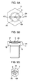
- FIG. 9A is a top view of a bolt top showing how to mount a small inlet in a concave portion on the bolt top.
- FIG. 9B is a cross sectional view taken on the arrow line X3-X3 in FIG. 9A.
- FIG. 9A shows the state before a sealant 17 is filled.
- an approximately cylindrical concave portion 25 is formed on the top of a bolt (metal object) 7 made of a conductive metal such as carbon steel or stainless steel, shoulders 26 are formed in the radial positions projected outside the concave portion 25 and opposed each other, and the connecting parts of the small inlet 3A are fixed in the shoulders 26 with a conductive adhesive 16. After that, the sealant 17 is filled in the concave portion 25 to make the top of the bolt 7 flat.
- the sealant 17 is an insulating material, and epoxy resin or low-temperature glass (hermetic seal) may be applied.
- the communication distance becomes longer.
- FIG. 9C is a top view of the top of the bolt when a bolt smaller in radius than the one shown in FIG. 9A is used.
- the small inlet 3A must be arranged so that the slit part corresponds to the radial center of the concave portion 25.
- Embedding the small inlet 3A in the concave portion 25 of the bolt 7 in this way with the sealant 17 filled therein allows the bolt 7 to work as an antenna to enable the communication with the IC chip 5 mounted in the embedded small inlet 3A.
- This structure prevents the small inlet 3A from being damaged because it is internally embedded.
- the bolt 7 in which the small inlet 3A is embedded can store quality management data on the goods, to which the bolt 7 is attached, in the IC chip 5 for use in managing the data.
- the bolt 7 itself can also be used as a screw-fixed RFIC tag.
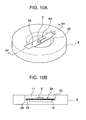
- FIG. 10A is a perspective view of a coin showing how to mount a small inlet in a concave portion of the coin.
- FIG. 10B is a cross sectional view taken on the arrow line X4-X4 in FIG. 10A.
- FIG. 10A shows the state before a sealant 17 is filled.
- an approximately cylindrical concave portion 25 is provided on one face of a coin (metal object) 8 made of conductive metal such as brass, cupronickel, and aluminum alloy, shoulders 26 are formed in the radial positions projected outwards and opposed each other, and the connecting parts of the small inlet 3A are fixed on the shoulders 26 with a conductive adhesive 16. After that, the sealant 17 is filled in the concave portion 25 to make the top of the one face of the coin 8 flat.
- the coin 8 in which the small inlet 3A is embedded can be used, for example, as a coin in a game hall.
- the game machine communicates with the IC chip 5 for reading/writing data.
- This machine updates or stores an increase/decrease in the customer's point in the IC chip 5, thus eliminating the need for the customer to carry many coins to the game hall for playing games there.
- Data stored in the game machines, on which the customer plays, can also be used for analyzing the trend.
- an insulating adhesive can also be used for mounting because the small inlet 3A is connected through electrostatic capacitory coupling via a base film not shown.
- the small inlet 3A is used in the first and second modifications of the second embodiment described above, it is also possible to flatten the thin metal plate 10A of the RFIC tag 1A in the first embodiment and to solder the connecting parts on the shoulder 26 of the concave portion 25 for mounting.
- the concave portion 25 on the bolt 7 or coin 8 it is also possible, after forming the concave portion 25 on the bolt 7 or coin 8, to infuse the sealant 17 from the bottom of the concave portion 25 to the top surface of the shoulder 26 to flatten the top surface, to form a connecting part on both the slit part and the shoulder 26 by printing a thin metal film (conductive thin film) using, for example, the ink jet method and, after that, to mount the IC chip 5 on the slit part to configure an RFIC tag. Finally, the sealant 17 is filled to the top end of the concave portion 25 to flatten the top end surface of the bolt 7 or coin 8.
- a thin metal film conductive thin film
- the slit forming an impedance matching circuit is formed as an L shape.
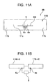
- the present invention is not limited to this shape but a T-shaped slit 6B shown in FIG. 11A may also be used.
- FIG. 11A is a top view of a small inlet 3B not including the IC chip 5 for easy understanding
- FIG. 11B is an equivalent circuit when the small inlet 3B is mounted on a metal member.
Landscapes
- Engineering & Computer Science (AREA)
- Microelectronics & Electronic Packaging (AREA)
- Computer Hardware Design (AREA)
- Physics & Mathematics (AREA)
- General Physics & Mathematics (AREA)
- Theoretical Computer Science (AREA)
- Electromagnetism (AREA)
- Computer Networks & Wireless Communication (AREA)
- Details Of Aerials (AREA)
- Die Bonding (AREA)
Applications Claiming Priority (1)
| Application Number | Priority Date | Filing Date | Title |
|---|---|---|---|
| JP2006305791A JP4950627B2 (ja) | 2006-11-10 | 2006-11-10 | Rficタグとその使用方法 |
Publications (3)
| Publication Number | Publication Date |
|---|---|
| EP1921570A2 true EP1921570A2 (fr) | 2008-05-14 |
| EP1921570A3 EP1921570A3 (fr) | 2010-03-31 |
| EP1921570B1 EP1921570B1 (fr) | 2012-02-22 |
Family
ID=38169721
Family Applications (1)
| Application Number | Title | Priority Date | Filing Date |
|---|---|---|---|
| EP07008137A Not-in-force EP1921570B1 (fr) | 2006-11-10 | 2007-04-20 | Étiquette de circuit intégré à fréquence radio et procédé d'utilisation de l'étiquette RFIC/RFID |
Country Status (6)
| Country | Link |
|---|---|
| US (1) | US7508347B2 (fr) |
| EP (1) | EP1921570B1 (fr) |
| JP (1) | JP4950627B2 (fr) |
| KR (1) | KR100848748B1 (fr) |
| CN (1) | CN101178783B (fr) |
| TW (1) | TWI332633B (fr) |
Cited By (8)
| Publication number | Priority date | Publication date | Assignee | Title |
|---|---|---|---|---|
| WO2009100729A1 (fr) * | 2008-02-12 | 2009-08-20 | Siemens Aktiengesellschaft | Marque d'identification pour identifier des objets à surface métallique |
| EP2453394A1 (fr) * | 2010-11-15 | 2012-05-16 | Neoid Limited | Etiquette RF avec structure de circuit résonant |
| EP2710569A4 (fr) * | 2011-05-17 | 2014-11-12 | Ndsu Res Foundation | Étiquettes rfid exemptes d'antenne discrète et appareil de transmission radio à circuit intégré |
| EP3140785A4 (fr) * | 2014-05-08 | 2017-12-13 | Tego Inc. | Étiquette d'identification par radiofréquence (rfid) souple destinée à être montée sur une surface métallique |
| CN108346854A (zh) * | 2018-02-06 | 2018-07-31 | 中国电子科技集团公司第三十八研究所 | 一种具有耦合馈电结构的天线 |
| EP3407262A1 (fr) * | 2017-05-24 | 2018-11-28 | SML Brand Identification Solutions Limited | Étiquette à configurations multiples |
| US10204244B2 (en) | 2014-09-30 | 2019-02-12 | Tego, Inc. | Data aggregating radio frequency tag |
| US10430702B2 (en) | 2005-12-09 | 2019-10-01 | Tego, Inc. | RF tag network connectivity through gateway facility |
Families Citing this family (34)
| Publication number | Priority date | Publication date | Assignee | Title |
|---|---|---|---|---|
| JP5027481B2 (ja) * | 2006-11-06 | 2012-09-19 | 株式会社日立製作所 | Icタグ |
| EP2178161A4 (fr) * | 2007-08-08 | 2010-12-22 | Fujitsu Ltd | Antenne à plaque pour étiquette et étiquette rfid employant cette antenne à plaque |
| USD588115S1 (en) * | 2007-08-20 | 2009-03-10 | Mitsumi Electric Co., Ltd | Antenna |
| WO2009142146A1 (fr) * | 2008-05-20 | 2009-11-26 | 東洋製罐株式会社 | Couvercle métallique doté d’une étiquette à circuit intégré et récipient métallique |
| US8710958B2 (en) * | 2008-07-10 | 2014-04-29 | Abbott Laboratories | Containers having radio frequency identification tags and method of applying radio frequency identification tags to containers |
| JP5114357B2 (ja) * | 2008-10-09 | 2013-01-09 | 株式会社日立製作所 | 無線icタグ |
| CN102273012B (zh) * | 2009-01-09 | 2013-11-20 | 株式会社村田制作所 | 无线ic器件及无线ic模块 |
| JP5358489B2 (ja) * | 2010-03-11 | 2013-12-04 | 株式会社日立製作所 | Rfidタグ及びその製造方法 |
| JP5521686B2 (ja) * | 2010-03-25 | 2014-06-18 | 株式会社村田製作所 | アンテナ装置及び無線通信デバイス |
| US9122967B2 (en) * | 2010-04-14 | 2015-09-01 | Technologies Roi, Llc | Radio frequency identification tags and methods employing ceramic components, which may be suitable for use in extreme environmental conditions |
| US8570224B2 (en) * | 2010-05-12 | 2013-10-29 | Qualcomm Incorporated | Apparatus providing thermal management for radio frequency devices |
| JP5527013B2 (ja) * | 2010-05-24 | 2014-06-18 | Tdk株式会社 | 近接型アンテナ及び無線通信機器 |
| USD635965S1 (en) * | 2010-11-15 | 2011-04-12 | Cheng Uei Precision Industry Co., Ltd. | Antenna |
| DE102011104170A1 (de) * | 2011-06-14 | 2012-12-20 | Schreiner Group Gmbh & Co. Kg | Transponderetikett und Herstellungsverfahren für ein Transponderetikett |
| JP5777096B2 (ja) | 2011-07-21 | 2015-09-09 | 株式会社スマート | 万能icタグとその製造法、及び通信管理システム |
| US8477076B1 (en) * | 2012-01-25 | 2013-07-02 | Clearcount Medical Solutions, Inc. | Antenna coupler mechanism |
| US9515376B2 (en) | 2012-01-25 | 2016-12-06 | Stryker Combo, L.L.C. | Antenna coupler mechanism |
| US8477077B1 (en) * | 2012-01-25 | 2013-07-02 | Clearcount Medical Solutions, Inc. | Antenna coupler mechanism systems and methods |
| TWI462023B (zh) * | 2012-02-08 | 2014-11-21 | Favite Inc | 可耦合金屬的電子標籤(tag) |
| JP6019211B2 (ja) * | 2012-03-21 | 2016-11-02 | 熊光 蔡 | ビジョンインタフェース装置及びデータ伝送システム |
| USD704169S1 (en) * | 2012-09-26 | 2014-05-06 | Avery Dennison Corporation | RFID antenna |
| US9172130B2 (en) * | 2013-03-13 | 2015-10-27 | Avery Dennison Corporation | RFID inlay incorporating a ground plane |
| USD717282S1 (en) * | 2014-04-15 | 2014-11-11 | Avery Dennison Corporation | Antenna |
| CN106134000B (zh) * | 2014-04-28 | 2019-04-02 | 株式会社村田制作所 | 无线ic器件、夹状rfid标签以及附带rfid标签的物品 |
| GB2536334B (en) | 2015-01-26 | 2017-08-23 | Neoid Ltd (Shenzhen) | RF tag with resonant circuit structure |
| JP6560610B2 (ja) * | 2015-12-18 | 2019-08-14 | 株式会社ジャパンディスプレイ | 表示装置 |
| US10320054B2 (en) * | 2016-10-28 | 2019-06-11 | Avery Dennison Retail Information Services, Llc | RFID tags designed to work on difficult substrates |
| EP3340427A1 (fr) * | 2016-12-22 | 2018-06-27 | Jae Beom Kim | Cadre métallique transmettant les ondes électromagnétiques ou ayant la fonction de rayonnement thermique |
| CN211655071U (zh) * | 2017-10-20 | 2020-10-09 | 株式会社村田制作所 | 卡式无线通信设备 |
| DE102018106432A1 (de) * | 2018-03-20 | 2019-09-26 | Erich Utsch Ag | Anordnung aus einem Schild und einem das Schild tragenden Schildträger |
| WO2020059154A1 (fr) * | 2018-09-21 | 2020-03-26 | ヨメテル株式会社 | Substrat de communication sans fil et étiquette de communication sans fil |
| US10840964B2 (en) * | 2018-10-16 | 2020-11-17 | Murata Manufacturing Co., Ltd. | Smartphone case |
| WO2021044930A1 (fr) * | 2019-09-05 | 2021-03-11 | 株式会社村田製作所 | Dispositif médical métallique à étiquette à circuit intégré sans fil |
| DE102021123104A1 (de) * | 2021-09-07 | 2023-03-09 | Schreiner Group Gmbh & Co. Kg | Etikett mit Aufstellmechanismus |
Citations (4)
| Publication number | Priority date | Publication date | Assignee | Title |
|---|---|---|---|---|
| EP1548639A1 (fr) | 2003-12-25 | 2005-06-29 | Hitachi, Ltd. | Etiquette IC sans fil d'IC, et méthode et appareil pour fabriquer la même |
| JP2005309811A (ja) | 2004-04-22 | 2005-11-04 | Mitsubishi Materials Corp | Rfidタグ及びrfidシステム |
| US20060028344A1 (en) | 2003-04-25 | 2006-02-09 | Forster Ian J | Extended range RFID system |
| US20060145872A1 (en) | 2004-12-16 | 2006-07-06 | Denso Corporation | IC tag and IC tag attachment structure |
Family Cites Families (8)
| Publication number | Priority date | Publication date | Assignee | Title |
|---|---|---|---|---|
| FR2779255B1 (fr) * | 1998-05-27 | 2001-10-12 | Gemplus Card Int | Procede de fabrication d'un dispositif electronique portable comportant au moins une puce de circuit integre |
| JP2003110345A (ja) * | 2001-09-27 | 2003-04-11 | Hitachi Ltd | アンテナ素子及びそれを用いた通信機 |
| JP4177241B2 (ja) * | 2003-12-04 | 2008-11-05 | 株式会社日立情報制御ソリューションズ | 無線icタグ用アンテナ、無線icタグ及び無線icタグ付き容器 |
| JP4348282B2 (ja) * | 2004-06-11 | 2009-10-21 | 株式会社日立製作所 | 無線用icタグ、及び無線用icタグの製造方法 |
| KR100847351B1 (ko) * | 2004-11-25 | 2008-07-21 | 주식회사 손텍 | 무선주파수식별표지 |
| JP2006311372A (ja) * | 2005-04-28 | 2006-11-09 | Hitachi Ltd | 無線icタグ |
| JP4075919B2 (ja) * | 2005-09-29 | 2008-04-16 | オムロン株式会社 | アンテナユニットおよび非接触icタグ |
| JP4854362B2 (ja) * | 2006-03-30 | 2012-01-18 | 富士通株式会社 | Rfidタグ及びその製造方法 |
-
2006
- 2006-11-10 JP JP2006305791A patent/JP4950627B2/ja not_active Expired - Fee Related
-
2007
- 2007-04-20 EP EP07008137A patent/EP1921570B1/fr not_active Not-in-force
- 2007-04-26 TW TW096114820A patent/TWI332633B/zh not_active IP Right Cessation
- 2007-04-27 US US11/741,003 patent/US7508347B2/en not_active Expired - Fee Related
- 2007-06-14 KR KR1020070058374A patent/KR100848748B1/ko not_active Expired - Fee Related
- 2007-06-15 CN CN2007101067009A patent/CN101178783B/zh not_active Expired - Fee Related
Patent Citations (4)
| Publication number | Priority date | Publication date | Assignee | Title |
|---|---|---|---|---|
| US20060028344A1 (en) | 2003-04-25 | 2006-02-09 | Forster Ian J | Extended range RFID system |
| EP1548639A1 (fr) | 2003-12-25 | 2005-06-29 | Hitachi, Ltd. | Etiquette IC sans fil d'IC, et méthode et appareil pour fabriquer la même |
| JP2005309811A (ja) | 2004-04-22 | 2005-11-04 | Mitsubishi Materials Corp | Rfidタグ及びrfidシステム |
| US20060145872A1 (en) | 2004-12-16 | 2006-07-06 | Denso Corporation | IC tag and IC tag attachment structure |
Cited By (12)
| Publication number | Priority date | Publication date | Assignee | Title |
|---|---|---|---|---|
| US10430702B2 (en) | 2005-12-09 | 2019-10-01 | Tego, Inc. | RF tag network connectivity through gateway facility |
| US10691992B2 (en) | 2005-12-09 | 2020-06-23 | Tego, Inc. | RF tag with memory management |
| WO2009100729A1 (fr) * | 2008-02-12 | 2009-08-20 | Siemens Aktiengesellschaft | Marque d'identification pour identifier des objets à surface métallique |
| EP2453394A1 (fr) * | 2010-11-15 | 2012-05-16 | Neoid Limited | Etiquette RF avec structure de circuit résonant |
| EP2710569A4 (fr) * | 2011-05-17 | 2014-11-12 | Ndsu Res Foundation | Étiquettes rfid exemptes d'antenne discrète et appareil de transmission radio à circuit intégré |
| EP3140785A4 (fr) * | 2014-05-08 | 2017-12-13 | Tego Inc. | Étiquette d'identification par radiofréquence (rfid) souple destinée à être montée sur une surface métallique |
| US10204244B2 (en) | 2014-09-30 | 2019-02-12 | Tego, Inc. | Data aggregating radio frequency tag |
| US10445536B2 (en) | 2014-09-30 | 2019-10-15 | Tego, Inc. | Operating system for an RF tag |
| US10891449B2 (en) | 2014-09-30 | 2021-01-12 | Tego, Inc. | Self-monitoring wireless computing device |
| EP3407262A1 (fr) * | 2017-05-24 | 2018-11-28 | SML Brand Identification Solutions Limited | Étiquette à configurations multiples |
| CN108346854A (zh) * | 2018-02-06 | 2018-07-31 | 中国电子科技集团公司第三十八研究所 | 一种具有耦合馈电结构的天线 |
| CN108346854B (zh) * | 2018-02-06 | 2020-09-08 | 中国电子科技集团公司第三十八研究所 | 一种具有耦合馈电结构的天线 |
Also Published As
| Publication number | Publication date |
|---|---|
| CN101178783B (zh) | 2010-06-02 |
| US7508347B2 (en) | 2009-03-24 |
| TWI332633B (en) | 2010-11-01 |
| JP4950627B2 (ja) | 2012-06-13 |
| KR20080042660A (ko) | 2008-05-15 |
| EP1921570A3 (fr) | 2010-03-31 |
| TW200821949A (en) | 2008-05-16 |
| US20080111760A1 (en) | 2008-05-15 |
| KR100848748B1 (ko) | 2008-07-25 |
| JP2008123222A (ja) | 2008-05-29 |
| CN101178783A (zh) | 2008-05-14 |
| EP1921570B1 (fr) | 2012-02-22 |
Similar Documents
| Publication | Publication Date | Title |
|---|---|---|
| EP1921570B1 (fr) | Étiquette de circuit intégré à fréquence radio et procédé d'utilisation de l'étiquette RFIC/RFID | |
| US7126482B2 (en) | RFID tag and its manufacturing method | |
| JP5278611B2 (ja) | 通信システム、情報記録媒体、中継通信装置 | |
| EP3367500B1 (fr) | Dispositif ci sans fil | |
| TWI384403B (zh) | Radio frequency identification tag, manufacturing method of radio frequency identification tag, and setting method of radio frequency identification tag | |
| EP1884889A2 (fr) | Dispositif semi-conducteur | |
| US20080150725A1 (en) | Rfid label tag and method of manufacturing the same | |
| JPH11509024A (ja) | カードまたはラベル用の非接触電子モジュール | |
| CN107430701A (zh) | Rf标签 | |
| US7268417B2 (en) | Card-type circuit device | |
| WO2018092897A1 (fr) | Carte à double circuit intégré à couplage électromagnétique et module de circuit intégré | |
| US10804594B2 (en) | Single-face antenna module comprising CMS device | |
| US8669910B2 (en) | Antenna arrangement for a chip card | |
| KR20090043077A (ko) | 알에프아이디 안테나 및 그 제조방법 | |
| JP5187083B2 (ja) | Rfidタグ、rfidシステム及びrfidタグ製造方法 | |
| JP4873158B2 (ja) | Rfidリーダ装置 | |
| KR20050120481A (ko) | 전자 무선 인식 장치 및 전자 무선 인식 장치의 제조방법 | |
| KR100735618B1 (ko) | 알에프아이디 안테나 및 그 제조방법 | |
| JP2006301533A (ja) | 表示装置およびその製造方法 | |
| JP5594178B2 (ja) | 通信システム | |
| JP5195241B2 (ja) | 耐熱性icタグストラップ | |
| KR20080103811A (ko) | 알에프아이디 안테나의 제조방법 | |
| WO2024095749A1 (fr) | Corps de logement de composant électronique, et composant électronique accueillant un matériau de conditionnement de corps | |
| KR100973286B1 (ko) | 스마트 카드 접촉 단자 및 이를 이용한 스마트 카드 | |
| JP4775292B2 (ja) | 無線icデバイス及びその製造方法 |
Legal Events
| Date | Code | Title | Description |
|---|---|---|---|
| PUAI | Public reference made under article 153(3) epc to a published international application that has entered the european phase |
Free format text: ORIGINAL CODE: 0009012 |
|
| 17P | Request for examination filed |
Effective date: 20080331 |
|
| AK | Designated contracting states |
Kind code of ref document: A2 Designated state(s): AT BE BG CH CY CZ DE DK EE ES FI FR GB GR HU IE IS IT LI LT LU LV MC MT NL PL PT RO SE SI SK TR |
|
| AX | Request for extension of the european patent |
Extension state: AL BA HR MK RS |
|
| PUAL | Search report despatched |
Free format text: ORIGINAL CODE: 0009013 |
|
| AK | Designated contracting states |
Kind code of ref document: A3 Designated state(s): AT BE BG CH CY CZ DE DK EE ES FI FR GB GR HU IE IS IT LI LT LU LV MC MT NL PL PT RO SE SI SK TR |
|
| AX | Request for extension of the european patent |
Extension state: AL BA HR MK RS |
|
| 17Q | First examination report despatched |
Effective date: 20100625 |
|
| AKX | Designation fees paid |
Designated state(s): DE FR GB |
|
| GRAP | Despatch of communication of intention to grant a patent |
Free format text: ORIGINAL CODE: EPIDOSNIGR1 |
|
| GRAS | Grant fee paid |
Free format text: ORIGINAL CODE: EPIDOSNIGR3 |
|
| GRAA | (expected) grant |
Free format text: ORIGINAL CODE: 0009210 |
|
| AK | Designated contracting states |
Kind code of ref document: B1 Designated state(s): DE FR GB |
|
| REG | Reference to a national code |
Ref country code: GB Ref legal event code: FG4D |
|
| REG | Reference to a national code |
Ref country code: DE Ref legal event code: R096 Ref document number: 602007020789 Country of ref document: DE Effective date: 20120419 |
|
| PLBE | No opposition filed within time limit |
Free format text: ORIGINAL CODE: 0009261 |
|
| STAA | Information on the status of an ep patent application or granted ep patent |
Free format text: STATUS: NO OPPOSITION FILED WITHIN TIME LIMIT |
|
| 26N | No opposition filed |
Effective date: 20121123 |
|
| REG | Reference to a national code |
Ref country code: DE Ref legal event code: R097 Ref document number: 602007020789 Country of ref document: DE Effective date: 20121123 |
|
| PGFP | Annual fee paid to national office [announced via postgrant information from national office to epo] |
Ref country code: DE Payment date: 20130508 Year of fee payment: 7 Ref country code: GB Payment date: 20130417 Year of fee payment: 7 |
|
| PGFP | Annual fee paid to national office [announced via postgrant information from national office to epo] |
Ref country code: FR Payment date: 20130625 Year of fee payment: 7 |
|
| REG | Reference to a national code |
Ref country code: DE Ref legal event code: R119 Ref document number: 602007020789 Country of ref document: DE |
|
| GBPC | Gb: european patent ceased through non-payment of renewal fee |
Effective date: 20140420 |
|
| REG | Reference to a national code |
Ref country code: DE Ref legal event code: R119 Ref document number: 602007020789 Country of ref document: DE Effective date: 20141101 |
|
| REG | Reference to a national code |
Ref country code: FR Ref legal event code: ST Effective date: 20141231 |
|
| PG25 | Lapsed in a contracting state [announced via postgrant information from national office to epo] |
Ref country code: GB Free format text: LAPSE BECAUSE OF NON-PAYMENT OF DUE FEES Effective date: 20140420 Ref country code: DE Free format text: LAPSE BECAUSE OF NON-PAYMENT OF DUE FEES Effective date: 20141101 |
|
| PG25 | Lapsed in a contracting state [announced via postgrant information from national office to epo] |
Ref country code: FR Free format text: LAPSE BECAUSE OF NON-PAYMENT OF DUE FEES Effective date: 20140430 |