EP1921643A2 - Matrice de contact par pression - Google Patents
Matrice de contact par pression Download PDFInfo
- Publication number
- EP1921643A2 EP1921643A2 EP07018492A EP07018492A EP1921643A2 EP 1921643 A2 EP1921643 A2 EP 1921643A2 EP 07018492 A EP07018492 A EP 07018492A EP 07018492 A EP07018492 A EP 07018492A EP 1921643 A2 EP1921643 A2 EP 1921643A2
- Authority
- EP
- European Patent Office
- Prior art keywords
- pad
- terminal contact
- contact arrangement
- pad elements
- arrangement according
- Prior art date
- Legal status (The legal status is an assumption and is not a legal conclusion. Google has not performed a legal analysis and makes no representation as to the accuracy of the status listed.)
- Granted
Links
Images


Classifications
-
- H—ELECTRICITY
- H05—ELECTRIC TECHNIQUES NOT OTHERWISE PROVIDED FOR
- H05K—PRINTED CIRCUITS; CASINGS OR CONSTRUCTIONAL DETAILS OF ELECTRIC APPARATUS; MANUFACTURE OF ASSEMBLAGES OF ELECTRICAL COMPONENTS
- H05K3/00—Apparatus or processes for manufacturing printed circuits
- H05K3/40—Forming printed elements for providing electric connections to or between printed circuits
- H05K3/4007—Surface contacts, e.g. bumps
- H05K3/4015—Surface contacts, e.g. bumps using auxiliary conductive elements, e.g. pieces of metal foil, metallic spheres
-
- H—ELECTRICITY
- H01—ELECTRIC ELEMENTS
- H01R—ELECTRICALLY-CONDUCTIVE CONNECTIONS; STRUCTURAL ASSOCIATIONS OF A PLURALITY OF MUTUALLY-INSULATED ELECTRICAL CONNECTING ELEMENTS; COUPLING DEVICES; CURRENT COLLECTORS
- H01R12/00—Structural associations of a plurality of mutually-insulated electrical connecting elements, specially adapted for printed circuits, e.g. printed circuit boards [PCB], flat or ribbon cables, or like generally planar structures, e.g. terminal strips, terminal blocks; Coupling devices specially adapted for printed circuits, flat or ribbon cables, or like generally planar structures; Terminals specially adapted for contact with, or insertion into, printed circuits, flat or ribbon cables, or like generally planar structures
- H01R12/50—Fixed connections
- H01R12/51—Fixed connections for rigid printed circuits or like structures
- H01R12/55—Fixed connections for rigid printed circuits or like structures characterised by the terminals
- H01R12/57—Fixed connections for rigid printed circuits or like structures characterised by the terminals surface mounting terminals
-
- H—ELECTRICITY
- H01—ELECTRIC ELEMENTS
- H01R—ELECTRICALLY-CONDUCTIVE CONNECTIONS; STRUCTURAL ASSOCIATIONS OF A PLURALITY OF MUTUALLY-INSULATED ELECTRICAL CONNECTING ELEMENTS; COUPLING DEVICES; CURRENT COLLECTORS
- H01R43/00—Apparatus or processes specially adapted for manufacturing, assembling, maintaining, or repairing of line connectors or current collectors or for joining electric conductors
- H01R43/16—Apparatus or processes specially adapted for manufacturing, assembling, maintaining, or repairing of line connectors or current collectors or for joining electric conductors for manufacturing contact members, e.g. by punching and by bending
-
- H—ELECTRICITY
- H01—ELECTRIC ELEMENTS
- H01H—ELECTRIC SWITCHES; RELAYS; SELECTORS; EMERGENCY PROTECTIVE DEVICES
- H01H13/00—Switches having rectilinearly-movable operating part or parts adapted for pushing or pulling in one direction only, e.g. push-button switch
- H01H13/70—Switches having rectilinearly-movable operating part or parts adapted for pushing or pulling in one direction only, e.g. push-button switch having a plurality of operating members associated with different sets of contacts, e.g. keyboard
- H01H13/81—Switches having rectilinearly-movable operating part or parts adapted for pushing or pulling in one direction only, e.g. push-button switch having a plurality of operating members associated with different sets of contacts, e.g. keyboard characterised by electrical connections to external devices
-
- H—ELECTRICITY
- H05—ELECTRIC TECHNIQUES NOT OTHERWISE PROVIDED FOR
- H05K—PRINTED CIRCUITS; CASINGS OR CONSTRUCTIONAL DETAILS OF ELECTRIC APPARATUS; MANUFACTURE OF ASSEMBLAGES OF ELECTRICAL COMPONENTS
- H05K1/00—Printed circuits
- H05K1/02—Details
- H05K1/11—Printed elements for providing electric connections to or between printed circuits
-
- H—ELECTRICITY
- H05—ELECTRIC TECHNIQUES NOT OTHERWISE PROVIDED FOR
- H05K—PRINTED CIRCUITS; CASINGS OR CONSTRUCTIONAL DETAILS OF ELECTRIC APPARATUS; MANUFACTURE OF ASSEMBLAGES OF ELECTRICAL COMPONENTS
- H05K2201/00—Indexing scheme relating to printed circuits covered by H05K1/00
- H05K2201/10—Details of components or other objects attached to or integrated in a printed circuit board
- H05K2201/10007—Types of components
- H05K2201/10053—Switch
-
- H—ELECTRICITY
- H05—ELECTRIC TECHNIQUES NOT OTHERWISE PROVIDED FOR
- H05K—PRINTED CIRCUITS; CASINGS OR CONSTRUCTIONAL DETAILS OF ELECTRIC APPARATUS; MANUFACTURE OF ASSEMBLAGES OF ELECTRICAL COMPONENTS
- H05K2203/00—Indexing scheme relating to apparatus or processes for manufacturing printed circuits covered by H05K3/00
- H05K2203/03—Metal processing
- H05K2203/033—Punching metal foil, e.g. solder foil
-
- H—ELECTRICITY
- H05—ELECTRIC TECHNIQUES NOT OTHERWISE PROVIDED FOR
- H05K—PRINTED CIRCUITS; CASINGS OR CONSTRUCTIONAL DETAILS OF ELECTRIC APPARATUS; MANUFACTURE OF ASSEMBLAGES OF ELECTRICAL COMPONENTS
- H05K3/00—Apparatus or processes for manufacturing printed circuits
- H05K3/30—Assembling printed circuits with electric components, e.g. with resistors
- H05K3/32—Assembling printed circuits with electric components, e.g. with resistors electrically connecting electric components or wires to printed circuits
- H05K3/34—Assembling printed circuits with electric components, e.g. with resistors electrically connecting electric components or wires to printed circuits by soldering
- H05K3/341—Surface mounted components
Definitions
- the invention relates in particular to a contact-contact array or a AnpressCAMan angel, in particular SMD-solderable.
- the invention further relates to a method for attaching AnpressCAMen to a circuit board and in particular by means of a AnpressCAMan nie.
- the invention relates generally to a terminal contact arrangement.
- Printed circuit boards have contact surfaces, in particular for connection purposes, on which, for example, components can be soldered. These contact surfaces are often referred to as pad surfaces or shortly as pads. Hereinafter, these pads, after being on the circuit board, will be referred to as board pads.
- the positioning is made with respect to the circuit board pads and then initiated the soldering process. Because the pad elements fastened to the pilot strip are fixed to one another or to one another, they do not lose their exact positioning.
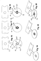
- Fig. 1 is a schematic plan view of a surface of a circuit board 10, on which circuit board pads 11 are formed, for example, have a circular surface shape.
- an annular printed circuit board pad 12 is shown, which surrounds a circular printed circuit board pad 13 spaced.
- segmental printed circuit board pads 14, 15, 16 and 17 are shown. Conductor tracks are designated by 18.
- pad elements 140, 150, 160, 170 may be referred to as pad elements 140, 150, 160, 170.
- FIG. 3 shows a pilot strip 25 to which four pad elements 141, 151, 161, 171 of the pressing contact arrangement 21 are fastened by means of a web 26.
- FIGS. 3 and 4 illustrate a first manufacturing stage of the solderable contact pressing arrangement 21 shown in FIGS. 7 and 8. A plurality of such contact contact arrangements 21 may be arranged at a distance from the pilot strip 25. The individual pad elements 141, 151, 161, 171 are separated by punched slots 28 and connected in this first production stage by a circular disk 27.
- a molding material 130 is introduced into the slots 28.
- the molding material 130 preferably connects the pad elements 141, 151, 161, 171 to one another at the edges.
- the pad elements 141, 151, 161, 171 form, after in a third Endstanzgrin punching out of a hole 29 leaving disc 27 (an unnecessary connecting part), a unit.
- the finished Anpressromean angel 21 shown in Fig. 7 and 8 can then be easily aligned with the PCB contact pads 14, 15, 16, 17 and soldered. After soldering takes place in a further step, the separation of the web 26, preferably along a predetermined breaking point or predetermined breaking line.
- non-segment-shaped pad elements are formed, but square pad elements 142, 152, 162 and 172. These are shown in FIGS. 9 and 10 separated by slots 30, but centrally with a cross-shaped Disc 31 connected, which - as seen in Fig. 13 - leaves after punching out a cross-shaped hole 32.
- Two webs 26 each connect the pad elements 162, 172 to the pilot strip 25, predetermined breaking points 60 are, as shown, provided.
- a molding material 130 is injected into the slots 30 before punching out the disk 31, and thus the pad members 142, 152, 162, 172 are connected to each other and remain connected even after the cross-shaped disk 31 is punched out.
- the pressing contact assembly 22 thus formed is placed and soldered on respective circuit board pads.
- the Anpresstitlean angel (generally: terminal contact arrangement) 23, a first pad member 143 in the form of an annular contact disc and a second pad member 153 in the Shape of a contact plate on.
- two slits 34 and 35 are punched in a circular, preferably made of metal disc 33 in mirror image. These slots 34, 35 form the contour for the second or inner pad member 153, i. a first pressing contact in the form of a circular plate. However, according to FIG. 15, this second pad element 153 (pressing contact) is still connected by connecting webs 36, 37 to the first, outer annular pad element 143 (pressing contact).
- the slots 34, 35 are filled with molding material 130 and subsequently in a third method step, two circular disks (non-required connecting parts) are punched out, whose diameter holes 38 and 39 according to FIGS. 19 and 20 equivalent.
- the first and second pad elements 143, 153 are electrically isolated but mechanically connected:
- the inner pad element 153 is galvanically separated from the outer pad element 143, but remains mechanically connected to one another by means of the molding compound 200, 201 with the aid of the molding material 130.
- predetermined breaking points 60 are provided in the joints (i.e., lands 26) between the pilot strips 25 and at least one of the pad members 171; 162; 172; 253 predetermined breaking points 60 are provided.
- the invention relates in particular to an arrangement of pressing contacts, wherein the pressing contacts are formed by so-called pad elements which, when it comes to pressing contacts, have pressing contact zones in which the contact pressure takes place.
- terminal contacts can also be provided in terminal contact arrangements in order to be soldered to printed circuit board pads as long as they still form a unit.
- the pad elements are used as pressing contacts, then it may be expedient to provide a galvanic coating in the Anpress1:00zonen the pad elements.
- the pad elements forming a terminal contact or pressing contact arrangement are preferably connected to one another in a coplanar plane.
- the pad elements forming a terminal contact or AnpressANDan angel are punched from a surface element, such as a metal sheet, wherein preferably slots or recesses delimit the pad elements from each other. After punching out the recesses forming sheet metal or surface element parts, the slots or recesses formed are completely or partially filled by the molding material 130, which produces a stable mechanical connection between the different pad elements, but also the pad elements electrically insulated from each other.
Landscapes
- Engineering & Computer Science (AREA)
- Manufacturing & Machinery (AREA)
- Microelectronics & Electronic Packaging (AREA)
- Coupling Device And Connection With Printed Circuit (AREA)
- Multi-Conductor Connections (AREA)
Applications Claiming Priority (1)
| Application Number | Priority Date | Filing Date | Title |
|---|---|---|---|
| DE102006052462A DE102006052462A1 (de) | 2006-11-07 | 2006-11-07 | Anpress-Kontakt-Array |
Publications (3)
| Publication Number | Publication Date |
|---|---|
| EP1921643A2 true EP1921643A2 (fr) | 2008-05-14 |
| EP1921643A3 EP1921643A3 (fr) | 2008-08-06 |
| EP1921643B1 EP1921643B1 (fr) | 2012-05-02 |
Family
ID=38965350
Family Applications (1)
| Application Number | Title | Priority Date | Filing Date |
|---|---|---|---|
| EP07018492A Not-in-force EP1921643B1 (fr) | 2006-11-07 | 2007-09-20 | Matrice de contact par pression |
Country Status (3)
| Country | Link |
|---|---|
| EP (1) | EP1921643B1 (fr) |
| AT (1) | ATE556420T1 (fr) |
| DE (1) | DE102006052462A1 (fr) |
Families Citing this family (1)
| Publication number | Priority date | Publication date | Assignee | Title |
|---|---|---|---|---|
| CN108770196A (zh) * | 2018-04-24 | 2018-11-06 | 深圳市比亚迪电子部品件有限公司 | 一种防止柔性线路板焊盘脱落结构 |
Family Cites Families (4)
| Publication number | Priority date | Publication date | Assignee | Title |
|---|---|---|---|---|
| DE4301928A1 (de) * | 1993-01-25 | 1994-07-28 | Siemens Nixdorf Inf Syst | Leitlack-Kontaktfläche |
| JPH07335679A (ja) * | 1994-06-03 | 1995-12-22 | Fujitsu Ten Ltd | アルミポストのはんだ付け構造 |
| US5791911A (en) * | 1996-10-25 | 1998-08-11 | International Business Machines Corporation | Coaxial interconnect devices and methods of making the same |
| TW380358B (en) * | 1996-12-10 | 2000-01-21 | Whitaker Corp | Surface mount pad |
-
2006
- 2006-11-07 DE DE102006052462A patent/DE102006052462A1/de not_active Withdrawn
-
2007
- 2007-09-20 EP EP07018492A patent/EP1921643B1/fr not_active Not-in-force
- 2007-09-20 AT AT07018492T patent/ATE556420T1/de active
Also Published As
| Publication number | Publication date |
|---|---|
| ATE556420T1 (de) | 2012-05-15 |
| EP1921643B1 (fr) | 2012-05-02 |
| EP1921643A3 (fr) | 2008-08-06 |
| DE102006052462A1 (de) | 2008-05-08 |
Similar Documents
| Publication | Publication Date | Title |
|---|---|---|
| DE69634005T2 (de) | Steckverbinder mit integriertem leiterplattenzusammenbau | |
| DE102008005547B4 (de) | Leistungshalbleitermodul und Schaltungsanordnung mit einem Leistungshalbleitermodul | |
| DE3011068C2 (de) | Verfahren zur Herstellung einer Gegenplatte mit elektrisch voneinander isolierten Potential- und Masseplatten | |
| DE102006011657A1 (de) | Kontaktstift und Verfahren zu dessen Herstellung | |
| DE102005041058A1 (de) | Verfahren zur Herstellung einer mehrschichtigen Karte | |
| DE19809138A1 (de) | Leiterplatte mit SMD-Bauelementen | |
| WO2009089981A1 (fr) | Contact à emmancher avec un socle, une broche de contact et une deuxième broche | |
| DE68916766T2 (de) | Stift mit rohrförmigem, elliptischem, nachgiebigem Teil und Verfahren zum Anbringen in entsprechender Hülse. | |
| DE19735409A1 (de) | Leiterplatine sowie zugehöriges Kontaktelement | |
| DE69402049T2 (de) | Leiterplatte mit elektrischem Adaptorstift und dessen Herstellungsverfahren. | |
| DE102014208101A1 (de) | Elektrische Verbindungsanordnung für die elektrische Verbindung von Leiterplatten untereinander mittels lötfreier Einpresskontaktierung | |
| DE10245688A1 (de) | Mehrschichtkeramikelektronikteil, Elektronikteilaggregat und Verfahren zum Herstellen eines Mehrschichtkeramikelektronikteils | |
| DE3010876A1 (de) | Verfahren zur herstellung einer leiterplatte | |
| WO2005032224A1 (fr) | Carte de circuits imprimes comprenant un dispositif de maintien concu pour maintenir des composants electroniques cables, procede pour produire une telle carte de circuits imprimes et son utilisation dans un four a braser | |
| DE2619658A1 (de) | Verfahren zum herstellen einer elektrischen verbindereinheit | |
| DE102020100364B4 (de) | Leistungselektronische Baugruppe mit einem Substrat, einer Hülse und einem Kontaktstift und Verfahren zur Herstellung einer solchen Baugruppe | |
| EP0765110B1 (fr) | Plaquette de circuit et son procédé de fabrication | |
| DE60212299T2 (de) | Pin-grid-array elektrischer Steckverbinder | |
| DE102010039204A1 (de) | Elektrische Kontaktierung | |
| DE3801352C2 (fr) | ||
| DE2812976C2 (de) | Verfahren zur Feststellung des Versatzes zwischen Leiterbahnen und Kontaktlöchern bei einer Leiterplatte sowie eine Leiterplatte zur Verwendung in diesem Verfahren | |
| EP1921643B1 (fr) | Matrice de contact par pression | |
| EP0995235B1 (fr) | Contact pour de minuscules contacts de liaison et procede de production d'un contact | |
| DE102014117536B4 (de) | Verfahren zur seitlichen Verbindung zweier Leiterplatten und optoelektronischer Sensor mit zwei im Winkel verbundenen Leiterplatten | |
| DE102019132852B4 (de) | Verfahren zum Herstellen eines Leiterstrukturelements und Leiterstrukturelement |
Legal Events
| Date | Code | Title | Description |
|---|---|---|---|
| PUAI | Public reference made under article 153(3) epc to a published international application that has entered the european phase |
Free format text: ORIGINAL CODE: 0009012 |
|
| AK | Designated contracting states |
Kind code of ref document: A2 Designated state(s): AT BE BG CH CY CZ DE DK EE ES FI FR GB GR HU IE IS IT LI LT LU LV MC MT NL PL PT RO SE SI SK TR |
|
| AX | Request for extension of the european patent |
Extension state: AL BA HR MK RS |
|
| PUAL | Search report despatched |
Free format text: ORIGINAL CODE: 0009013 |
|
| AK | Designated contracting states |
Kind code of ref document: A3 Designated state(s): AT BE BG CH CY CZ DE DK EE ES FI FR GB GR HU IE IS IT LI LT LU LV MC MT NL PL PT RO SE SI SK TR |
|
| AX | Request for extension of the european patent |
Extension state: AL BA HR MK RS |
|
| RIC1 | Information provided on ipc code assigned before grant |
Ipc: H05K 3/40 20060101ALI20080627BHEP Ipc: H01H 13/81 20060101AFI20080201BHEP |
|
| 17P | Request for examination filed |
Effective date: 20081218 |
|
| AKX | Designation fees paid |
Designated state(s): AT BE BG CH CY CZ DE DK EE ES FI FR GB GR HU IE IS IT LI LT LU LV MC MT NL PL PT RO SE SI SK TR |
|
| GRAP | Despatch of communication of intention to grant a patent |
Free format text: ORIGINAL CODE: EPIDOSNIGR1 |
|
| GRAS | Grant fee paid |
Free format text: ORIGINAL CODE: EPIDOSNIGR3 |
|
| GRAA | (expected) grant |
Free format text: ORIGINAL CODE: 0009210 |
|
| AK | Designated contracting states |
Kind code of ref document: B1 Designated state(s): AT BE BG CH CY CZ DE DK EE ES FI FR GB GR HU IE IS IT LI LT LU LV MC MT NL PL PT RO SE SI SK TR |
|
| REG | Reference to a national code |
Ref country code: GB Ref legal event code: FG4D Free format text: NOT ENGLISH |
|
| REG | Reference to a national code |
Ref country code: AT Ref legal event code: REF Ref document number: 556420 Country of ref document: AT Kind code of ref document: T Effective date: 20120515 Ref country code: CH Ref legal event code: EP |
|
| REG | Reference to a national code |
Ref country code: IE Ref legal event code: FG4D Free format text: LANGUAGE OF EP DOCUMENT: GERMAN |
|
| REG | Reference to a national code |
Ref country code: DE Ref legal event code: R096 Ref document number: 502007009803 Country of ref document: DE Effective date: 20120705 |
|
| REG | Reference to a national code |
Ref country code: NL Ref legal event code: VDEP Effective date: 20120502 |
|
| REG | Reference to a national code |
Ref country code: LT Ref legal event code: MG4D Effective date: 20120502 |
|
| PG25 | Lapsed in a contracting state [announced via postgrant information from national office to epo] |
Ref country code: CY Free format text: LAPSE BECAUSE OF FAILURE TO SUBMIT A TRANSLATION OF THE DESCRIPTION OR TO PAY THE FEE WITHIN THE PRESCRIBED TIME-LIMIT Effective date: 20120502 Ref country code: LT Free format text: LAPSE BECAUSE OF FAILURE TO SUBMIT A TRANSLATION OF THE DESCRIPTION OR TO PAY THE FEE WITHIN THE PRESCRIBED TIME-LIMIT Effective date: 20120502 Ref country code: IS Free format text: LAPSE BECAUSE OF FAILURE TO SUBMIT A TRANSLATION OF THE DESCRIPTION OR TO PAY THE FEE WITHIN THE PRESCRIBED TIME-LIMIT Effective date: 20120902 Ref country code: PL Free format text: LAPSE BECAUSE OF FAILURE TO SUBMIT A TRANSLATION OF THE DESCRIPTION OR TO PAY THE FEE WITHIN THE PRESCRIBED TIME-LIMIT Effective date: 20120502 Ref country code: SE Free format text: LAPSE BECAUSE OF FAILURE TO SUBMIT A TRANSLATION OF THE DESCRIPTION OR TO PAY THE FEE WITHIN THE PRESCRIBED TIME-LIMIT Effective date: 20120502 |
|
| PG25 | Lapsed in a contracting state [announced via postgrant information from national office to epo] |
Ref country code: PT Free format text: LAPSE BECAUSE OF FAILURE TO SUBMIT A TRANSLATION OF THE DESCRIPTION OR TO PAY THE FEE WITHIN THE PRESCRIBED TIME-LIMIT Effective date: 20120903 Ref country code: GR Free format text: LAPSE BECAUSE OF FAILURE TO SUBMIT A TRANSLATION OF THE DESCRIPTION OR TO PAY THE FEE WITHIN THE PRESCRIBED TIME-LIMIT Effective date: 20120803 Ref country code: SI Free format text: LAPSE BECAUSE OF FAILURE TO SUBMIT A TRANSLATION OF THE DESCRIPTION OR TO PAY THE FEE WITHIN THE PRESCRIBED TIME-LIMIT Effective date: 20120502 Ref country code: LV Free format text: LAPSE BECAUSE OF FAILURE TO SUBMIT A TRANSLATION OF THE DESCRIPTION OR TO PAY THE FEE WITHIN THE PRESCRIBED TIME-LIMIT Effective date: 20120502 |
|
| PG25 | Lapsed in a contracting state [announced via postgrant information from national office to epo] |
Ref country code: RO Free format text: LAPSE BECAUSE OF FAILURE TO SUBMIT A TRANSLATION OF THE DESCRIPTION OR TO PAY THE FEE WITHIN THE PRESCRIBED TIME-LIMIT Effective date: 20120502 Ref country code: NL Free format text: LAPSE BECAUSE OF FAILURE TO SUBMIT A TRANSLATION OF THE DESCRIPTION OR TO PAY THE FEE WITHIN THE PRESCRIBED TIME-LIMIT Effective date: 20120502 Ref country code: DK Free format text: LAPSE BECAUSE OF FAILURE TO SUBMIT A TRANSLATION OF THE DESCRIPTION OR TO PAY THE FEE WITHIN THE PRESCRIBED TIME-LIMIT Effective date: 20120502 Ref country code: SK Free format text: LAPSE BECAUSE OF FAILURE TO SUBMIT A TRANSLATION OF THE DESCRIPTION OR TO PAY THE FEE WITHIN THE PRESCRIBED TIME-LIMIT Effective date: 20120502 Ref country code: EE Free format text: LAPSE BECAUSE OF FAILURE TO SUBMIT A TRANSLATION OF THE DESCRIPTION OR TO PAY THE FEE WITHIN THE PRESCRIBED TIME-LIMIT Effective date: 20120502 |
|
| PG25 | Lapsed in a contracting state [announced via postgrant information from national office to epo] |
Ref country code: IT Free format text: LAPSE BECAUSE OF FAILURE TO SUBMIT A TRANSLATION OF THE DESCRIPTION OR TO PAY THE FEE WITHIN THE PRESCRIBED TIME-LIMIT Effective date: 20120502 |
|
| PLBE | No opposition filed within time limit |
Free format text: ORIGINAL CODE: 0009261 |
|
| STAA | Information on the status of an ep patent application or granted ep patent |
Free format text: STATUS: NO OPPOSITION FILED WITHIN TIME LIMIT |
|
| BERE | Be: lapsed |
Owner name: AMPHENOL-TUCHEL ELECTRONICS G.M.B.H. Effective date: 20120930 |
|
| 26N | No opposition filed |
Effective date: 20130205 |
|
| PG25 | Lapsed in a contracting state [announced via postgrant information from national office to epo] |
Ref country code: ES Free format text: LAPSE BECAUSE OF FAILURE TO SUBMIT A TRANSLATION OF THE DESCRIPTION OR TO PAY THE FEE WITHIN THE PRESCRIBED TIME-LIMIT Effective date: 20120813 Ref country code: MC Free format text: LAPSE BECAUSE OF NON-PAYMENT OF DUE FEES Effective date: 20120930 |
|
| REG | Reference to a national code |
Ref country code: CH Ref legal event code: PL |
|
| GBPC | Gb: european patent ceased through non-payment of renewal fee |
Effective date: 20120920 |
|
| REG | Reference to a national code |
Ref country code: DE Ref legal event code: R097 Ref document number: 502007009803 Country of ref document: DE Effective date: 20130205 |
|
| REG | Reference to a national code |
Ref country code: IE Ref legal event code: MM4A |
|
| REG | Reference to a national code |
Ref country code: FR Ref legal event code: ST Effective date: 20130531 |
|
| PG25 | Lapsed in a contracting state [announced via postgrant information from national office to epo] |
Ref country code: CH Free format text: LAPSE BECAUSE OF NON-PAYMENT OF DUE FEES Effective date: 20120930 Ref country code: GB Free format text: LAPSE BECAUSE OF NON-PAYMENT OF DUE FEES Effective date: 20120920 Ref country code: BE Free format text: LAPSE BECAUSE OF NON-PAYMENT OF DUE FEES Effective date: 20120930 Ref country code: LI Free format text: LAPSE BECAUSE OF NON-PAYMENT OF DUE FEES Effective date: 20120930 Ref country code: IE Free format text: LAPSE BECAUSE OF NON-PAYMENT OF DUE FEES Effective date: 20120920 Ref country code: BG Free format text: LAPSE BECAUSE OF FAILURE TO SUBMIT A TRANSLATION OF THE DESCRIPTION OR TO PAY THE FEE WITHIN THE PRESCRIBED TIME-LIMIT Effective date: 20120802 |
|
| PG25 | Lapsed in a contracting state [announced via postgrant information from national office to epo] |
Ref country code: FR Free format text: LAPSE BECAUSE OF NON-PAYMENT OF DUE FEES Effective date: 20121001 |
|
| REG | Reference to a national code |
Ref country code: AT Ref legal event code: MM01 Ref document number: 556420 Country of ref document: AT Kind code of ref document: T Effective date: 20120920 |
|
| PG25 | Lapsed in a contracting state [announced via postgrant information from national office to epo] |
Ref country code: MT Free format text: LAPSE BECAUSE OF FAILURE TO SUBMIT A TRANSLATION OF THE DESCRIPTION OR TO PAY THE FEE WITHIN THE PRESCRIBED TIME-LIMIT Effective date: 20120502 |
|
| PG25 | Lapsed in a contracting state [announced via postgrant information from national office to epo] |
Ref country code: AT Free format text: LAPSE BECAUSE OF NON-PAYMENT OF DUE FEES Effective date: 20120920 |
|
| PG25 | Lapsed in a contracting state [announced via postgrant information from national office to epo] |
Ref country code: TR Free format text: LAPSE BECAUSE OF FAILURE TO SUBMIT A TRANSLATION OF THE DESCRIPTION OR TO PAY THE FEE WITHIN THE PRESCRIBED TIME-LIMIT Effective date: 20120502 |
|
| PG25 | Lapsed in a contracting state [announced via postgrant information from national office to epo] |
Ref country code: LU Free format text: LAPSE BECAUSE OF NON-PAYMENT OF DUE FEES Effective date: 20120920 |
|
| PG25 | Lapsed in a contracting state [announced via postgrant information from national office to epo] |
Ref country code: HU Free format text: LAPSE BECAUSE OF FAILURE TO SUBMIT A TRANSLATION OF THE DESCRIPTION OR TO PAY THE FEE WITHIN THE PRESCRIBED TIME-LIMIT Effective date: 20070920 |
|
| PGFP | Annual fee paid to national office [announced via postgrant information from national office to epo] |
Ref country code: DE Payment date: 20150923 Year of fee payment: 9 Ref country code: CZ Payment date: 20150910 Year of fee payment: 9 Ref country code: FI Payment date: 20150921 Year of fee payment: 9 |
|
| REG | Reference to a national code |
Ref country code: DE Ref legal event code: R119 Ref document number: 502007009803 Country of ref document: DE |
|
| PG25 | Lapsed in a contracting state [announced via postgrant information from national office to epo] |
Ref country code: FI Free format text: LAPSE BECAUSE OF NON-PAYMENT OF DUE FEES Effective date: 20160920 |
|
| PG25 | Lapsed in a contracting state [announced via postgrant information from national office to epo] |
Ref country code: CZ Free format text: LAPSE BECAUSE OF NON-PAYMENT OF DUE FEES Effective date: 20160920 |
|
| PG25 | Lapsed in a contracting state [announced via postgrant information from national office to epo] |
Ref country code: DE Free format text: LAPSE BECAUSE OF NON-PAYMENT OF DUE FEES Effective date: 20170401 |