EP1921690A2 - Organische lichtemittierende Anzeige und Verfahren zu ihrer Herstellung - Google Patents
Organische lichtemittierende Anzeige und Verfahren zu ihrer Herstellung Download PDFInfo
- Publication number
- EP1921690A2 EP1921690A2 EP07252179A EP07252179A EP1921690A2 EP 1921690 A2 EP1921690 A2 EP 1921690A2 EP 07252179 A EP07252179 A EP 07252179A EP 07252179 A EP07252179 A EP 07252179A EP 1921690 A2 EP1921690 A2 EP 1921690A2
- Authority
- EP
- European Patent Office
- Prior art keywords
- layer
- light emitting
- organic light
- emitting display
- transmissive layer
- Prior art date
- Legal status (The legal status is an assumption and is not a legal conclusion. Google has not performed a legal analysis and makes no representation as to the accuracy of the status listed.)
- Withdrawn
Links
Images




Classifications
-
- H—ELECTRICITY
- H05—ELECTRIC TECHNIQUES NOT OTHERWISE PROVIDED FOR
- H05B—ELECTRIC HEATING; ELECTRIC LIGHT SOURCES NOT OTHERWISE PROVIDED FOR; CIRCUIT ARRANGEMENTS FOR ELECTRIC LIGHT SOURCES, IN GENERAL
- H05B33/00—Electroluminescent light sources
- H05B33/12—Light sources with substantially two-dimensional [2D] radiating surfaces
- H05B33/22—Light sources with substantially two-dimensional [2D] radiating surfaces characterised by the chemical or physical composition or the arrangement of auxiliary dielectric or reflective layers
-
- H—ELECTRICITY
- H10—SEMICONDUCTOR DEVICES; ELECTRIC SOLID-STATE DEVICES NOT OTHERWISE PROVIDED FOR
- H10K—ORGANIC ELECTRIC SOLID-STATE DEVICES
- H10K59/00—Integrated devices, or assemblies of multiple devices, comprising at least one organic light-emitting element covered by group H10K50/00
- H10K59/10—OLED displays
- H10K59/12—Active-matrix OLED [AMOLED] displays
- H10K59/126—Shielding, e.g. light-blocking means over the TFTs
-
- H—ELECTRICITY
- H05—ELECTRIC TECHNIQUES NOT OTHERWISE PROVIDED FOR
- H05B—ELECTRIC HEATING; ELECTRIC LIGHT SOURCES NOT OTHERWISE PROVIDED FOR; CIRCUIT ARRANGEMENTS FOR ELECTRIC LIGHT SOURCES, IN GENERAL
- H05B33/00—Electroluminescent light sources
- H05B33/10—Apparatus or processes specially adapted to the manufacture of electroluminescent light sources
-
- H—ELECTRICITY
- H10—SEMICONDUCTOR DEVICES; ELECTRIC SOLID-STATE DEVICES NOT OTHERWISE PROVIDED FOR
- H10K—ORGANIC ELECTRIC SOLID-STATE DEVICES
- H10K50/00—Organic light-emitting devices
- H10K50/80—Constructional details
- H10K50/805—Electrodes
- H10K50/81—Anodes
- H10K50/813—Anodes characterised by their shape
-
- H—ELECTRICITY
- H10—SEMICONDUCTOR DEVICES; ELECTRIC SOLID-STATE DEVICES NOT OTHERWISE PROVIDED FOR
- H10K—ORGANIC ELECTRIC SOLID-STATE DEVICES
- H10K59/00—Integrated devices, or assemblies of multiple devices, comprising at least one organic light-emitting element covered by group H10K50/00
- H10K59/80—Constructional details
- H10K59/805—Electrodes
- H10K59/8051—Anodes
- H10K59/80515—Anodes characterised by their shape
-
- H—ELECTRICITY
- H10—SEMICONDUCTOR DEVICES; ELECTRIC SOLID-STATE DEVICES NOT OTHERWISE PROVIDED FOR
- H10K—ORGANIC ELECTRIC SOLID-STATE DEVICES
- H10K71/00—Manufacture or treatment specially adapted for the organic devices covered by this subclass
-
- H—ELECTRICITY
- H10—SEMICONDUCTOR DEVICES; ELECTRIC SOLID-STATE DEVICES NOT OTHERWISE PROVIDED FOR
- H10K—ORGANIC ELECTRIC SOLID-STATE DEVICES
- H10K77/00—Constructional details of devices covered by this subclass and not covered by groups H10K10/80, H10K30/80, H10K50/80 or H10K59/80
- H10K77/10—Substrates, e.g. flexible substrates
- H10K77/111—Flexible substrates
-
- H—ELECTRICITY
- H10—SEMICONDUCTOR DEVICES; ELECTRIC SOLID-STATE DEVICES NOT OTHERWISE PROVIDED FOR
- H10K—ORGANIC ELECTRIC SOLID-STATE DEVICES
- H10K2102/00—Constructional details relating to the organic devices covered by this subclass
- H10K2102/301—Details of OLEDs
- H10K2102/302—Details of OLEDs of OLED structures
- H10K2102/3023—Direction of light emission
- H10K2102/3026—Top emission
-
- H—ELECTRICITY
- H10—SEMICONDUCTOR DEVICES; ELECTRIC SOLID-STATE DEVICES NOT OTHERWISE PROVIDED FOR
- H10K—ORGANIC ELECTRIC SOLID-STATE DEVICES
- H10K71/00—Manufacture or treatment specially adapted for the organic devices covered by this subclass
- H10K71/80—Manufacture or treatment specially adapted for the organic devices covered by this subclass using temporary substrates
-
- H—ELECTRICITY
- H10—SEMICONDUCTOR DEVICES; ELECTRIC SOLID-STATE DEVICES NOT OTHERWISE PROVIDED FOR
- H10K—ORGANIC ELECTRIC SOLID-STATE DEVICES
- H10K71/00—Manufacture or treatment specially adapted for the organic devices covered by this subclass
- H10K71/851—Division of substrate
-
- Y—GENERAL TAGGING OF NEW TECHNOLOGICAL DEVELOPMENTS; GENERAL TAGGING OF CROSS-SECTIONAL TECHNOLOGIES SPANNING OVER SEVERAL SECTIONS OF THE IPC; TECHNICAL SUBJECTS COVERED BY FORMER USPC CROSS-REFERENCE ART COLLECTIONS [XRACs] AND DIGESTS
- Y02—TECHNOLOGIES OR APPLICATIONS FOR MITIGATION OR ADAPTATION AGAINST CLIMATE CHANGE
- Y02E—REDUCTION OF GREENHOUSE GAS [GHG] EMISSIONS, RELATED TO ENERGY GENERATION, TRANSMISSION OR DISTRIBUTION
- Y02E10/00—Energy generation through renewable energy sources
- Y02E10/50—Photovoltaic [PV] energy
- Y02E10/549—Organic PV cells
Definitions
- the present invention relates to an organic light emitting display and fabrication method thereof, and more particularly, the present invention relates to an organic light emitting display and fabrication method thereof in which UV-rays are prevented from impinging upon organic light emitting diodes through a substrate during or after fabricating processes, bending or damage is prevented, and fabrication process time is shortened.
- an organic light emitting display is a self-emissive display device that emits light when electrons and holes are joined by supplying a current to a fluorescent or phosphorescent organic compound.
- An image is displayed by voltage driving or current writing n ⁇ m organic light emitting diodes.
- Such an organic light emitting display includes an anode (ITO: Indium Tin Oxide), an organic thin film and a cathode electrode (metal).
- the organic thin film is composed of an EMitting Layer (EML) that emits light by generating an exciton as the electrons and holes are joined, an Electron Transport Layer (ETL) that controls the moving speed of the electrons, and a Hole Transport Layer (HTL) that controls the moving speed of the holes.
- ETL Electron Injecting Layer
- HIL Hole Injecting Layer
- Such an organic light emitting display is well used as a moving picture display device because of it's advantages in terms of wide viewing angles, fast response times, self light emission, and low power consumption, and can be fabricated to be light and thin. Also, the organic light emitting display can be fabricated at a low temperature, and can be fabricated at a low cost because of simple fabrication processes. Furthermore, it is expected that the organic light emitting display will replace conventional flat display devices, since organic light emitting material technology and process technology have been increasingly developed.
- An organic light emitting display is required for thicknesses of 1mm or below, since electronic appliances, such as cellular telephones, Personal Digital Assistants (PDAs), notebook computers, computer monitors and television sets are increasingly being made in a thin and compact size.
- electronic appliances such as cellular telephones, Personal Digital Assistants (PDAs), notebook computers, computer monitors and television sets are increasingly being made in a thin and compact size.
- PDAs Personal Digital Assistants
- protective film technology capable of replacing encapsulation technology has not been developed well enough, and thus, it is difficult to fabricate an organic light emitting display having thickness of 1mm or below.
- a method of fabricating a slim organic light emitting display by respectively forming diode layers (a semiconductor layer and organic light emitting diode, etc.) on two glass substrates, bonding the glass substrates so that the respective diode layers face each other, and removing a surface of the glass substrate without the diode layer by means of an etching or grinding process is described in Japanese Patent Nos. JP 2005-340182 , JP 2005-222930 and JP 2005-222789 .
- a glass substrate having a thickness of 1mm or below can be fabricated and then a diode layer formed on the surface of the glass substrate.
- the thickness of the glass substrate is too thin, the glass substrate may be bent or broken by mechanical contact with the fabricating machine during the fabrication process.
- the present invention has been developed to overcome the foregoing problems, and it is an object of the present invention to provide a thin organic light emitting display and fabrication method thereof.
- the present invention provides as recited in claim 1.
- the present invention provides a method of fabricating an organic light emitting display as recited in claim 21.
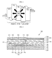
- Fig. 1 is a schematic view of an organic light emitting diode.
- Fig. 2 is a cross-sectional view of an organic light emitting diode in accordance with an embodiment of the present invention.
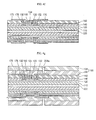
- Fig. 3 is a flowchart of a method of fabricating an organic light emitting display in accordance with an embodiment of the present invention.
- Figs. 4a to 4k are cross-sectional views of a fabrication method steps of an organic light emitting display in accordance with an embodiment of the present invention.
- FIG. 2 a cross-sectional view of an organic light emitting diode in accordance with an embodiment of the present invention.
- an organic light emitting display 100 includes a substrate 110, a buffer layer 120 arranged on the substrate 110, a semiconductor layer 130 arranged on the buffer layer 120, a gate insulating layer 140 arranged on the semiconductor layer 130, a gate electrode 150 arranged on the gate insulating layer 140, an inter-layer dielectric layer 160 arranged on the gate electrode 150, a source/drain electrode 170 arranged on the inter-layer dielectric layer 160, an insulating layer 180 arranged on the source/drain electrode 170, a non-transmissive layer 190 arranged on the insulating layer 180, an organic light emitting diode 200 arranged on the insulating layer 180, with a first part of the non-transmissive layer 190 forming part 202 of the organic light emitting diode, a pixel defining film 210 arranged on a second part of non-transmissive layer 190, the second part located outside the organic light emitting diode 200, and an anti-friction layer 220 arranged on
- the upper surface and the lower surface of the substrate 110 are parallel to each other, and a thickness between the upper and lower surfaces is formed to be 0.05 millimeters (mm) to 1 millimeters (mm). If the thickness is below 0.05mm, the substrate is easily damaged by cleaning, etching and heat treatment process, and is weak with respect to external forces. If the thickness is above 1mm, it is impossible to apply the substrate to various thin display devices.
- the substrate is formed of a material selected from a typical glass, plastic, polymer or an equivalent thereof. However, the present invention is not restricted to these materials.
- the buffer layer 120 is formed on the upper surface of the substrate 110.
- This buffer layer 120 prevents H 2 O, H 2 or H 2 , etc from infiltrating into the semiconductor layer 130 or the organic light emitting diode 200 through the substrate 110.
- the buffer layer 120 is made of at least one material selected from SiO 2 , Si 3 N 4 , inorganic film or an equivalent thereof.
- the present invention is not restricted to these materials.
- This buffer layer 120 may be omitted, if necessary.
- the semiconductor layer 130 is formed on the upper surface of the buffer layer 120.
- This semiconductor layer 130 is composed of source/drain regions 132 formed on both sides opposite to each other, and a channel region 134 formed between the source/drain regions 132.
- the semiconductor layer 130 may be a Thin Film Transistor (TFT).
- TFT Thin Film Transistor
- This TFT is at least one TFT selected from an amorphous Si TFT, poly Si TFT, organic TFT, micro Si TFT (with a grain size from the amorphous Si to the poly Si) or an equivalent thereof.
- the present invention is not restricted to these TFTs.
- the poly Si TFT may be formed by at least one method selected from a crystallization method using a laser at low temperature, a crystallization method using a metal, a crystallization method using high pressure, or the equivalent thereof.
- a crystallization method using a laser may be Excimer Laser Annealing (ELA), Sequential Lateral Solidification (SLS), Thin Beam Direction Crystallization (TDX) and so on.
- ELA Excimer Laser Annealing
- SLS Sequential Lateral Solidification
- TDX Thin Beam Direction Crystallization
- the present invention is not restricted to these methods.
- the crystallization method using a metal may be Solid Phases Crystallization (SPC), Metal Induced Crystallization (MIC), Metal Induced Lateral Crystallization (MILC), Super Grained Silicon (SGS) and so on.
- SPC Solid Phases Crystallization
- MIC Metal Induced Crystallization
- MILC Metal Induced Lateral Crystallization
- SGS Super Grained Silicon
- the present invention is not restricted to these methods.
- the thin film resistor may be one of PMOS, NMOS or an equivalent thereof.
- the present invention is not restricted thereto.
- the gate insulating layer 140 is formed on the upper surface of the semiconductor layer 130.
- the gate insulating layer 140 is also formed on the buffer layer 120 which extends beyond the semiconductor layer 130.
- the gate insulating layer 140 is formed of at least one of a silicon oxide film, a silicon nitride film, an inorganic film or an equivalent thereof.
- the present invention is not restricted to these materials.
- the gate electrode 150 is formed on the upper surface of the gate insulating layer 140. More specifically, the gate electrode 150 is formed on the gate insulating layer 140 corresponding to the channel region 134 of the semiconductor layer 130. As known to those skilled in the art, this gate electrode 150 makes channels of electrons or holes in the channel region 134 by applying an electric field to the channel region 134 of the gate insulating layer 140.
- the gate electrode 150 is formed of a typical metal (Mo, MoW, Ti, Cu, Al, A1Nd, Cr, Mo alloy, Cu alloy, Al alloy, etc.), a doped poly silicon or an equivalent thereof. However, the present invention is not restricted to these materials.
- the inter-layer dielectric layer 160 is formed on the upper surface of the gate electrode 150 and gate insulating layer 140.
- the inter-layer dielectric layer 160 is formed of at least one of a silicon oxide film, a silicon nitride film, a polymer, a plastic, a glass or an equivalent thereof.
- the present invention is not restricted to these materials.
- the source/drain electrode 170 is formed on the upper surface of the inter-layer dielectric layer 160.
- An electrically conductive contact 176 which perforates the inter-layer dielectric layer 160, is formed between the source/drain electrode 170 and the semiconductor layer 130. That is, the source/drain regions 132 of the semiconductor layer 130 and the source/drain electrode 170 are electrically coupled by the electrically conductive contact 176.
- the source/drain electrode 170 is formed of the same metal material as the gate electrode 150. However, the present invention is not restricted to this material.
- the above-described semiconductor layer 130 that is, the TFT
- the semiconductor layer 130 in accordance with an embodiment of the present invention is not restricted to the coplanar structure, and may have a different structure, for example, may be at least one of an inverted coplanar structure, a staggered structure, an inverted staggered structure or an equivalent thereof.
- the semiconductor layer 130 of the present invention is not restricted thereto.
- the insulating layer 180 is formed on the upper surface of the source/drain electrode 170 and the inter-layer dielectric layer 160.
- This insulating layer 180 is composed of a protective film 182 and an overcoat film 184.
- the protective film 182 covers the source/drain electrode 170 and the inter-layer dielectric layer 160, and protects the source/drain electrode 170 and so on.
- This protective film 182 is formed of one material selected from a typical inorganic film or an equivalent thereof. However, the material of the protective film 182 of the present invention is not restricted thereto.
- the overcoat film 184 covers the protective film 182.
- This overcoat film 184 makes the whole surface of the diode flat, and is formed of at least one material selected from a Benzo Cyclo Butene (BCB), an Acrylic or an equivalent thereof.
- BCB Benzo Cyclo Butene
- the present invention is not restricted to these materials.
- the non-transmissive layer 190 is formed on the entire upper surface of the insulating layer 180. That is, the non-transmissive layer 190 is formed on the upper surface of the insulating layer 180 directly above the semiconductor layer 130 and on the upper surface of the insulating layer 180 which is not directly above the semiconductor layer 130.
- the non-transmissive layer 190 is electrically coupled to the source/drain electrode 170 through the electrically conductive via 208 perforating the insulating layer 180. The reason why the non-transmissive layer 190 is electrically coupled to the source/drain electrode 170 is described later.
- the non-transmissive layer 190 prevents external UV-rays from infiltrating into the other substrate opposite to the UV-rays during the fabrication process which forms the organic light emitting diode 200 by bonding two substrates 110.
- the non-transmissive layer 190 prevents external UV-rays from infiltrating into the the organic light emitting diode 200 after the substrate 110 is divided into pieces.
- the non-transmissive layer 190 is formed of one material selected from a UV-ray protective agent or the equivalent. Furthermore, the non-transmissive layer 190 may be formed of at least one material selected from a metal through which UV-rays cannot be transmitted, a transparent UV-ray protective agent and an opaque UV-ray protective agent. Furthermore, if the non-transmissive layer 190 is the metal, then the non-transmissive layer is formed of at least one material selected from Cr, Cr 2 O 3 , Al, Au, Ag, MgO, silver alloy or an equivalent thereof. However, the present invention is not restricted to these materials.
- the non-transmissive layer 190 is formed to have a thickness of 50nm (500 Angstrom) to 300nm (3000 Angstrom). If the thickness of the non-transmissive layer 190 is below 50nm (500 Angstrom), then the elimination rate of UV-rays is low, and the semiconductor layer 130 or the organic light emitting diode 200 is affected by the radiation during or after the fabrication process. If the thickness of the non-transmissive layer 190 is above 300nm (3000 Angstrom), then the elimination rate of UV-rays is good but the non-transmissive layer 190 is too thick.
- the organic light emitting diode 200 is formed only using a certain region of the non-transmissive layer 190.
- This organic light emitting diode 200 includes an anode 202, an organic light emitting thin film 204 formed on the upper surface of the anode 202, and a cathode 206 formed on the upper surface of the organic light emitting thin film 204.
- the anode 202 is formed of at least one of ITO (Indium Tin Oxide)/Ag, ITO/Ag/ITO, ITO/Ag/IZO(Indium Zinc Oxide) or an equivalent thereof.
- ITO Indium Tin Oxide
- ITO/Ag/ITO ITO/Ag/IZO(Indium Zinc Oxide) or an equivalent thereof.
- the present invention is not restricted to these materials.
- the ITO is a transparent electrically conductive film which a hole injection barrier to the organic light emitting thin film 204 is small due to a constant work function
- said Ag is a film which reflects the light of the organic light emitting thin film 204 into the upper surface.
- the organic light emitting thin film 204 is composed of an EMitting Layer (EML) which is emitted as the exciton is formed by joining the electrons and holes, an Electron Transport Layer (ETL) which controls the speed of electrons appropriately, and a Hole Transport Layer (HTL) which controls the speed of holes appropriately.
- EIL Electron Injection Layer
- HIL Hole Injection Layer
- the cathode 206 is at least one of Al, MgAg alloy, MgCa alloy or an equivalent thereof.
- the present invention is not restricted to these materials.
- the Al should be thin, and the resistance is increased, and thus the electron injection barrier is increased.
- the MgAg alloy has a lower electron injection barrier than that of the Al
- the MgCa alloy has a lower electron injection barrier than that of the MgAg. Therefore, in case of the front-emitting display; it is preferable that the MgAg alloy and the MgCa alloy are used as the cathode 206.
- the MgAg alloy and the MgCa alloy are sensitive to external environment and form an insulating layer by oxidation, and thus, perfect sealing is needed.
- the anode 202 of the organic light emitting diode 200, and the non-transmissive layer 190 are of substantially the same material. That is, the non-transmissive layer 190 is formed on the entire upper surface of the insulating layer, and the region of the non-transmissive layer 190 in which the organic light emitting diode 200 is formed, is referred to as the anode 202. Therefore, the non-transmissive layer 190 is formed of at least one material selected from ITO, ITO/Ag, ITO/Ag/ITO, ITO/Ag/IZO or an equivalent thereof as is the anode 202.
- the non-transmissive layer 190 is electrically coupled to the source/drain electrode 170 by the electrically conductive via 208, since part of the non-transmissive layer 190 is used as the anode 202 of the organic light emitting diode 200.
- the present invention may be applied to both a bottom-emitting display which emits toward the bottom of the substrate 110, and a surface-emitting display which emits toward both surfaces of the substrate 110, although the present invention has been mainly explained with reference to the front-emitting display.
- the pixel defining film 210 as an outer periphery of the organic light emitting diode 200, is formed on the upper surface of the non-transmissive layer 190.
- This pixel defining film 210 forms a clear boundary between a red organic light emitting diode, a green organic light emitting diode and a blue organic light emitting diode, and thus clearly defines the emitting boundary region between the pixels.
- the pixel defining film 210 is formed of at least one of polyimide or an equivalent thereof. However, the material of the pixel defining film 210 is not limited thereto.
- the anti-friction layer 220 is formed on the lower surface of the substrate 110.
- This anti-friction layer 220 prevents two substrates 110 from contacting each other during the fabrication process which forms the semiconductor 130 and the organic light emitting diode 200 by bonding two substrates 110. Furthermore, this anti-friction layer 220 prevents the substrate from bending or breaking during the transport process, since a specific rigidity is obtained by thickening the overall thickness when the two substrates are bonded.
- This anti-friction layer 220 is formed of one material selected from an organic material, an inorganic material or an equivalent thereof. However, the material is not limited thereto.
- the anti-friction layer 220 is formed to have a thickness of 10 micro-meters ( ⁇ m) to 100 micro-meters ( ⁇ m).
- ⁇ m micro-meters
- ⁇ m micro-meters
- ⁇ m micro-meters
- Fig. 3 is a flowchart of a method of fabricating an organic light emitting display in accordance with an embodiment of the present invention.
- a method of fabricating an organic light emitting display in accordance with an embodiment of the present invention includes preparing substrates (S1), bonding the substrates (S2), forming a buffer layer (S3), forming a semiconductor layer (S4), forming an insulating layer (S5), forming an non-transmissive layer (S6), forming an organic light emitting diode (S7), separating the substrates (S8), and removing an anti-friction layer (S9).
- Figs. 4a to 4k. are cross-sectional views of a method of fabricating an organic light emitting display in accordance with an embodiment of the present invention.
- substrates 110 having flat upper and lower surfaces and having a constant thickness are provided.
- the substrates 110 are formed of one material selected from glass, plastic, steel or polymers. However, the material of the substrates 110 in accordance with an embodiment of the present invention is not limited thereto. It is preferable that the thickness of the substrates 110 is 0.05mm to 1mm. When the thickness is below 0.05mm, the substrates are easily damaged by cleaning, etching and heat treatment process, and are weak with respect to external forces. When the thickness is above 1 mm, it is impossible to apply the substrates to various thin display devices.
- two substrates 110 are prepared and bonded to each other.
- an anti-friction layer 220 is provided between the two substrates 110.
- This anti-friction layer 220 is formed by depositing or coating at least one of an organic material, an inorganic material or an equivalent thereof.
- the material or the forming method of the anti-friction layer 220 is not restricted thereto. It is preferable that this anti-friction layer 220 is made of a material which is easily taken off, if the friction layer 220 is removed after completing the organic light emitting display. This material may be a photo resist of an organic material, for example. However, the material is not limited thereto.
- a bonding agent (not illustrated in drawings) is applied to a certain area or entire area of the substrates 110 to prevent the two substrates 110 from separating during the fabricating process.
- This bonding agent is at least one of a typical epoxy bonding agent, an UV-ray cured bonding agent or an equivalent thereof.
- the material is not limited thereto.
- the anti-friction layer 220 may be formed on the substrates 110 in advance, and the two anti-friction layers 220 then bonded to each other. However, the anti-friction layer 220 may be formed by injecting a liquid anti-friction layer 220 into the gap between the two substrates 110.
- a liquid anti-friction layer 220 is injected into the gap between the two substrates 110, and flows into the gap with ease by a capillary action. It is preferable that the anti-friction layer 220 is cured by heat treating at a certain temperature after the liquid anti-friction layer 220 is formed.
- the buffer layer 120 having a constant thickness is formed on the surface of the substrates 110 which is opposite to the surface in which the anti-friction layer 220 is formed.
- This buffer layer 120 is formed of at least one of a silicon oxide film, a silicon nitride film or an equivalent thereof.
- the material of the buffer layer 120 is not limited thereto.
- the buffer layer 120 prevents H 2 O, H 2 , H 2 , or and so on from infiltrating into the semiconductor layer 130 or the organic light emitting diode 190 through the substrate 110.
- the buffer layer 120 assists the semiconductor layer 130 and so on to be formed on the surface of the buffer layer 120.
- the buffer layer 120 may be formed on one substrate 110 and then formed on the other substrate 110 in sequence, or the buffer layer may be formed on both substrates 110 simultaneously.
- step (S4) of forming the semiconductor layer 130 the semiconductor layer 130 is formed on the surface of the buffer layer 120, and the gate insulating layer 140 is formed thereon.
- Forming the semiconductor layer 130 includes forming source/drain regions 132 on opposite sides thereof, and then forming a channel region 134 between the source/drain regions 132.
- the semiconductor layer 130 is a TFT selected from at least one an amorphous Si TFT, poly Si TFT, organic TFT, micro Si TFT (with a grain size from the amorphous Si to the poly Si) or an equivalent thereof.
- the present invention is not limited to these TFTs.
- the TFT is a poly Si TFT
- the poly Si TFT is formed from at least one method selected from a crystallization method using a laser at low temperature, a crystallization method using a metal, a crystallization method using high pressure, or an equivalent thereof.
- the present invention is not limited to these methods.
- the amorphous silicon is formed by at least one method selected from Plasma Enhanced Chemical Vapor Deposition (PECVD), Low Pressure Chemical Vapor Deposition (LPCVD), sputtering, or an equivalent thereof.
- PECVD Plasma Enhanced Chemical Vapor Deposition
- LPCVD Low Pressure Chemical Vapor Deposition
- sputtering or an equivalent thereof.
- the method of forming the amorphous silicon is not limited thereto.
- a desired number of semiconductor layers 130 are formed in the desired position by means of photo resist, coating, exposure, development, etching, photo resist peeling and so on.
- a method of crystallizing the amorphous silicon into poly silicon includes Excimer Laser Annealing (ELA), Sequential Lateral Solidification (SLS), Thin Beam Direction Crystallization (TDX) or an equivalent thereof.
- ELA Excimer Laser Annealing
- SLS Sequential Lateral Solidification
- TDX Thin Beam Direction Crystallization
- a crystallization method using a metal includes Solid Phases Crystallization (SPC), Metal Induced Crystallization (MIC), Metal Induced Lateral Crystallization (MILC), Super Grained Silicon (SGS) or an equivalent thereof.
- SPC Solid Phases Crystallization
- MIC Metal Induced Crystallization
- MILC Metal Induced Lateral Crystallization
- SGS Super Grained Silicon
- the thin film resistor may be one of PMOS, NMOS or an equivalent thereof.
- the electrically conductive type thereof is not limited thereto.
- the gate insulating layer 140 having a constant thickness may be formed on the surface of the semiconductor layer 130 by at least one method selected from PECVD, LPCVD, sputtering or an equivalent thereof. However, the method is not limited thereto.
- the gate insulating layer 140 may also be formed on the buffer layer 120 which is an outer periphery of the semiconductor layer 130.
- the gate insulating layer 140 is formed of at least one of a silicon oxide film, a silicon nitride film, an inorganic film or an equivalent thereof. However, the material is not limited thereto.
- the gate electrode 150 is formed on the upper surface of the gate insulating layer 140 by a method selected from PECVD, LPCVD, sputtering or an equivalent thereof.
- a desired number of gate electrodes 150 is formed in the desired position by a photo resist, coating, exposure, development, etching, photo resist peeling and so on.
- the gate electrode 150 is formed on the gate insulating layer 140 corresponding to the channel region 134 of the semiconductor layer 130.
- the gate electrode 150 forms a channel of holes or electrons in the channel region 134 by applying an electric field on the channel region 134 of the lower part of the gate insulating layer 140.
- the gate electrode 150 is formed of a typical metal (Mo, MoW, Ti, Cu, Al, A1Nd, Cr, Mo alloy, Cu alloy, Al alloy, and etc.), a doped poly silicon or an equivalent thereof.
- a typical metal Mo, MoW, Ti, Cu, Al, A1Nd, Cr, Mo alloy, Cu alloy, Al alloy, and etc.
- the material is not limited thereto.
- the inter-layer dielectric layer 160 is formed on the upper surface of the gate electrode 150 and gate insulating layer 140.
- the inter-layer dielectric layer 160 is formed of at least one of a silicon oxide film, a silicon nitride film, a polymer, a plastic, a glass or an equivalent thereof, However, the material of the inter-layer dielectric layer 160 is not limited thereto.
- the region of the inter-layer dielectric layer 160 which corresponds to the source/drain region 132 is exposed to the outside by the etching process. The exposed region is referred to as a contact hole, and a contact is subsequently formed on the contact hole.
- the source/drain electrode 170 is formed on the inter-layer dielectric layer by one method selected from PECVD, LPCVD, sputtering or an equivalent thereof. After the above described deposition process, a desired number of source/drain electrodes 170 is formed in the desired positions by a photo resist, coating, exposure, development, etching, photo resist peeling and so on.
- An electrically conductive contact 176 is formed between the source/drain electrode 170 and the source/drain regions 132 of the semiconductor layer 130. The electrically conductive contact 176 is formed by filling the preformed contact hole.
- the semiconductor layer 130 and the source/drain electrode 170 are electrically coupled by the electrically conductive contact 176.
- the electrically conductive contact 176 is formed of the same material as the gate electrode 150 and the source/drain electrode 170. However, the material of the electrically conductive contact 176 is not limited thereto.
- the source/drain electrode 170 is formed of the same metal material as the gate electrode 150. However, the material is not limited thereto.
- the above-described semiconductor layer 130 (that is, the TFT) is defined as a coplanar structure.
- the semiconductor layer 130 is not limited to the coplanar structure, and may be other structures known hereto, for example, at least one of an inverted coplanar structure, a staggered structure, an inverted staggered structure or an equivalent thereof. However, the semiconductor layer 130 is not limited thereto.
- the semiconductor layer 130, the gate insulating layer 140, the gate electrode 150, the inter-layer dielectric layer 160 and the source/drain electrode 170 are formed on the substrate 110 of one side and then formed on the substrate 110 of the other side. That is, the semiconductor layer 130, the gate insulating layer 140, the gate electrode 150, the inter-layer dielectric layer 160 and the source/drain electrode 170 are completed on the one substrate 110, and the semiconductor layer 130, the gate insulating layer 140, the gate electrode 150, the inter-layer dielectric layer 160 and the source/drain electrode 170 are completed on the other substrate 110. Furthermore, the constituent diodes 130, 140, 150, 160, and 170 are formed in sequence by flipping one and the other substrates. Furthermore, the constituent diodes 130, 140, 150, 160, and 170 may be completed by forming them on both substrates, if the processing devices are sufficient.
- step (S5) the insulating layer 180 having a constant thickness is formed on the semiconductor layer 130 (i.e. the upper surface of the source/drain electrode 170 and the inter-layer dielectric layer 160).
- This insulating layer 180 is composed of a protective film 182 and an overcoat film 184.
- the protective film 182 covers the source/drain electrode 170 and the inter-layer dielectric layer 160, and protects the source/drain electrode 170, the gate electrode 150 and so on.
- the via hole 208a is formed in advance by etching the protective film 182 and the overcoat film 184 in the area which corresponds to the source/drain electrode 170.
- the protective film 182 is formed of one material selected from a typical inorganic film or an equivalent thereof. However, the material of the protective film 182 is not limited thereto.
- the overcoat film 184 covers the protective film 182. This overcoat film 184 makes the entire surface of the diode flat, and is formed of at least one material selected from a Benzo Cyclo Butene (BCB), an Acrylic or an equivalent thereof. However. the material is not limited thereto.
- BCB Benzo Cyclo Butene
- the insulating layer 180 is formed on one side of the substrate 110, and then formed on the other side of the substrate 110. That is, the insulating layer 180 is completed on the one substrate 110, and the insulating layer 180 is completed on the other substrate 110. Furthermore, the insulating layer 180 may be formed in sequence by flipping one and the other substrates. Furthermore, the insulating layer 180 may be formed them on both substrates, if the processing devices are sufficient.
- the non-transmissive layer 190 having a constant thickness is formed on the entire upper surface of the insulating layer 180. That is, the non-transmissive layer 190 is formed on the upper surface directly over the semiconductor layer 130 and on the upper surface not directly over the semiconductor layer 130.
- the non-transmissive layer 190 is electrically coupled to the source/drain electrode 170 through the electrically conductive via 208.
- the non-transmissive layer 190 prevents UV-rays from infiltrating into other substrate opposite to the UV-rays during the fabricating process that forms the organic light emitting diode 200 by bonding two substrates 110.
- the non-transmissive layer 190 prevents external UV-rays from infiltrating into the the organic light emitting diode 200 after the substrate 110 is divided into pieces.
- the non-transmissive layer 190 is formed of a UV-ray protective agent or an equivalent. Furthermore, the non-transmissive layer 190 may be formed of at least one of a metal through which UV-ray cannot be transmitted, a transparent UV-ray protective agent or an opaque UV-ray protective agent. Furthermore, if the non-transmissive layer 190 is a metal, then the non-transmissive layer 190 is formed of at least one material selected from Cr, Cr 2 O 3 , Al, Au, Ag, MgO, a silver alloy or an equivalent thereof. However, the material is not limited thereto.
- the non-transmissive layer 190 is formed to have a thickness of 50nm (500 ⁇ ) to 300nm (3000 ⁇ ). If the thickness of the non-transmissive layer 190 is below 50nm (500 ⁇ ), then the elimination rate of UV-rays is low, and thus the semiconductor layer 130 or the organic light emitting diode 200 is affected by UV-rays during or after the fabrication process. If the thickness of the non-transmissive layer 190 is above 300nm (3000 ⁇ ), then the elimination rate of UV-rays is good. However, the the non-transmissive layer 190 is too thick.
- the non-transmissive layer 190 is formed by at least one method selected from Plasma Enhanced Chemical Vapor Deposition (PECVD), Low Pressure Chemical Vapor Deposition (LPCVD), sputtering or an equivalent thereof.
- PECVD Plasma Enhanced Chemical Vapor Deposition
- LPCVD Low Pressure Chemical Vapor Deposition
- sputtering or an equivalent thereof.
- the method of forming the non-transmissive layer 190 is not restricted thereto.
- the non-transmissive layer 190 may be formed on one substrate 110, and then formed on the other substrate 110 in sequence, or may be formed on both substrates 110 simultaneously.
- step (S7) the organic light emitting diode 200 is formed on a certain area of the non-transmissive layer 190 as a thin film.
- the non-transmissive layer 190 used as the anode 202, the organic light emitting thin film 204 and the cathode 206 are formed in sequence.
- the anode 202 is formed of at least one material selected from ITO, ITO/Ag, ITO/Ag/ITO, ITO/Ag/IZO or an equivalent thereof.
- the material or the method of forming the anode 202 is not limited thereto.
- the anode 202 is formed by one method of RF sputtering, DC sputtering, ion-beam sputtering or vacuum evaporation. After that, a desired area of the anode is formed in the desired position by a photo resist, coating, exposure, development, etching, photo resist peeling and so on.
- the anode 202 is electrically coupled to the source/drain electrode 170 through the electrically conductive via 208 perforating the insulating layer 180.
- a region of the non-transmissive layer 190 is used as the anode of the organic light emitting diode 200. Therefore, the material of the non-transmissive layer 190 is substantially the same as that of the anode 202. That is, the non-transmissive layer 190 is formed of at least one of ITO/Ag, ITO/Ag/ITO, ITO/Ag/IZO or an equivalent thereof. Furthermore, the anode 202 is electrically coupled to the source/drain electrode 170 through the electrically conductive via 208 as described above, since the region of the non-transmissive layer 190 is used as the anode of the organic light emitting diode 200.
- the ITO serves as a small transparent electrically conductive film having a low hole injection barrier against the organic light emitting thin film 204 due to a constant work function, said Ag reflects the light from the organic light emitting thin film 204 in the front-emitting display.
- the organic light emitting thin film 204 is composed of at least one of a Hole Injecting Layer (HIL) that improves the injection efficiency of the hole, a Hole Transport Layer (HTL) that controls the moving speed of the hole appropriately, an EMitting Layer (EML) that emits light by forming an exciton, an Electron Transport Layer (ETL) that controls the moving speed of the electrons, or an Electron Injection Layer (EIL) that improves the injection efficiency of the electrons in sequence.
- HIL Hole Injecting Layer
- HTL Hole Transport Layer
- EML Electron Transport Layer
- EIL Electron Injection Layer
- the organic light emitting thin film 204 may be formed by a wet coating method such as a spin coating that applies the thin film as a liquid, a deep coating, a spray method, a screen printing method, an ink-jet printing method and so on, or by a dry coating method such as sputtering, vacuum evaporation and so on.
- a wet coating method such as a spin coating that applies the thin film as a liquid, a deep coating, a spray method, a screen printing method, an ink-jet printing method and so on
- a dry coating method such as sputtering, vacuum evaporation and so on.
- the cathode 206 is formed on the Electron Injection Layer (EIL) of the organic light emitting thin film.
- the cathode 206 is formed by depositing at least one of Al, MgAg alloy, MgCa alloy or an equivalent.
- the material or the forming method is not limited thereto.
- the cathode 206 may be formed by one of RF sputtering, DC sputtering, ion-beam sputtering or a vacuum evaporation method. After that, a desired area of the cathode 206 is formed in the desired position by a photo resist, coating, exposure, development, etching, photo resist peeling and so on.
- the front-emitting display is chosen and if Al is used as the cathode 206, then it must be very thin to increase its light emitting rate, and thus, the electron injection barrier may be increased as the resistance is increased. Therefore, at least one of an MgAg alloy, an MgCa alloy or an equivalent thereof may be used as the cathode 206.
- the cathode 206 may also be formed of one of ITO or IZO.
- the MgAg alloy and the MgCa alloy are sensitive to external environment and form the insulating layer by oxidation, and thus, a perfect seal is required.
- the pixel defining film 210 is formed on the non-transmissive layer 190 to clearly define the boundary between the organic light emitting diodes 200 after the cathode 206 is completed.
- This pixel defining film 210 is formed of at least one of a polyimide or an equivalent thereof.
- the organic light emitting diode 200 is exposed to the outside by a photo resist, coating, exposure, development, etching, photo resist peeling and so on after this coating or deposition is completed.
- the present invention may be applied to both a bottom-emitting display which emits light toward the bottom of the substrate 110, and to a surface-emitting display which emits light toward both surfaces of the substrate 110.
- the present invention has been explained with reference to the front-emitting display.
- the organic light emitting diode 200 is formed on one side of the substrate 110 and then formed on the other side of the substrate 110. That is, the organic light emitting diode 200 is first completed on one substrate 110, and the organic light emitting diode 200 is then completed on the other substrate 110. Furthermore, the organic light emitting diode 200 may be formed in sequence by flipping one and the other substrates100. Furthermore, the organic light emitting diode 200 may be completed by being formed on both substrates 110, if the processing devices are sufficient.
- step (S8) the respective substrates 110 are bonded and processed and then separated. That is, the bonding agent which bonds the two substrates 110 together is removed by a sawing tool, etc, to separate the respective substrates 110. If the anti-friction layer 220 is formed on the substrates 110, then the respective substrates 110 are separated with ease. However, if the bonding agent is applied to the respective substrates 110 and the anti-friction layer 220 in a liquid phase is injected into the gap between the substrates 110, then the respective substrates 110 are separated by a chemical solution which dissolves the anti-friction layer 220.
- the anti-friction layer 220 may remain on one side of the substrate 110 after the substrates 110 are separated. Furthermore, while not illustrated in the drawings, a bonding process, which bonds an encapsulation substrate using an encapsulation material, may be further included. A transparent absorbent may be formed on the encapsulation substrate to absorb the moisture.
- the present invention is completed with the separation of the substrates 110. That is, after the separation step, the display is marketed as the product, after a cell test, Flexible Printed Circuit (FPC) bonding, module test and reliability test have been completed.
- the cell test may be achieved by forming a region for the cell test on the substrate 110 before the sawing step.
- the anti-friction layer 230 may remain on one side of the substrate 110 of the light emitting display device 100. This anti-friction layer 230 may prevent the UV-rays from infiltrating as well as protecting the surface of the substrate 110 from the external environment.
- the thickness of the substrate 110 is 0.5mm, and is regarded as a bonded substrate having a thickness of 1mm or more, since the fabrication process is accomplished by bonding two substrates together. Therefore, the bending or breaking phenomenon is prevented as the rigidity is increased, and the semiconductor layer forming process and the organic light emitting diode forming process are easily achieved.
- the substrates are separated into respective substrates, and thus it is possible to get a thin substrate having a thickness of 0.5mm.
- the anti-friction layer removing step (S9) as shown in Fig. 4k the anti-friction layer 220 formed on the substrate 110 is removed. That is, the anti-friction layer 220 is removed from the substrate 110 by using a specific chemical solution or by using a grinding machine. Therefore, if the anti-friction layer 220 is removed, no anti-friction layer 220 remains on the surface of the substrate 110 of the organic light emitting display, and the device is thin. Of course, the anti-friction layer 220 may remain for blocking UV-rays or for protecting against external impact. However, the non-transmissive layer 190 is already formed in the substrate 110, and thus the remaining of the anti-friction layer 220 is required.
- the organic light emitting display in accordance with an embodiment of the present invention is applied to electronic appliances, such as cellular telephones, Personal Digital Assistants (PDAs), notebook computers, computer monitors and television sets, so that they may be easily fabricated to be thin and compact by including a substrate with a thickness of 0.05mm to 1mm.
- electronic appliances such as cellular telephones, Personal Digital Assistants (PDAs), notebook computers, computer monitors and television sets, so that they may be easily fabricated to be thin and compact by including a substrate with a thickness of 0.05mm to 1mm.
- the organic light emitting display in accordance with an embodiment of the present invention prevents UV-rays from influencing the organic light emitting diodes through the substrate during use by forming the non-transmissive layer in the lower part of the organic light emitting diodes.
- the method of fabricating the organic light emitting display in accordance with an embodiment of the present invention shortens the overall processing time by 50% as the semiconductor processing and the organic thin film processing (including cleaning, etching, exposure, development and heat treatment) are executed simultaneously by bonding two substrates having a thickness of 0.05mm to 1mm together.
- the method of fabrication in accordance with an embodiment of the present invention prevents UV-rays from infiltrating to the other substrate during exposure processing by forming the non-transmissive layer in the lower part of the organic light emitting diode.
- the method of fabrication in accordance with an embodiment of the present invention prevents the substrate from bending or breaking during fabrication processes as rigidity is increased by forming the anti-friction layer having a specific thickness between the substrates to be bonded.
- the method of fabrication in accordance with an embodiment of the present invention prevents the substrates from contacting each other, and thus, from being damaged by forming the anti-friction layer between the substrates.
Landscapes
- Engineering & Computer Science (AREA)
- Manufacturing & Machinery (AREA)
- Microelectronics & Electronic Packaging (AREA)
- Physics & Mathematics (AREA)
- Optics & Photonics (AREA)
- Electroluminescent Light Sources (AREA)
- Devices For Indicating Variable Information By Combining Individual Elements (AREA)
Applications Claiming Priority (1)
| Application Number | Priority Date | Filing Date | Title |
|---|---|---|---|
| KR1020060111298A KR100824881B1 (ko) | 2006-11-10 | 2006-11-10 | 유기 전계 발광 표시 장치 및 그 제조 방법 |
Publications (2)
| Publication Number | Publication Date |
|---|---|
| EP1921690A2 true EP1921690A2 (de) | 2008-05-14 |
| EP1921690A3 EP1921690A3 (de) | 2011-03-09 |
Family
ID=38828655
Family Applications (1)
| Application Number | Title | Priority Date | Filing Date |
|---|---|---|---|
| EP07252179A Withdrawn EP1921690A3 (de) | 2006-11-10 | 2007-05-25 | Organische lichtemittierende Anzeige und Verfahren zu ihrer Herstellung |
Country Status (5)
| Country | Link |
|---|---|
| US (1) | US8536567B2 (de) |
| EP (1) | EP1921690A3 (de) |
| JP (2) | JP2008124420A (de) |
| KR (1) | KR100824881B1 (de) |
| CN (1) | CN100583492C (de) |
Families Citing this family (16)
| Publication number | Priority date | Publication date | Assignee | Title |
|---|---|---|---|---|
| KR100824881B1 (ko) | 2006-11-10 | 2008-04-23 | 삼성에스디아이 주식회사 | 유기 전계 발광 표시 장치 및 그 제조 방법 |
| KR100770127B1 (ko) * | 2006-11-10 | 2007-10-24 | 삼성에스디아이 주식회사 | 유기 전계 발광 표시 장치 및 그 제조 방법 |
| KR100824880B1 (ko) * | 2006-11-10 | 2008-04-23 | 삼성에스디아이 주식회사 | 유기 전계 발광 표시 장치 및 그 제조 방법 |
| KR100833738B1 (ko) | 2006-11-30 | 2008-05-29 | 삼성에스디아이 주식회사 | 유기 전계 발광 표시 장치 및 그 제조 방법 |
| KR100824902B1 (ko) * | 2006-12-13 | 2008-04-23 | 삼성에스디아이 주식회사 | 유기 전계 발광 표시 장치 및 그 제조 방법 |
| KR101383454B1 (ko) * | 2007-09-21 | 2014-04-08 | 엘지디스플레이 주식회사 | 전계발광소자 |
| WO2010016206A1 (ja) * | 2008-08-04 | 2010-02-11 | パナソニック株式会社 | フレキシブル半導体装置の製造方法 |
| KR101084263B1 (ko) * | 2009-12-14 | 2011-11-16 | 삼성모바일디스플레이주식회사 | 유기 발광 표시 장치 |
| KR102034870B1 (ko) | 2012-12-18 | 2019-10-22 | 삼성디스플레이 주식회사 | 유기 발광 표시 장치 및 이의 제조 방법 |
| CN104425542B (zh) * | 2013-08-26 | 2017-08-04 | 昆山工研院新型平板显示技术中心有限公司 | 一种有机发光显示装置及其制备方法 |
| KR102315824B1 (ko) * | 2014-06-27 | 2021-10-20 | 엘지디스플레이 주식회사 | 유기 발광 표시 장치 및 그의 제조 방법 |
| CN104300085A (zh) | 2014-10-31 | 2015-01-21 | 京东方科技集团股份有限公司 | 有机电致发光器件以及显示装置 |
| CN105810844B (zh) * | 2016-03-23 | 2018-05-29 | 武汉华星光电技术有限公司 | Oled器件及其制作方法、柔性显示单元 |
| KR102573853B1 (ko) | 2016-09-20 | 2023-09-01 | 삼성디스플레이 주식회사 | 발광 표시 장치 |
| CN106784412B (zh) * | 2017-03-30 | 2019-02-26 | 武汉华星光电技术有限公司 | 柔性有机发光二极管显示器及其制作方法 |
| CN110752236B (zh) * | 2019-10-29 | 2022-05-24 | 京东方科技集团股份有限公司 | 一种显示基板及其制备方法、显示装置 |
Citations (1)
| Publication number | Priority date | Publication date | Assignee | Title |
|---|---|---|---|---|
| EP1906467A2 (de) * | 2006-09-28 | 2008-04-02 | Samsung SDI Co., Ltd. | Organische lichtemittierende Anzeige und Verfahren zu ihrer Herstellung sowie Vorrichtung zu ihrer Bewegung |
Family Cites Families (86)
| Publication number | Priority date | Publication date | Assignee | Title |
|---|---|---|---|---|
| JPS5917810B2 (ja) | 1975-06-12 | 1984-04-24 | セイコーエプソン株式会社 | 回路基板の製造方法 |
| AU572615B2 (en) * | 1983-12-27 | 1988-05-12 | Sony Corporation | Electrically conductive adhesive sheet circuit board and electrical connection structure |
| US5504605A (en) * | 1993-06-02 | 1996-04-02 | Hitachi, Ltd. | Liquid crystal display module having cut-away portions of the back frame for weight reduction and heat dissipation |
| JP3364081B2 (ja) | 1995-02-16 | 2003-01-08 | 株式会社半導体エネルギー研究所 | 半導体装置の作製方法 |
| JPH0980476A (ja) * | 1995-09-12 | 1997-03-28 | Nec Corp | アクティブマトリックス基板とその製造方法 |
| JPH09211482A (ja) | 1996-01-31 | 1997-08-15 | Sharp Corp | 液晶表示装置 |
| US5986401A (en) * | 1997-03-20 | 1999-11-16 | The Trustee Of Princeton University | High contrast transparent organic light emitting device display |
| JP3874871B2 (ja) | 1997-02-10 | 2007-01-31 | シャープ株式会社 | 液晶表示装置の製造方法 |
| JP2000150145A (ja) | 1998-11-02 | 2000-05-30 | Toyota Motor Corp | El素子の密封方法 |
| EP1127381B1 (de) * | 1998-11-02 | 2015-09-23 | 3M Innovative Properties Company | Transparente leitfähige oxide für kunststoff-flachbildschirme |
| JP3450213B2 (ja) | 1999-03-18 | 2003-09-22 | Necエレクトロニクス株式会社 | フラットパネル型表示装置 |
| JP2000298264A (ja) | 1999-04-13 | 2000-10-24 | Samukon:Kk | 液晶表示装置用ガラス基板の製造方法とそれを用いた液晶表示装置 |
| US6573652B1 (en) * | 1999-10-25 | 2003-06-03 | Battelle Memorial Institute | Encapsulated display devices |
| US6384427B1 (en) * | 1999-10-29 | 2002-05-07 | Semiconductor Energy Laboratory Co., Ltd. | Electronic device |
| US6559594B2 (en) * | 2000-02-03 | 2003-05-06 | Semiconductor Energy Laboratory Co., Ltd. | Light-emitting device |
| JP2001267578A (ja) * | 2000-03-17 | 2001-09-28 | Sony Corp | 薄膜半導体装置及びその製造方法 |
| JP2001319776A (ja) | 2000-05-12 | 2001-11-16 | Semiconductor Energy Lab Co Ltd | Elパネルの作製方法 |
| US6770518B2 (en) * | 2001-01-29 | 2004-08-03 | Semiconductor Energy Laboratory Co., Ltd. | Method for manufacturing a semiconductor device |
| US7083863B2 (en) * | 2001-02-21 | 2006-08-01 | Matsushita Electric Industrial Co., Ltd. | Luminous element and method for preparation thereof |
| JP2002350833A (ja) | 2001-05-30 | 2002-12-04 | Matsushita Electric Ind Co Ltd | 液晶表示装置およびその製造方法 |
| US6735982B2 (en) * | 2001-07-12 | 2004-05-18 | Intel Corporation | Processing relatively thin glass sheets |
| KR100782937B1 (ko) * | 2001-07-24 | 2007-12-07 | 엘지.필립스 엘시디 주식회사 | 유기전계발광소자 |
| US6660547B2 (en) * | 2001-07-26 | 2003-12-09 | Osram Opto Semiconductors Gmbh | Stabilization for thin substrates |
| FR2829723B1 (fr) * | 2001-09-14 | 2004-02-20 | Saint Gobain | Vitrage de securite fonctionnalise |
| KR100944886B1 (ko) * | 2001-10-30 | 2010-03-03 | 가부시키가이샤 한도오따이 에네루기 켄큐쇼 | 반도체 장치의 제조 방법 |
| US6731064B2 (en) * | 2001-11-20 | 2004-05-04 | International Business Machines Corporation | Yield enchancement pixel structure for active matrix organic light-emitting diode displays |
| KR100656490B1 (ko) * | 2001-11-26 | 2006-12-12 | 삼성에스디아이 주식회사 | 풀칼라 유기전계 발광표시소자 및 그의 제조방법 |
| KR100483988B1 (ko) * | 2001-11-29 | 2005-04-15 | 삼성에스디아이 주식회사 | 투명도전막의 투과도 변형방법 |
| JP2003173872A (ja) | 2001-12-06 | 2003-06-20 | Sony Corp | アライメント方法、パターン形成方法及びアライメント装置、並びに有機エレクトロルミネッセンス表示装置及びその製造方法 |
| KR100491143B1 (ko) | 2001-12-26 | 2005-05-24 | 삼성에스디아이 주식회사 | 블랙매트릭스를 구비한 평판표시장치 및 그 제조방법 |
| KR100491144B1 (ko) * | 2001-12-26 | 2005-05-24 | 삼성에스디아이 주식회사 | 평판표시장치 및 그의 제조방법 |
| US6953735B2 (en) * | 2001-12-28 | 2005-10-11 | Semiconductor Energy Laboratory Co., Ltd. | Method for fabricating a semiconductor device by transferring a layer to a support with curvature |
| US6815723B2 (en) * | 2001-12-28 | 2004-11-09 | Semiconductor Energy Laboratory Co., Ltd. | Light emitting device, method of manufacturing the same, and manufacturing apparatus therefor |
| KR100845557B1 (ko) * | 2002-02-20 | 2008-07-10 | 삼성전자주식회사 | 액티브 매트릭스형 유기전계발광 표시장치 및 그 제조방법 |
| JP2003282235A (ja) | 2002-03-25 | 2003-10-03 | Sanyo Electric Co Ltd | 有機エレクトロルミネッセンス表示装置 |
| TW595254B (en) | 2002-03-29 | 2004-06-21 | Sanyo Electric Co | Electroluminescense display device |
| JP2003317953A (ja) | 2002-04-26 | 2003-11-07 | Seiko Epson Corp | 有機エレクトロルミネッセンス装置の製造方法、有機エレクトロルミネッセンス装置、有機エレクトロルミネッセンス装置の製造装置及び電子機器 |
| TWI272641B (en) | 2002-07-16 | 2007-02-01 | Semiconductor Energy Lab | Method of manufacturing a semiconductor device |
| JP4693411B2 (ja) | 2002-10-30 | 2011-06-01 | 株式会社半導体エネルギー研究所 | 半導体装置の作製方法 |
| JP2004170910A (ja) | 2002-10-31 | 2004-06-17 | Seiko Epson Corp | 電気光学装置及び電子機器 |
| JP2004192969A (ja) * | 2002-12-12 | 2004-07-08 | Hitachi Displays Ltd | 有機el表示装置 |
| JP4218338B2 (ja) | 2002-12-24 | 2009-02-04 | セイコーエプソン株式会社 | 液晶表示装置の製造方法 |
| KR100904523B1 (ko) * | 2002-12-26 | 2009-06-25 | 엘지디스플레이 주식회사 | 액티브 매트릭스형 유기전계발광 소자용 박막트랜지스터 |
| JP4373085B2 (ja) * | 2002-12-27 | 2009-11-25 | 株式会社半導体エネルギー研究所 | 半導体装置の作製方法、剥離方法及び転写方法 |
| TW578441B (en) * | 2003-01-10 | 2004-03-01 | Au Optronics Corp | Top emission active matrix OLED and fabricating method thereof |
| WO2004075607A1 (ja) | 2003-02-20 | 2004-09-02 | Fujitsu Limited | 有機el素子及びその製造方法 |
| US7304005B2 (en) * | 2003-03-17 | 2007-12-04 | Semiconductor Energy Laboratory Co., Ltd. | Laser irradiation apparatus, laser irradiation method, and method for manufacturing a semiconductor device |
| JP2004311421A (ja) * | 2003-03-27 | 2004-11-04 | Sanyo Electric Co Ltd | 有機エレクトロルミネッセンス素子 |
| US7365442B2 (en) * | 2003-03-31 | 2008-04-29 | Osram Opto Semiconductors Gmbh | Encapsulation of thin-film electronic devices |
| JP2005011793A (ja) | 2003-05-29 | 2005-01-13 | Sony Corp | 積層構造の製造方法および積層構造、表示素子ならびに表示装置 |
| US7247986B2 (en) * | 2003-06-10 | 2007-07-24 | Samsung Sdi. Co., Ltd. | Organic electro luminescent display and method for fabricating the same |
| KR20040106808A (ko) | 2003-06-11 | 2004-12-18 | 삼성에스디아이 주식회사 | 평판 표시 장치 |
| KR100527195B1 (ko) | 2003-07-25 | 2005-11-08 | 삼성에스디아이 주식회사 | 유기전계 발광표시장치 |
| KR100542997B1 (ko) * | 2003-08-07 | 2006-01-20 | 삼성에스디아이 주식회사 | 평판표시장치 및 그의 제조방법 |
| JP4373159B2 (ja) | 2003-08-21 | 2009-11-25 | 株式会社半導体エネルギー研究所 | 発光装置 |
| JP2005071646A (ja) * | 2003-08-28 | 2005-03-17 | Chi Mei Electronics Corp | 有機elディスプレイおよびその製造方法 |
| JP2005077945A (ja) * | 2003-09-02 | 2005-03-24 | Toshiba Matsushita Display Technology Co Ltd | 表示装置の製造方法 |
| JP2005085705A (ja) | 2003-09-10 | 2005-03-31 | Seiko Epson Corp | 電気デバイス及びその製造方法、電子機器 |
| KR20050029826A (ko) | 2003-09-23 | 2005-03-29 | 삼성에스디아이 주식회사 | 평판표시장치 및 그의 제조방법 |
| JP4497881B2 (ja) * | 2003-09-30 | 2010-07-07 | 三洋電機株式会社 | 有機el素子および有機elパネル |
| JP2005135977A (ja) * | 2003-10-28 | 2005-05-26 | Renesas Technology Corp | 半導体装置の製造方法及び半導体製造装置 |
| JP4759917B2 (ja) | 2003-12-16 | 2011-08-31 | ソニー株式会社 | 薄膜デバイスの製造方法、薄膜デバイスおよび液晶表示装置 |
| KR100959786B1 (ko) | 2003-12-23 | 2010-05-28 | 엘지디스플레이 주식회사 | 유기전계발광소자의 제조방법 |
| JP3646120B1 (ja) | 2004-02-05 | 2005-05-11 | 西山ステンレスケミカル株式会社 | 有機エレクトロルミネッセンスディスプレイ(以下、有機eld)パネルの製造方法、および、有機eldパネル用ガラス基板の薄型化方法 |
| GB0406540D0 (en) | 2004-03-24 | 2004-04-28 | Koninkl Philips Electronics Nv | Electroluminescent display devices |
| KR100615214B1 (ko) | 2004-03-29 | 2006-08-25 | 삼성에스디아이 주식회사 | 평판 디스플레이 장치 |
| KR100984362B1 (ko) * | 2004-04-02 | 2010-09-30 | 삼성전자주식회사 | 유기 발광 표시판 |
| JP2005340182A (ja) | 2004-04-30 | 2005-12-08 | Toyota Industries Corp | El装置の基板の薄型化方法及び貼り合わせ基板の分断方法 |
| KR20050112031A (ko) | 2004-05-24 | 2005-11-29 | 삼성에스디아이 주식회사 | 반도체 소자 및 그 형성 방법 |
| JP2005340011A (ja) | 2004-05-27 | 2005-12-08 | Seiko Epson Corp | 電気光学装置及び電子機器 |
| KR100603350B1 (ko) * | 2004-06-17 | 2006-07-20 | 삼성에스디아이 주식회사 | 전계 발광 디스플레이 장치 |
| JP2006058814A (ja) | 2004-08-24 | 2006-03-02 | Sony Corp | 表示装置 |
| JP2005222930A (ja) | 2004-12-15 | 2005-08-18 | Nishiyama Stainless Chem Kk | 有機エレクトロルミネッセンスディスプレイパネルの製造方法、および、有機エレクトロルミネッセンスディスプレイパネル用ガラス基板の薄型化方法 |
| JP2006216456A (ja) * | 2005-02-04 | 2006-08-17 | Seiko Instruments Inc | 有機電子デバイスの製造方法 |
| KR20050051646A (ko) * | 2005-02-18 | 2005-06-01 | 후지쯔 가부시끼가이샤 | 유기 el 소자 및 그 제조 방법 |
| KR100700657B1 (ko) | 2005-03-14 | 2007-03-27 | 삼성에스디아이 주식회사 | 유기 전계 발광 표시 장치 |
| JP2006270511A (ja) | 2005-03-24 | 2006-10-05 | Fuji Xerox Co Ltd | 情報処理装置、データ送信方法および情報処理プログラム |
| KR20060124940A (ko) | 2005-06-01 | 2006-12-06 | 삼성전자주식회사 | 가요성 표시 장치의 제조 방법 |
| KR100711890B1 (ko) | 2005-07-28 | 2007-04-25 | 삼성에스디아이 주식회사 | 유기 발광표시장치 및 그의 제조방법 |
| JP4466536B2 (ja) | 2005-10-26 | 2010-05-26 | パナソニック電工株式会社 | 照明装置 |
| KR100742368B1 (ko) | 2005-11-02 | 2007-07-24 | 삼성에스디아이 주식회사 | 유기전계발광소자 및 그 제조방법 |
| KR100824881B1 (ko) | 2006-11-10 | 2008-04-23 | 삼성에스디아이 주식회사 | 유기 전계 발광 표시 장치 및 그 제조 방법 |
| KR100770127B1 (ko) * | 2006-11-10 | 2007-10-24 | 삼성에스디아이 주식회사 | 유기 전계 발광 표시 장치 및 그 제조 방법 |
| KR100824880B1 (ko) * | 2006-11-10 | 2008-04-23 | 삼성에스디아이 주식회사 | 유기 전계 발광 표시 장치 및 그 제조 방법 |
| KR100833738B1 (ko) | 2006-11-30 | 2008-05-29 | 삼성에스디아이 주식회사 | 유기 전계 발광 표시 장치 및 그 제조 방법 |
| KR100824902B1 (ko) * | 2006-12-13 | 2008-04-23 | 삼성에스디아이 주식회사 | 유기 전계 발광 표시 장치 및 그 제조 방법 |
-
2006
- 2006-11-10 KR KR1020060111298A patent/KR100824881B1/ko not_active Expired - Fee Related
-
2007
- 2007-04-13 US US11/785,099 patent/US8536567B2/en not_active Expired - Fee Related
- 2007-04-18 JP JP2007109770A patent/JP2008124420A/ja active Pending
- 2007-04-20 CN CN200710097864A patent/CN100583492C/zh not_active Expired - Fee Related
- 2007-05-25 EP EP07252179A patent/EP1921690A3/de not_active Withdrawn
-
2011
- 2011-06-01 JP JP2011123294A patent/JP2011165681A/ja active Pending
Patent Citations (1)
| Publication number | Priority date | Publication date | Assignee | Title |
|---|---|---|---|---|
| EP1906467A2 (de) * | 2006-09-28 | 2008-04-02 | Samsung SDI Co., Ltd. | Organische lichtemittierende Anzeige und Verfahren zu ihrer Herstellung sowie Vorrichtung zu ihrer Bewegung |
Also Published As
| Publication number | Publication date |
|---|---|
| US20080111126A1 (en) | 2008-05-15 |
| US8536567B2 (en) | 2013-09-17 |
| CN101179110A (zh) | 2008-05-14 |
| CN100583492C (zh) | 2010-01-20 |
| JP2011165681A (ja) | 2011-08-25 |
| JP2008124420A (ja) | 2008-05-29 |
| KR100824881B1 (ko) | 2008-04-23 |
| EP1921690A3 (de) | 2011-03-09 |
Similar Documents
| Publication | Publication Date | Title |
|---|---|---|
| US8536567B2 (en) | Organic light emitting display and fabrication method thereof | |
| JP4489092B2 (ja) | 有機電界発光表示装置及び有機電界発光表示装置の製造方法 | |
| EP1921678B1 (de) | Verfahren zur Herstellung einer organischen lichtemittierenden Anzeige | |
| EP1928041B1 (de) | Verfahren zur Herstellung einer organischen lichtemittierenden Anzeige | |
| US8916852B2 (en) | Organic light emitting display having a substrate support structure and fabricating method thereof | |
| KR102360783B1 (ko) | 디스플레이 장치 | |
| US20080238302A1 (en) | Display device and method for manufacturing the same | |
| US9647234B2 (en) | Organic light-emitting diode display and manufacturing method thereof | |
| JP2016072127A (ja) | 有機el表示装置およびその製造方法、並びに電子機器 | |
| EP1906467A2 (de) | Organische lichtemittierende Anzeige und Verfahren zu ihrer Herstellung sowie Vorrichtung zu ihrer Bewegung | |
| KR20190066648A (ko) | 표시 장치 및 그 제조 방법 |
Legal Events
| Date | Code | Title | Description |
|---|---|---|---|
| PUAI | Public reference made under article 153(3) epc to a published international application that has entered the european phase |
Free format text: ORIGINAL CODE: 0009012 |
|
| 17P | Request for examination filed |
Effective date: 20070608 |
|
| AK | Designated contracting states |
Kind code of ref document: A2 Designated state(s): AT BE BG CH CY CZ DE DK EE ES FI FR GB GR HU IE IS IT LI LT LU LV MC MT NL PL PT RO SE SI SK TR |
|
| AX | Request for extension of the european patent |
Extension state: AL BA HR MK RS |
|
| RAP1 | Party data changed (applicant data changed or rights of an application transferred) |
Owner name: SAMSUNG MOBILE DISPLAY CO., LTD. |
|
| PUAL | Search report despatched |
Free format text: ORIGINAL CODE: 0009013 |
|
| AK | Designated contracting states |
Kind code of ref document: A3 Designated state(s): AT BE BG CH CY CZ DE DK EE ES FI FR GB GR HU IE IS IT LI LT LU LV MC MT NL PL PT RO SE SI SK TR |
|
| AX | Request for extension of the european patent |
Extension state: AL BA HR MK RS |
|
| RIC1 | Information provided on ipc code assigned before grant |
Ipc: H01L 27/32 20060101ALI20110201BHEP Ipc: H01L 51/56 20060101AFI20080226BHEP Ipc: H01L 51/52 20060101ALI20110201BHEP |
|
| AKX | Designation fees paid |
Designated state(s): DE FR GB HU |
|
| RAP1 | Party data changed (applicant data changed or rights of an application transferred) |
Owner name: SAMSUNG DISPLAY CO., LTD. |
|
| 17Q | First examination report despatched |
Effective date: 20140212 |
|
| RAP1 | Party data changed (applicant data changed or rights of an application transferred) |
Owner name: SAMSUNG DISPLAY CO., LTD. |
|
| STAA | Information on the status of an ep patent application or granted ep patent |
Free format text: STATUS: THE APPLICATION IS DEEMED TO BE WITHDRAWN |
|
| 18D | Application deemed to be withdrawn |
Effective date: 20171012 |