EP1926355B1 - Procédé de fabrication d'un support de circuit extensible et support de circuit extensible - Google Patents
Procédé de fabrication d'un support de circuit extensible et support de circuit extensible Download PDFInfo
- Publication number
- EP1926355B1 EP1926355B1 EP07076013.7A EP07076013A EP1926355B1 EP 1926355 B1 EP1926355 B1 EP 1926355B1 EP 07076013 A EP07076013 A EP 07076013A EP 1926355 B1 EP1926355 B1 EP 1926355B1
- Authority
- EP
- European Patent Office
- Prior art keywords
- extensible
- electronic component
- foil
- conductor structure
- substrate layer
- Prior art date
- Legal status (The legal status is an assumption and is not a legal conclusion. Google has not performed a legal analysis and makes no representation as to the accuracy of the status listed.)
- Ceased
Links
Images



Classifications
-
- H—ELECTRICITY
- H05—ELECTRIC TECHNIQUES NOT OTHERWISE PROVIDED FOR
- H05K—PRINTED CIRCUITS; CASINGS OR CONSTRUCTIONAL DETAILS OF ELECTRIC APPARATUS; MANUFACTURE OF ASSEMBLAGES OF ELECTRICAL COMPONENTS
- H05K1/00—Printed circuits
- H05K1/02—Details
- H05K1/0271—Arrangements for reducing stress or warp in rigid printed circuit boards, e.g. caused by loads, vibrations or differences in thermal expansion
-
- H—ELECTRICITY
- H05—ELECTRIC TECHNIQUES NOT OTHERWISE PROVIDED FOR
- H05K—PRINTED CIRCUITS; CASINGS OR CONSTRUCTIONAL DETAILS OF ELECTRIC APPARATUS; MANUFACTURE OF ASSEMBLAGES OF ELECTRICAL COMPONENTS
- H05K1/00—Printed circuits
- H05K1/02—Details
- H05K1/0277—Bendability or stretchability details
- H05K1/0283—Stretchable printed circuits
-
- H—ELECTRICITY
- H05—ELECTRIC TECHNIQUES NOT OTHERWISE PROVIDED FOR
- H05K—PRINTED CIRCUITS; CASINGS OR CONSTRUCTIONAL DETAILS OF ELECTRIC APPARATUS; MANUFACTURE OF ASSEMBLAGES OF ELECTRICAL COMPONENTS
- H05K1/00—Printed circuits
- H05K1/18—Printed circuits structurally associated with non-printed electric components
- H05K1/182—Printed circuits structurally associated with non-printed electric components associated with components mounted in printed circuit boards [PCB], e.g. insert-mounted components [IMC]
- H05K1/185—Printed circuits structurally associated with non-printed electric components associated with components mounted in printed circuit boards [PCB], e.g. insert-mounted components [IMC] associated with components encapsulated in the insulating substrate of the PCBs; associated with components incorporated in internal layers of multilayer circuit boards
- H05K1/188—Printed circuits structurally associated with non-printed electric components associated with components mounted in printed circuit boards [PCB], e.g. insert-mounted components [IMC] associated with components encapsulated in the insulating substrate of the PCBs; associated with components incorporated in internal layers of multilayer circuit boards manufactured by mounting on or attaching to a structure having a conductive layer, e.g. a metal foil, such that the terminals of the component are connected to or adjacent to the conductive layer before embedding, and by using the conductive layer, which is patterned after embedding, at least partially for connecting the component
-
- H—ELECTRICITY
- H05—ELECTRIC TECHNIQUES NOT OTHERWISE PROVIDED FOR
- H05K—PRINTED CIRCUITS; CASINGS OR CONSTRUCTIONAL DETAILS OF ELECTRIC APPARATUS; MANUFACTURE OF ASSEMBLAGES OF ELECTRICAL COMPONENTS
- H05K1/00—Printed circuits
- H05K1/18—Printed circuits structurally associated with non-printed electric components
- H05K1/189—Printed circuits structurally associated with non-printed electric components characterised by the use of flexible or folded printed circuits
-
- H—ELECTRICITY
- H05—ELECTRIC TECHNIQUES NOT OTHERWISE PROVIDED FOR
- H05K—PRINTED CIRCUITS; CASINGS OR CONSTRUCTIONAL DETAILS OF ELECTRIC APPARATUS; MANUFACTURE OF ASSEMBLAGES OF ELECTRICAL COMPONENTS
- H05K2201/00—Indexing scheme relating to printed circuits covered by H05K1/00
- H05K2201/01—Dielectrics
- H05K2201/0104—Properties and characteristics in general
- H05K2201/0133—Elastomeric or compliant polymer
-
- H—ELECTRICITY
- H05—ELECTRIC TECHNIQUES NOT OTHERWISE PROVIDED FOR
- H05K—PRINTED CIRCUITS; CASINGS OR CONSTRUCTIONAL DETAILS OF ELECTRIC APPARATUS; MANUFACTURE OF ASSEMBLAGES OF ELECTRICAL COMPONENTS
- H05K2201/00—Indexing scheme relating to printed circuits covered by H05K1/00
- H05K2201/01—Dielectrics
- H05K2201/0183—Dielectric layers
- H05K2201/0187—Dielectric layers with regions of different dielectrics in the same layer, e.g. in a printed capacitor for locally changing the dielectric properties
-
- H—ELECTRICITY
- H05—ELECTRIC TECHNIQUES NOT OTHERWISE PROVIDED FOR
- H05K—PRINTED CIRCUITS; CASINGS OR CONSTRUCTIONAL DETAILS OF ELECTRIC APPARATUS; MANUFACTURE OF ASSEMBLAGES OF ELECTRICAL COMPONENTS
- H05K2201/00—Indexing scheme relating to printed circuits covered by H05K1/00
- H05K2201/03—Conductive materials
- H05K2201/0332—Structure of the conductor
- H05K2201/0335—Layered conductors or foils
- H05K2201/0355—Metal foils
-
- H—ELECTRICITY
- H05—ELECTRIC TECHNIQUES NOT OTHERWISE PROVIDED FOR
- H05K—PRINTED CIRCUITS; CASINGS OR CONSTRUCTIONAL DETAILS OF ELECTRIC APPARATUS; MANUFACTURE OF ASSEMBLAGES OF ELECTRICAL COMPONENTS
- H05K2201/00—Indexing scheme relating to printed circuits covered by H05K1/00
- H05K2201/09—Shape and layout
- H05K2201/09209—Shape and layout details of conductors
- H05K2201/09218—Conductive traces
- H05K2201/09263—Meander
-
- H—ELECTRICITY
- H05—ELECTRIC TECHNIQUES NOT OTHERWISE PROVIDED FOR
- H05K—PRINTED CIRCUITS; CASINGS OR CONSTRUCTIONAL DETAILS OF ELECTRIC APPARATUS; MANUFACTURE OF ASSEMBLAGES OF ELECTRICAL COMPONENTS
- H05K2201/00—Indexing scheme relating to printed circuits covered by H05K1/00
- H05K2201/09—Shape and layout
- H05K2201/09209—Shape and layout details of conductors
- H05K2201/09654—Shape and layout details of conductors covering at least two types of conductors provided for in H05K2201/09218 - H05K2201/095
- H05K2201/09781—Dummy conductors, i.e. not used for normal transport of current; Dummy electrodes of components
-
- H—ELECTRICITY
- H05—ELECTRIC TECHNIQUES NOT OTHERWISE PROVIDED FOR
- H05K—PRINTED CIRCUITS; CASINGS OR CONSTRUCTIONAL DETAILS OF ELECTRIC APPARATUS; MANUFACTURE OF ASSEMBLAGES OF ELECTRICAL COMPONENTS
- H05K2201/00—Indexing scheme relating to printed circuits covered by H05K1/00
- H05K2201/09—Shape and layout
- H05K2201/09818—Shape or layout details not covered by a single group of H05K2201/09009 - H05K2201/09809
- H05K2201/09918—Optically detected marks used for aligning tool relative to the PCB, e.g. for mounting of components
-
- H—ELECTRICITY
- H05—ELECTRIC TECHNIQUES NOT OTHERWISE PROVIDED FOR
- H05K—PRINTED CIRCUITS; CASINGS OR CONSTRUCTIONAL DETAILS OF ELECTRIC APPARATUS; MANUFACTURE OF ASSEMBLAGES OF ELECTRICAL COMPONENTS
- H05K2201/00—Indexing scheme relating to printed circuits covered by H05K1/00
- H05K2201/20—Details of printed circuits not provided for in H05K2201/01 - H05K2201/10
- H05K2201/2009—Reinforced areas, e.g. for a specific part of a flexible printed circuit
-
- H—ELECTRICITY
- H05—ELECTRIC TECHNIQUES NOT OTHERWISE PROVIDED FOR
- H05K—PRINTED CIRCUITS; CASINGS OR CONSTRUCTIONAL DETAILS OF ELECTRIC APPARATUS; MANUFACTURE OF ASSEMBLAGES OF ELECTRICAL COMPONENTS
- H05K2203/00—Indexing scheme relating to apparatus or processes for manufacturing printed circuits covered by H05K3/00
- H05K2203/02—Details related to mechanical or acoustic processing, e.g. drilling, punching, cutting, using ultrasound
- H05K2203/0271—Mechanical force other than pressure, e.g. shearing or pulling
-
- H—ELECTRICITY
- H05—ELECTRIC TECHNIQUES NOT OTHERWISE PROVIDED FOR
- H05K—PRINTED CIRCUITS; CASINGS OR CONSTRUCTIONAL DETAILS OF ELECTRIC APPARATUS; MANUFACTURE OF ASSEMBLAGES OF ELECTRICAL COMPONENTS
- H05K3/00—Apparatus or processes for manufacturing printed circuits
- H05K3/22—Secondary treatment of printed circuits
- H05K3/28—Applying non-metallic protective coatings
- H05K3/284—Applying non-metallic protective coatings for encapsulating mounted components
-
- H—ELECTRICITY
- H05—ELECTRIC TECHNIQUES NOT OTHERWISE PROVIDED FOR
- H05K—PRINTED CIRCUITS; CASINGS OR CONSTRUCTIONAL DETAILS OF ELECTRIC APPARATUS; MANUFACTURE OF ASSEMBLAGES OF ELECTRICAL COMPONENTS
- H05K3/00—Apparatus or processes for manufacturing printed circuits
- H05K3/30—Assembling printed circuits with electric components, e.g. with resistors
- H05K3/303—Assembling printed circuits with electric components, e.g. with resistors with surface mounted components
-
- H—ELECTRICITY
- H05—ELECTRIC TECHNIQUES NOT OTHERWISE PROVIDED FOR
- H05K—PRINTED CIRCUITS; CASINGS OR CONSTRUCTIONAL DETAILS OF ELECTRIC APPARATUS; MANUFACTURE OF ASSEMBLAGES OF ELECTRICAL COMPONENTS
- H05K3/00—Apparatus or processes for manufacturing printed circuits
- H05K3/38—Improvement of the adhesion between the insulating substrate and the metal
- H05K3/382—Improvement of the adhesion between the insulating substrate and the metal by special treatment of the metal
-
- Y—GENERAL TAGGING OF NEW TECHNOLOGICAL DEVELOPMENTS; GENERAL TAGGING OF CROSS-SECTIONAL TECHNOLOGIES SPANNING OVER SEVERAL SECTIONS OF THE IPC; TECHNICAL SUBJECTS COVERED BY FORMER USPC CROSS-REFERENCE ART COLLECTIONS [XRACs] AND DIGESTS
- Y10—TECHNICAL SUBJECTS COVERED BY FORMER USPC
- Y10T—TECHNICAL SUBJECTS COVERED BY FORMER US CLASSIFICATION
- Y10T29/00—Metal working
- Y10T29/49—Method of mechanical manufacture
- Y10T29/49002—Electrical device making
- Y10T29/49117—Conductor or circuit manufacturing
- Y10T29/49124—On flat or curved insulated base, e.g., printed circuit, etc.
- Y10T29/49155—Manufacturing circuit on or in base
- Y10T29/49156—Manufacturing circuit on or in base with selective destruction of conductive paths
Definitions
- the present invention relates to a method for manufacturing a stretchable circuit carrier and a corresponding stretchable circuit carrier.
- Stretchable circuit carriers can be used in particular in the field of medical technology if it is necessary to arrange circuit carriers and, if appropriate, electronic components connected to the circuit carriers, for example on or in a living body on surfaces with a three-dimensional topography. Further applications may result from an integration of circuit boards in designerisch demanding environments, such as in vehicle interiors.
- Stretchable circuit carriers are for example from the document US 2004/0238819 A1 known per se, but have so far characterized by a very complicated production.
- the present invention is therefore based on the object to develop a method for producing a stretchable circuit substrate, which allows a comparatively low-cost and thus cost-effective production of such circuit carrier.
- the invention is further based on the object correspondingly easy to produce stretchable circuit substrate to develop, which in addition to a conductor structure also comprise at least one electronic component and can be repeatedly stretched and relaxed again without damage.
- the proposed method can be carried out very simply by applying a starting material for a stretchable substrate to a film which is initially present over the entire area, which then forms an extensible substrate layer bonded to the film, ie adhering to the film, after which the film is structured in that it forms a conductor structure with at least one extensible conductor track.
- the substrate layer by use of a corresponding starting material, which may also consist of several components, in particular of a preferably thermoplastic polyurethane or of silicone or rubber or latex or another elastic, rubbery polymer are formed.
- the forming of the stretchable substrate layer can be done by curing, for example, crosslinking or setting, of the starting material, in which this passes into a stretchable final state. The curing can be triggered thermally or chemically in various embodiments of the invention.
- a thermoplastic starting material is used to form the substrate layer, which cures by cooling and transitions to its final stretchable state.
- the stretchable substrate layer can, for example, a preferably uniform thickness of between 25 .mu.m and 1 mm obtained, with an advantageously easy elasticity at not too low load capacity can result in particular when the stretchable substrate layer with a thickness of between 25 .mu.m and 200 .mu.m becomes.
- a substrate layer and thus a circuit carrier which can be extended by at least 10%, preferably by at least 50%, ie to at least 110% or 150% of an initial length, wherein a multiple Stretching and relaxing the circuit board causes no damage.
- the starting material for forming the stretchable substrate layer can be easily applied to the film by doctoring or printing, in particular by screen printing, which in turn can be carried out with the aid of a doctor blade, or by casting or laminating.
- the starting material may be, for example, in the form of powder or in film form on the film forming the conductor pattern be applied, and then preferably under the action of pressure and / or temperature - for example by means of a roller (by roll lamination) - to be connected to the conductive film.
- the film may be roughened and / or oxidized chemically or mechanically before the application of the starting material to a later surface facing the substrate layer.
- the conductive foil which may be formed with a view to a good conductivity of copper or of gold or silver or another metal, with regard to the smallest possible dimensions of the circuit substrate with a not too high sensitivity of at least one conductor track, for example, with a thickness be chosen between between 5 microns and 100 microns.
- the structuring of this film to form the conductor structure can be done in a conventional manner, for example by photolithography.
- the conductor track In order to ensure that the at least one conductor track is stretchable, it may be provided that the conductor track thereby curves out of a main conductor direction in an alternating manner in opposite directions, that is to say typically receives a wave-shaped, zigzag-shaped or meandering course.
- changes in the direction of the conductor tracks should be formed as rounded as possible.
- a second structure covering the conductor structure stretchable layer is applied to the conductor structure and to exposed portions of the first-mentioned stretchable substrate layer, which together with the stretchable substrate layer together forms a substrate in which the conductor structure is embedded and thus protected.
- all materials mentioned above as possible starting materials for the stretchable substrate layer can again be used.
- the same or a different material can be used as for the stretchable substrate layer.
- the already mentioned methods are suitable, in particular printing, knife coating, casting or lamination.
- the conductor structure comprises, in addition to the at least one conductor track-normally a plurality of extensible conductor tracks are provided-also connection surfaces which are suitable for contacting electronic components to be connected to the conductor structure.
- reinforcement structures are structured in the film, stiffening the substrate layer in an environment of at least two pads, without electrically connecting these pads together. In this case, a mechanical overloading of electrical connections between the pads and terminals of a contacted with the pads electronic component and a contact interrupting damage to these compounds can be avoided.
- the reinforcement structures may be, for example, stiffening pads or stiffening surfaces that are in the environment the corresponding pads are arranged and preferably insulated around it.
- the circuit carrier produced therewith comprises at least one electronic component connected to the conductor structure and thus forms an extensible complex electronic structure.
- various electronic components can be used, for example active or passive surface-mounted components or flip-chip technology mounted integrated circuits.
- the at least one electronic component may be a sensor.
- Such an electronic component can be integrated in various ways in the expandable circuit carrier.
- the conductor structure is equipped after structuring the film with the at least one electronic component, wherein a connection with the conductor structure in a conventional manner, for example by means of a conductive adhesive, can be done.
- a second stretchable layer covering the conductor structure is applied, into which the at least one electronic component can then also be partially or completely embedded.
- the electronic component can be surrounded after contacting with the conductor structure with a material which surrounds the electronic component with the expandable substrate layer and the conductor structure in an environment of electronic component connects and that, optionally after curing, is stiffer than the stretchable substrate layer.
- the electronic component can be encapsulated, for example, with said material.
- the said second extensible layer may optionally be subsequently applied.
- the said stiffer material will usually be given by a polymer.
- the conductor structure overlapping second stretchable layer is provided, it may be advantageous to apply the second stretchable layer at a lower temperature than that the substrate layer forming starting material.
- a thermoplastic having a melting temperature greater than 200 ° C. as the starting material for the expandable substrate layer, while the second expandable layer is formed from a thermoplastic having a melting point of less than 130 ° C.
- the expandable substrate layer is not damaged when the conductor structure is fitted with the electronic component-even if, for example, a soldering process is carried out-and, on the other hand, because of the lower temperature during the application of the second stretchable layer the electronic component is prevented with the conductor structure.
- the stretchable substrate layer can withstand temperatures of about 200 ° C without damage, while the second stretchable layer at a temperature of 130 ° C is applied.
- Another method for realizing an expandable circuit carrier having at least one electronic component provides that even before the application of the starting material to the film, the at least one electronic component is arranged on the film and connected to the film, that the at least one electronic component in the Application of the starting material is at least partially embedded in the resulting expandable substrate layer, wherein the starting material should preferably completely cover the electronic component.
- a conductive connection of terminals of the electronic component with the film can be made again in a conventional manner, for example by gluing with a conductive adhesive or by soldering or welding, in particular by pressure welding or diffusion bonding.
- no damage can be done to the stretchable substrate layer even when using higher temperatures when connecting the electronic component to the film because it is applied later.
- the structuring of the foil for producing the conductor structure takes place again only after the application of the extensible substrate layer, wherein the conductor structure can again be protected by subsequently applying a second extensible layer covering the conductor structure.
- the at least one electronic component disposed on the foil is surrounded with a material prior to the application of the starting material to form the expansible substrate layer, said material is surrounded by the material mechanically connects the electronic component with the film and - if necessary after curing - is stiffer than the stretchable substrate layer, can be avoided again in a simple way a protection of contacts between the electronic component and the later resulting conductor structure.
- the film is provided prior to arranging the at least one electronic component on the film with, for example, by recesses given position marks and / or with orientation holes, for example by treatment with laser radiation, after which the at least one electronic Component is arranged on the position marks and / or in a defined position relative to the orientation holes.
- This may facilitate proper placement of the electronic component or components in view of the fact that the conductor pattern is not yet completed.
- suitably shaped position markings-in particular in the case of a soldering process-can advantageously also bring about self-centering of the electronic component when it is connected to the film.
- Orientation holes that completely pierce the film or that are recognizable at least at a backside of the film may also advantageously serve as an orientation in patterning the film to form the conductor pattern.
- terminals of the at least one electronic component can be connected not only directly but also by means of a conductive, expansible material with pads (called pads) of the conductor structure.
- pads pads
- this in turn can be done before the application of the starting material for the stretchable substrate layer - this is especially true in the case where the electronic component facing away from the film - or after a patterning of the film .
- An elastic contacting of the electronic component achieved thereby can help prevent damage to the conductive connection of the electronic component to the conductor structure when the expandable circuit substrate is stretched.
- the conductive stretchable material may be, for example, a rubbery plastic filled with conductive particles or fibers.
- Fig. 1 is an approximately 35 micron thick film 1 to detect copper, which has been previously roughened chemically or mechanically on an upper surface 2 and oxidized.
- other metal foils for example of gold or silver, could be used in the same way.
- the film 1 could be thicker or thinner and in particular have a thickness of 70 microns or 18 microns.
- the film 1 is in Fig. 1 once (above) before a first process step and once (below) after this process step, during which a starting material 3, which is a thermoplastic polyurethane, is applied to the electrically conductive film 1 by means of a doctor blade 4. After a setting of the starting material 3, this forms an integral with the film 1 stretchable substrate layer 5.
- thermoplastic polyurethane and other polyurethanes silicone, rubber or latex and generally such electrically insulating materials can be used as starting material 3, which after curing go into a stretchable final state.
- the stretchable substrate layer 5 in the present embodiment has a thickness of about 35 microns.
- the method step described can also be carried out in a modified form.
- the starting material 3, as in Fig. 2 corresponding be applied by screen printing on the film 1 by being pressed again by means of a doctor blade 4 through a sieve 6, which then HCd, as in Fig. 2 illustrated below, is highlighted.
- the starting material 3 can also be applied to the film 1 by casting or lamination and adhered thereto, for example by placing the starting material 3 in the form of powder or in film form on the conductive film 1 and, for example by means of a Roller (by roll lamination) under the action of pressure and temperature with the conductive film 1 is connected.
- curing to form the expandable substrate layer 5 can be triggered by the action of heat or chemically.
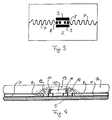
- the result in Fig. 3 is shown in the form of a plan view of the resulting circuit substrate, the film 1 is structured by photolithography or other suitable method so that it forms a conductor pattern with stretchable interconnects 7, which are each connected to a pad 8.
- An extensibility of the tracks 7 is achieved in that they are formed with a meandering or undulating course and thus have an excess length due to which they can be extended under tension without breakage.
- Reinforcing structures 9 which were formed during patterning from the conductive film 1 and stiffen the substrate layer and thus the resulting stretchable circuit carrier in an environment of the connection surfaces 8 can also be seen.
- the stiffening structures 9 are In this case, stiffening surfaces (stiffening pads) which are insulated from the conductor tracks 7 and the connection surfaces 8 and span a distance between the connection surfaces 8 without touching them, wherein the two connection surfaces 8 lie between two such stiffening pads.
- the conductor structure with a in the Fig. 4 recognizable electronic component 10 may be, which may be a sensor, an integrated circuit or a surface mounted device (SMD). It would be possible to mount this electronic component 10 in a manner known per se directly on the connection surfaces 8, for example by means of a conductive adhesive. In the present embodiment, however, the electronic component 10 is first attached to two additional surfaces which have been left standing in the patterning of the film 1, after which terminals 11 of the electronic component 10 by means of a conductive stretchable material 12, in the present example filled with conductive particles or fibers Plastic, are connected to the pads 8.
- a conductive stretchable material 12 in the present example filled with conductive particles or fibers Plastic
- the electronic component 10 is surrounded with another material 13, which is a polymer material which is poured over the electronic component 10 and after curing is stiffer than the stretchable substrate layer 5.
- another material 13 which is a polymer material which is poured over the electronic component 10 and after curing is stiffer than the stretchable substrate layer 5.
- a the electronic component 10 and the conductor structure with the conductor tracks 7 and the pads 8 overlapping second stretchable layer 14 applied which is again formed here of a thermoplastic polyurethane, which at a temperature of at most 130 ° C in liquefied form can be applied without destroying the electronic component 10 and its contacts.
- the starting material 3 used in the present example has a melting temperature of about 200 ° C, so that the stretchable substrate layer 5 does not flow when applying the second stretchable layer 14.
- an extensible circuit carrier has arisen, which can easily be extended several times to a length of approximately 150% of an initial length and can be relaxed again to the initial length.
- an expandable circuit carrier is produced comprising electronic components 10, thus forming an autonomous overall electronic system.
- Recurring features are in the FIGS. 5 to 8 again provided with the same reference numerals and have comparable properties, unless otherwise expressly stated.
- the film 1 is first provided by exposure to laser radiation 15 with position markings 16, which are given by depressions, as well as with orientation holes 17.
- This process step is in Fig. 5 illustrated.
- electronic components 10 which are present here in SMD design, are arranged with terminals 11 on the position markings 16 and thus also in a defined position relative to the orientation bores 17 on the conductive film 1 and connected in the present example by soldering to the film 1.
- the electronic components 10 instead, for example, by pressure welding, diffusion bonding or gluing be connected by means of a conductive adhesive to the film 1.
- the so connected to the film 1 electronic components 10 are then surrounded with a polymer material 13 and thereby fixed mechanically stable on the film 1.
- a stretchable substrate layer 5 which in this case has a thickness of about 100 .mu.m, wherein compared to this stretchable substrate layer 5, the material surrounding the electronic components 10 13 is stiffer.
- the film 1 now acts again in a conventional manner, so for example by photolithography, structured so that it forms a conductor structure with stretchable tracks 7 and pads 8, the orientation holes 15 serve as orientations in which the again meandering guided tracks 7 and the connection surfaces 8 are arranged in a defined position relative to the orientation bores 17.
- FIG. 1 illustrates a conductive stretchable material 12 which connects the terminals 11 of the electronic components 10 to the pads 8 and which could be applied locally prior to applying the stiffer material 13 or after structuring the film 1.
- second stretchable layer 14 is applied, after which the conductor structure is embedded in a now the stretchable substrate layer 5 and the second stretchable layer 14 comprehensive stretchable substrate.
- FIGS. 1 to 4 described method so with the basis of FIGS. 5 to 8 in the latter, before the second extensible layer 14 is applied, at least one further electronic component (10) is mounted on the conductor structure on a side of the film 1 facing away from the extensible substrate layer 5; Fig. 8 is shown with a dotted outline.
- an expandable circuit carrier which can be produced in the manner described can be shown, which can be, for example, an autonomous electronic system with sensor function for medical technology applications.
- the present invention thus proposes an advantageously simple method for producing a stretchable circuit substrate, in which a conductor structure is connected to a stretchable substrate layer, wherein the conductor pattern is formed such that it has extensible conductor tracks and terminal pads respectively connected to one of the extensible conductor tracks for at least an electronic component comprises.
- a preferred embodiment of the invention provides that a starting material for the substrate layer is applied to an electrically conductive film and connected to the film to form the expandable substrate layer, after which the Film is patterned so that it forms the conductor pattern, wherein also reinforcing structures are structured in the film, which stiffen the substrate layer in an environment of at least two pads without electrically connecting the pads together, thereby it is easy to prevent a electrical contact of a mounted on the pads electronic component in a stretching or relaxing the circuit substrate is damaged.
- a correspondingly advantageously expandable circuit carrier which can be produced by this method, comprises a stretchable substrate, a conductor structure embedded in the substrate or arranged on a surface of the substrate with stretchable interconnects and at least two connection surfaces respectively connected to one of the interconnects and at least one electronic component having terminals electrically conductively connected to the pads, the conductor pattern having in a plane with the tracks and formed of the same material as the tracks reinforcing structures stiffen the circuit carrier in an environment of the connected to the at least one electronic component pads, without connecting the pads electrically conductive together.
- circuit carrier is to be understood in such a way that it also includes - here stretchable - circuits that have in addition to a stretchable circuit board mounted or integrated electronic components.
Landscapes
- Engineering & Computer Science (AREA)
- Microelectronics & Electronic Packaging (AREA)
- Manufacturing & Machinery (AREA)
- Parts Printed On Printed Circuit Boards (AREA)
- Laminated Bodies (AREA)
- Electric Connection Of Electric Components To Printed Circuits (AREA)
Claims (19)
- Procédé de fabrication d'un support de circuit étirable, dans lequel un matériau de départ (3) est appliqué pour un substrat étirable sur un film électroconducteur (1), qui forme une couche de substrat étirable (5) reliée au film (1), le film (1) étant ensuite structuré de sorte qu'il forme une structure conductrice présentant au moins une piste conductrice étirable (7), caractérisé en ce que la structure conductrice comprend des surfaces de raccordement (8), qui sont reliées respectivement à une piste conductrice étirable (7) et des structures de renforcement (9) étant en outre intégrées dans le film (1), qui rigidifient la couche de substrat (5) autour d'au moins deux surfaces de raccordement (8) sans relier électriquement entre elles les surfaces de raccordement (8).
- Procédé selon la revendication 1, caractérisé en ce que l'au moins une piste conductrice (7) reçoit une forme incurvée alternativement dans des directions opposées entre elles à partir d'une direction principale de conducteur.
- Procédé selon l'une quelconque des revendications 1 ou 2, caractérisé en ce que le film conducteur (1) présente une épaisseur comprise entre 5 µm et 100 µm et/ou est fabriqué en cuivre, en argent ou en or.
- Procédé selon l'une quelconque des revendications 1 à 3, caractérisé en ce que le film (1) est rendu rugueux ou oxydée avant l'application du matériau de départ (3) sur une surface (2) orientée ultérieurement vers la couche de substrat étirable (5).
- Procédé selon l'une quelconque des revendications 1 à 4, caractérisé en ce que la couche de substrat étirable (5) est fabriquée en polyuréthane, en silicone, en caoutchouc ou en latex.
- Procédé selon l'une quelconque des revendications 1 à 5, caractérisé en ce que la couche de substrat étirable (5) présente une épaisseur comprise entre 25 µm et 1 mm.
- Procédé selon l'une quelconque des revendications 1 à 6, caractérisé en ce que le matériau de départ (3) est appliquée sur le film (1) par pression, raclage, moulage ou lainage.
- Procédé selon l'une quelconque des revendications 1 à 7, caractérisé en ce qu'une deuxième couche étirable (14) recouvrant la structure conductrice est appliquée après la structuration du film (1).
- Procédé selon l'une quelconque des revendications 1 à 8, caractérisé en ce que la structure conductrice est équipée, après la structuration du film (1), d'au moins un composant électronique (10).
- Procédé selon la revendication 9, caractérisé en ce que le composant électronique (10) est ensuite entouré d'un matériau (13) qui est plus rigide que la couche de substrat étirable (5).
- Procédé selon l'une quelconque des revendications 9 ou 10, dans la mesure ou elles se réfèrent à la revendication 8, caractérisé en ce que la deuxième couche étirable (14) est appliquée à une température plus basse que le matériau de départ (3) formant la couche de substrat étirable (5).
- Procédé selon l'une quelconque des revendications 1 à 8, caractérisé en ce que, avant l'application du matériau de départ (3) au moins un composant électronique (10) est disposé sur le film (1) et relié au film (1), l'au moins un composant électronique (10) étant encastré dans la couche de substrat étirable (5) se formant lors de l'application du matériau de départ (3).
- Procédé selon la revendication 12, caractérisé en ce que l'au moins un composant électronique (10) disposé sur le film (1) est entourée, avant l'application du matériau de départ (3), d'un matériau (13) qui est plus rigide que la couche de substrat étirable (5).
- Procédé selon l'une quelconque des revendications 12 ou 13, caractérisé en ce que le film (1) est muni, avant la disposition de l'au moins un composant électronique (10) sur le film (1), de marquages de positionnement (16) et/ou de perçages d'orientation (17), l'au moins un composant électronique (10) étant ensuite disposé au niveau des marquages de positionnement (16) et/ou dans une position définitive par rapport aux perçages d'orientation (17).
- Procédé selon l'une quelconque des revendications 9 à 14, caractérisé en ce que les raccordements (11) de l'au moins un composant électronique (10) sont reliés aux surfaces de raccordement (8) de la structure conductrice au moyen d'au moins un matériau conducteur étirable (12).
- Procédé selon l'une quelconque des revendications 9 à 15, caractérisé en ce que l'au moins un composant électrique (10) est soudé au film (1) ou à la structure conductrice.
- Support de circuit étirable comprenant un substrat étirable, une structure conductrice encastrée dans le substrat ou disposé sur une surface du substrat, présentant des pistes conductrices (7) et au moins deux surfaces de raccordement (8) reliées respectivement à l'une des pistes conductrices (7) ainsi qu'au moins un composant électronique (10) qui présente des raccordements (11) reliés de manière électro-conductrice aux surfaces de raccordement (8),
caractérisé en ce que
la structure conductrice présente des structures de renforcement (9) qui rigidifient le support de circuit autour des surfaces de raccordement (8) reliées à l'au moins un composant électronique (10) sans relier les surfaces de raccordement (8) de manière électro-conductrice entre elles. - Support de circuit étirable selon la revendication 17, caractérisé en ce que- l'au moins un composant électronique (10) est entouré d'un matériau (13) qui le relie mécaniquement à la structure conductrice et qui est plus rigide qu'un matériau formant le substrat étirable,et/ou- au moins un des raccordements (11) de l'au moins un composant électronique (10) est relié avec la surface de raccordement (8) correspondante au moyen d'un matériau conducteur étirable (12).
- Support de circuit étirable selon l'une quelconque des revendications 17 ou 18, pouvant être fabriqué selon l'une des revendications 1 à 16.
Applications Claiming Priority (1)
| Application Number | Priority Date | Filing Date | Title |
|---|---|---|---|
| DE102006055576A DE102006055576A1 (de) | 2006-11-21 | 2006-11-21 | Verfahren zum Herstellen eines dehnbaren Schaltungsträgers und dehnbarer Schaltungsträger |
Publications (3)
| Publication Number | Publication Date |
|---|---|
| EP1926355A2 EP1926355A2 (fr) | 2008-05-28 |
| EP1926355A3 EP1926355A3 (fr) | 2009-12-23 |
| EP1926355B1 true EP1926355B1 (fr) | 2014-01-08 |
Family
ID=39106123
Family Applications (1)
| Application Number | Title | Priority Date | Filing Date |
|---|---|---|---|
| EP07076013.7A Ceased EP1926355B1 (fr) | 2006-11-21 | 2007-11-21 | Procédé de fabrication d'un support de circuit extensible et support de circuit extensible |
Country Status (3)
| Country | Link |
|---|---|
| US (1) | US8654536B2 (fr) |
| EP (1) | EP1926355B1 (fr) |
| DE (1) | DE102006055576A1 (fr) |
Cited By (1)
| Publication number | Priority date | Publication date | Assignee | Title |
|---|---|---|---|---|
| DE102024210035A1 (de) | 2024-10-16 | 2026-04-16 | Fraunhofer-Gesellschaft zur Förderung der angewandten Forschung eingetragener Verein | Verfahren zur Herstellung eines Transportmittels mit einem Substrat und einer Leiterstruktur |
Families Citing this family (35)
| Publication number | Priority date | Publication date | Assignee | Title |
|---|---|---|---|---|
| DE102008002532A1 (de) | 2008-06-19 | 2009-12-24 | Robert Bosch Gmbh | Verfahren zur Herstellung einer elektronischen Baugruppe |
| EP2392198B1 (fr) * | 2009-01-30 | 2018-08-22 | IMEC vzw | Dispositif électronique extensible et son procédé de fabrication |
| EP2392196B1 (fr) * | 2009-01-30 | 2018-08-22 | IMEC vzw | Dispositif électronique extensible |
| DE102009016368A1 (de) * | 2009-04-07 | 2010-10-21 | Carl Freudenberg Kg | Schaltungsträger mit elektrischen Leiterbahnen |
| WO2010146524A1 (fr) * | 2009-06-19 | 2010-12-23 | Koninklijke Philips Electronics N.V. | Dispositifs électroniques conformables, et leurs procédés de fabrication |
| DE102009031568A1 (de) * | 2009-06-29 | 2010-12-30 | Fraunhofer-Gesellschaft zur Förderung der angewandten Forschung e.V. | Verfahren zur Erzeugung eines elektronischen Systems, Verfahren zur Erzeugung einer Freiformfläche mit einem solchen System, sowie elektronisches System und Freiformflächen mit einem solchen System |
| DE102009031600A1 (de) * | 2009-07-07 | 2011-01-13 | Fraunhofer-Gesellschaft zur Förderung der angewandten Forschung e.V. | Photovoltaikmodul und Verfahren zur Herstellung eines Photovoltaikmoduls |
| EP2355144A1 (fr) | 2010-02-09 | 2011-08-10 | Nederlandse Organisatie voor toegepast -natuurwetenschappelijk onderzoek TNO | Placement des composants sur des substrats souples et/ou étirables |
| DE102010034718B4 (de) | 2010-08-18 | 2017-11-30 | Deutsches Zentrum für Luft- und Raumfahrt e.V. | Dehnbares Substrat mit einer Kontaktstelle zwischen einem polymerbasierten elektrischen Leiter und einem weiteren elektrischen Leiter |
| EP2461658A1 (fr) | 2010-12-03 | 2012-06-06 | Nederlandse Organisatie voor toegepast -natuurwetenschappelijk onderzoek TNO | Procédé et appareil pour assembler des composants électriques sur un substrat flexible ainsi que l'assemblage d'un composant électrique avec un substrat flexible |
| GB2529346A (en) | 2011-03-31 | 2016-02-17 | Plasyl Ltd | Improvements for electrical circuits |
| USD701182S1 (en) | 2011-04-12 | 2014-03-18 | Plasyl Limited | Wave circuit pattern |
| US9247637B2 (en) * | 2012-06-11 | 2016-01-26 | Mc10, Inc. | Strain relief structures for stretchable interconnects |
| US9226402B2 (en) * | 2012-06-11 | 2015-12-29 | Mc10, Inc. | Strain isolation structures for stretchable electronics |
| DE102013019723A1 (de) | 2012-12-12 | 2014-06-12 | Carl Freudenberg Kg | Dünnes Leuchtelement |
| JP6518451B2 (ja) * | 2015-02-02 | 2019-05-22 | 株式会社フジクラ | 伸縮性回路基板 |
| CN107210269B (zh) * | 2015-03-11 | 2020-07-28 | 英特尔公司 | 利用应变重分布层的可拉伸电子器件制造方法 |
| US9572261B2 (en) * | 2015-03-25 | 2017-02-14 | Texas Instruments Incorporated | Conductive through-polymer vias for capacitative structures integrated with packaged semiconductor chips |
| WO2017017127A1 (fr) | 2015-07-28 | 2017-02-02 | At & S Austria Technologie & Systemtechnik Aktiengesellschaft | Support étirable de composants électroniques |
| US9683132B2 (en) | 2015-09-11 | 2017-06-20 | Advanced Consulting Technologies, Inc. | Process for protecting an electronic device by selective deposition of polymer coatings |
| US20190045627A1 (en) * | 2015-09-17 | 2019-02-07 | Sekisui Polymatech Co., Ltd. | Elastic Wiring Member |
| DE112015006957T5 (de) * | 2015-09-24 | 2018-06-07 | Intel Corporation | Dehnbare elektronische Anordnung |
| FI20165054A (fi) * | 2016-01-28 | 2017-07-29 | Clothing Plus Mbu Oy | Joustava piirilevy |
| JP2018014381A (ja) * | 2016-07-20 | 2018-01-25 | 富士通株式会社 | 基板及び電子機器 |
| US20180061578A1 (en) * | 2016-09-01 | 2018-03-01 | Apple Inc. | Stacked passive component structures |
| JP6972523B2 (ja) * | 2016-09-13 | 2021-11-24 | セイコーエプソン株式会社 | 電子機器 |
| JP6776840B2 (ja) | 2016-11-21 | 2020-10-28 | オムロン株式会社 | 電子装置およびその製造方法 |
| WO2018168734A1 (fr) * | 2017-03-13 | 2018-09-20 | 株式会社村田製作所 | Structure de résine à composant électronique intégré et son procédé de production |
| JP6903981B2 (ja) * | 2017-03-23 | 2021-07-14 | セイコーエプソン株式会社 | 検出装置 |
| US20200132520A1 (en) * | 2017-07-14 | 2020-04-30 | Sony Corporation | Sensor and method of manufacturing sensor |
| FI20175818A1 (en) * | 2017-09-14 | 2019-03-15 | Clothing Plus Mbu Oy | Electrical signal transmission system |
| WO2020195544A1 (fr) * | 2019-03-25 | 2020-10-01 | 株式会社村田製作所 | Substrat monté élastique |
| TW202214065A (zh) * | 2020-08-07 | 2022-04-01 | 日商昭和電工材料股份有限公司 | 零件內建基板之製造方法及零件內建基板 |
| AT526502B1 (de) * | 2023-03-23 | 2024-04-15 | Sendance Gmbh | Verformbarer Gegenstand |
| DE102023113352A1 (de) * | 2023-05-22 | 2024-11-28 | Deutsches Zentrum für Luft- und Raumfahrt e.V. | Verfahren und Sensorvorrichtung zur Erfassung von Schwingungen ausgedehnter balkenartiger Systeme |
Family Cites Families (13)
| Publication number | Priority date | Publication date | Assignee | Title |
|---|---|---|---|---|
| DE3019207A1 (de) * | 1980-05-20 | 1981-11-26 | GAO Gesellschaft für Automation und Organisation mbH, 8000 München | Traegerelement fuer einen ic-chip |
| FR2673017A1 (fr) * | 1991-02-18 | 1992-08-21 | Schlumberger Ind Sa | Procede de fabrication d'un module electronique pour carte a memoire et module electronique ainsi obtenu. |
| JPH06314877A (ja) * | 1993-04-30 | 1994-11-08 | Mitsui Toatsu Chem Inc | 長尺状両面フレキシブル金属積層板の製造方法 |
| DE4410732C2 (de) * | 1994-03-28 | 1997-05-07 | Amatech Gmbh & Co Kg | Verfahren zur Anordnung einer zumindest einen Chip und eine Drahtspule aufweisenden Transpondereinheit auf einem Substrat sowie Chipkarte mit entsprechend angeordneter Transpondereinheit |
| US6654064B2 (en) * | 1997-05-23 | 2003-11-25 | Canon Kabushiki Kaisha | Image pickup device incorporating a position defining member |
| US6404643B1 (en) * | 1998-10-15 | 2002-06-11 | Amerasia International Technology, Inc. | Article having an embedded electronic device, and method of making same |
| US6606247B2 (en) * | 2001-05-31 | 2003-08-12 | Alien Technology Corporation | Multi-feature-size electronic structures |
| US7265298B2 (en) * | 2003-05-30 | 2007-09-04 | The Regents Of The University Of California | Serpentine and corduroy circuits to enhance the stretchability of a stretchable electronic device |
| TWI321975B (en) * | 2003-06-27 | 2010-03-11 | Ajinomoto Kk | Resin composition and adhesive film for multi-layered printed wiring board |
| DE20320760U1 (de) * | 2003-09-25 | 2005-03-10 | Ruwel Ag | Basiselement für flexible oder semi-flexible ein- oder mehrlagige gedruckte Schaltungen |
| DE102004030140B3 (de) * | 2004-06-22 | 2006-01-19 | Infineon Technologies Ag | Flexible Kontaktierungsvorrichtung |
| GB0505826D0 (en) * | 2005-03-22 | 2005-04-27 | Uni Microelektronica Ct Vsw | Methods for embedding of conducting material and devices resulting from said methods |
| KR100716826B1 (ko) * | 2005-05-10 | 2007-05-09 | 삼성전기주식회사 | 전자부품이 내장된 기판의 제조방법 |
-
2006
- 2006-11-21 DE DE102006055576A patent/DE102006055576A1/de not_active Ceased
-
2007
- 2007-11-15 US US11/940,640 patent/US8654536B2/en not_active Expired - Fee Related
- 2007-11-21 EP EP07076013.7A patent/EP1926355B1/fr not_active Ceased
Cited By (2)
| Publication number | Priority date | Publication date | Assignee | Title |
|---|---|---|---|---|
| DE102024210035A1 (de) | 2024-10-16 | 2026-04-16 | Fraunhofer-Gesellschaft zur Förderung der angewandten Forschung eingetragener Verein | Verfahren zur Herstellung eines Transportmittels mit einem Substrat und einer Leiterstruktur |
| DE102024210035B4 (de) | 2024-10-16 | 2026-05-07 | Fraunhofer-Gesellschaft zur Förderung der angewandten Forschung eingetragener Verein | Verfahren zur Herstellung eines Transportmittels mit einem Substrat und einer Leiterstruktur |
Also Published As
| Publication number | Publication date |
|---|---|
| US20080257589A1 (en) | 2008-10-23 |
| US8654536B2 (en) | 2014-02-18 |
| EP1926355A2 (fr) | 2008-05-28 |
| DE102006055576A1 (de) | 2008-05-29 |
| EP1926355A3 (fr) | 2009-12-23 |
Similar Documents
| Publication | Publication Date | Title |
|---|---|---|
| EP1926355B1 (fr) | Procédé de fabrication d'un support de circuit extensible et support de circuit extensible | |
| EP2027600B1 (fr) | Procédé pour noyer au moins un composant dans un élément de carte de circuits imprimés | |
| DE102010042567B3 (de) | Verfahren zum Herstellen eines Chip-Package und Chip-Package | |
| EP2545598B1 (fr) | Transducteur de flexion | |
| DE60300619T2 (de) | Verfahren zum einbetten einer komponente in eine basis und zur bildung eines kontakts | |
| DE102005047856B4 (de) | Halbleiterbauteil mit in Kunststoffgehäusemasse eingebetteten Halbleiterbauteilkomponenten, Systemträger zur Aufnahme der Halbleiterbauteilkomponenten und Verfahren zur Herstellung des Systemträgers und von Halbleiterbauteilen | |
| EP2668835B1 (fr) | Procédé d'intégration d'un composant électronique dans une carte à circuit imprimé ou un produit intermédiaire de carte à circuit imprimé | |
| EP1394855B1 (fr) | Procédé de fabrication d'un boîtier universel pour dispositif électronique semi-conducteur | |
| WO2001075969A1 (fr) | Composant electronique pourvu de points de contact flexibles, et son procede de fonctionnement | |
| DE102008047416A1 (de) | Halbleiteranordnung und Verfahren zur Herstelllung von Halbleiteranordnungen | |
| EP2852970B1 (fr) | Procédé de fabrication d'un module électronique | |
| DE102014101366B3 (de) | Chip-Montage an über Chip hinausstehender Adhäsions- bzw. Dielektrikumsschicht auf Substrat | |
| WO2010028884A2 (fr) | Encapsulage, système micro-électromécanique et procédé d'encapsulage | |
| WO2013013964A1 (fr) | Dispositif support, dispositif électrique pourvu d'un dispositif support, et procédé de fabrication de ces dispositifs | |
| DE60133429T2 (de) | Verdrahtungssubstrat, seine Herstellung und Halbleiterbauteil | |
| DE102019202715A1 (de) | Folienbasiertes package mit distanzausgleich | |
| EP0841668B1 (fr) | Résistance électrique et son procédé de fabrication | |
| WO2008104324A1 (fr) | Procédé d'intégration de puces dans des cavités de cartes à circuit imprimé | |
| WO2014161020A1 (fr) | Procédé de fabrication d'un élément de circuit imprimé | |
| DE102009040627B4 (de) | Halbleiterbauelement und Verfahren zum Herstellen eines elektronischen Systems | |
| DE102013104567A1 (de) | Chipanordnung, Chipkartenanordnung und Verfahren zum Herstellen einer Chipanordnung | |
| DE10210841B4 (de) | Modul und Verfahren zur Herstellung von elektrischen Schaltungen und Modulen | |
| WO2017088998A1 (fr) | Élément électrique avec une couche mince d'arrêt de soudure et son procédé de fabrication | |
| DE102010064453B4 (de) | Verfahren zum Herstellen eines Chip-Package | |
| DE3601151A1 (de) | Verfahren zur herstellung von montagestreifen fuer die automatische montage integrierter schaltungen und nach dem verfahren hergestellter montagestreifen |
Legal Events
| Date | Code | Title | Description |
|---|---|---|---|
| PUAI | Public reference made under article 153(3) epc to a published international application that has entered the european phase |
Free format text: ORIGINAL CODE: 0009012 |
|
| AK | Designated contracting states |
Kind code of ref document: A2 Designated state(s): AT BE BG CH CY CZ DE DK EE ES FI FR GB GR HU IE IS IT LI LT LU LV MC MT NL PL PT RO SE SI SK TR |
|
| AX | Request for extension of the european patent |
Extension state: AL BA HR MK RS |
|
| RIN1 | Information on inventor provided before grant (corrected) |
Inventor name: PATZELT, RAINER Inventor name: MANESSIS, DIONYSIOS Inventor name: SECKEL, MANUEL Inventor name: LOEHER, THOMAS Inventor name: OSTMANN, ANDREAS |
|
| PUAL | Search report despatched |
Free format text: ORIGINAL CODE: 0009013 |
|
| AK | Designated contracting states |
Kind code of ref document: A3 Designated state(s): AT BE BG CH CY CZ DE DK EE ES FI FR GB GR HU IE IS IT LI LT LU LV MC MT NL PL PT RO SE SI SK TR |
|
| AX | Request for extension of the european patent |
Extension state: AL BA HR MK RS |
|
| 17P | Request for examination filed |
Effective date: 20100623 |
|
| 17Q | First examination report despatched |
Effective date: 20100726 |
|
| AKX | Designation fees paid |
Designated state(s): DE FR GB |
|
| GRAP | Despatch of communication of intention to grant a patent |
Free format text: ORIGINAL CODE: EPIDOSNIGR1 |
|
| INTG | Intention to grant announced |
Effective date: 20130813 |
|
| RIN1 | Information on inventor provided before grant (corrected) |
Inventor name: PATZELT, RAINER Inventor name: OSTMANN, ANDREAS Inventor name: SECKEL, MANUEL Inventor name: MANESSIS, DIONYSIOS Inventor name: LOEHER, THOMAS |
|
| GRAS | Grant fee paid |
Free format text: ORIGINAL CODE: EPIDOSNIGR3 |
|
| GRAA | (expected) grant |
Free format text: ORIGINAL CODE: 0009210 |
|
| AK | Designated contracting states |
Kind code of ref document: B1 Designated state(s): DE FR GB |
|
| REG | Reference to a national code |
Ref country code: GB Ref legal event code: FG4D Free format text: NOT ENGLISH |
|
| REG | Reference to a national code |
Ref country code: DE Ref legal event code: R096 Ref document number: 502007012672 Country of ref document: DE Effective date: 20140220 |
|
| REG | Reference to a national code |
Ref country code: DE Ref legal event code: R097 Ref document number: 502007012672 Country of ref document: DE |
|
| PLBE | No opposition filed within time limit |
Free format text: ORIGINAL CODE: 0009261 |
|
| STAA | Information on the status of an ep patent application or granted ep patent |
Free format text: STATUS: NO OPPOSITION FILED WITHIN TIME LIMIT |
|
| 26N | No opposition filed |
Effective date: 20141009 |
|
| REG | Reference to a national code |
Ref country code: DE Ref legal event code: R097 Ref document number: 502007012672 Country of ref document: DE Effective date: 20141009 |
|
| REG | Reference to a national code |
Ref country code: FR Ref legal event code: PLFP Year of fee payment: 9 |
|
| REG | Reference to a national code |
Ref country code: FR Ref legal event code: PLFP Year of fee payment: 10 |
|
| REG | Reference to a national code |
Ref country code: FR Ref legal event code: PLFP Year of fee payment: 11 |
|
| P01 | Opt-out of the competence of the unified patent court (upc) registered |
Effective date: 20230524 |
|
| PGFP | Annual fee paid to national office [announced via postgrant information from national office to epo] |
Ref country code: GB Payment date: 20231123 Year of fee payment: 17 |
|
| PGFP | Annual fee paid to national office [announced via postgrant information from national office to epo] |
Ref country code: FR Payment date: 20231124 Year of fee payment: 17 Ref country code: DE Payment date: 20231120 Year of fee payment: 17 |
|
| REG | Reference to a national code |
Ref country code: DE Ref legal event code: R119 Ref document number: 502007012672 Country of ref document: DE |
|
| GBPC | Gb: european patent ceased through non-payment of renewal fee |
Effective date: 20241121 |
|
| PG25 | Lapsed in a contracting state [announced via postgrant information from national office to epo] |
Ref country code: DE Free format text: LAPSE BECAUSE OF NON-PAYMENT OF DUE FEES Effective date: 20250603 |
|
| PG25 | Lapsed in a contracting state [announced via postgrant information from national office to epo] |
Ref country code: GB Free format text: LAPSE BECAUSE OF NON-PAYMENT OF DUE FEES Effective date: 20241121 |
|
| PG25 | Lapsed in a contracting state [announced via postgrant information from national office to epo] |
Ref country code: FR Free format text: LAPSE BECAUSE OF NON-PAYMENT OF DUE FEES Effective date: 20241130 |