EP1928014A2 - Ladungsfallenschicht für eine Ladungsfallen-Halbleiterspeichervorrichtung und Herstellungsverfahren dafür - Google Patents
Ladungsfallenschicht für eine Ladungsfallen-Halbleiterspeichervorrichtung und Herstellungsverfahren dafür Download PDFInfo
- Publication number
- EP1928014A2 EP1928014A2 EP07121684A EP07121684A EP1928014A2 EP 1928014 A2 EP1928014 A2 EP 1928014A2 EP 07121684 A EP07121684 A EP 07121684A EP 07121684 A EP07121684 A EP 07121684A EP 1928014 A2 EP1928014 A2 EP 1928014A2
- Authority
- EP
- European Patent Office
- Prior art keywords
- layer
- charge trap
- precursor material
- precursor
- memory device
- Prior art date
- Legal status (The legal status is an assumption and is not a legal conclusion. Google has not performed a legal analysis and makes no representation as to the accuracy of the status listed.)
- Withdrawn
Links
Images


Classifications
-
- H—ELECTRICITY
- H10—SEMICONDUCTOR DEVICES; ELECTRIC SOLID-STATE DEVICES NOT OTHERWISE PROVIDED FOR
- H10P—GENERIC PROCESSES OR APPARATUS FOR THE MANUFACTURE OR TREATMENT OF DEVICES COVERED BY CLASS H10
- H10P14/00—Formation of materials, e.g. in the shape of layers or pillars
- H10P14/60—Formation of materials, e.g. in the shape of layers or pillars of insulating materials
- H10P14/63—Formation of materials, e.g. in the shape of layers or pillars of insulating materials characterised by the formation processes
- H10P14/6302—Non-deposition formation processes
- H10P14/6304—Formation by oxidation, e.g. oxidation of the substrate
-
- H—ELECTRICITY
- H10—SEMICONDUCTOR DEVICES; ELECTRIC SOLID-STATE DEVICES NOT OTHERWISE PROVIDED FOR
- H10D—INORGANIC ELECTRIC SEMICONDUCTOR DEVICES
- H10D30/00—Field-effect transistors [FET]
- H10D30/60—Insulated-gate field-effect transistors [IGFET]
- H10D30/68—Floating-gate IGFETs
- H10D30/681—Floating-gate IGFETs having only two programming levels
- H10D30/683—Floating-gate IGFETs having only two programming levels programmed by tunnelling of carriers, e.g. Fowler-Nordheim tunnelling
-
- H—ELECTRICITY
- H10—SEMICONDUCTOR DEVICES; ELECTRIC SOLID-STATE DEVICES NOT OTHERWISE PROVIDED FOR
- H10D—INORGANIC ELECTRIC SEMICONDUCTOR DEVICES
- H10D30/00—Field-effect transistors [FET]
- H10D30/60—Insulated-gate field-effect transistors [IGFET]
- H10D30/68—Floating-gate IGFETs
- H10D30/6891—Floating-gate IGFETs characterised by the shapes, relative sizes or dispositions of the floating gate electrode
-
- H—ELECTRICITY
- H10—SEMICONDUCTOR DEVICES; ELECTRIC SOLID-STATE DEVICES NOT OTHERWISE PROVIDED FOR
- H10D—INORGANIC ELECTRIC SEMICONDUCTOR DEVICES
- H10D30/00—Field-effect transistors [FET]
- H10D30/60—Insulated-gate field-effect transistors [IGFET]
- H10D30/69—IGFETs having charge trapping gate insulators, e.g. MNOS transistors
- H10D30/694—IGFETs having charge trapping gate insulators, e.g. MNOS transistors characterised by the shapes, relative sizes or dispositions of the gate electrodes
-
- H—ELECTRICITY
- H10—SEMICONDUCTOR DEVICES; ELECTRIC SOLID-STATE DEVICES NOT OTHERWISE PROVIDED FOR
- H10D—INORGANIC ELECTRIC SEMICONDUCTOR DEVICES
- H10D64/00—Electrodes of devices having potential barriers
- H10D64/01—Manufacture or treatment
- H10D64/031—Manufacture or treatment of data-storage electrodes
- H10D64/035—Manufacture or treatment of data-storage electrodes comprising conductor-insulator-conductor-insulator-semiconductor structures
-
- H—ELECTRICITY
- H10—SEMICONDUCTOR DEVICES; ELECTRIC SOLID-STATE DEVICES NOT OTHERWISE PROVIDED FOR
- H10D—INORGANIC ELECTRIC SEMICONDUCTOR DEVICES
- H10D64/00—Electrodes of devices having potential barriers
- H10D64/01—Manufacture or treatment
- H10D64/031—Manufacture or treatment of data-storage electrodes
- H10D64/037—Manufacture or treatment of data-storage electrodes comprising charge-trapping insulators
-
- Y—GENERAL TAGGING OF NEW TECHNOLOGICAL DEVELOPMENTS; GENERAL TAGGING OF CROSS-SECTIONAL TECHNOLOGIES SPANNING OVER SEVERAL SECTIONS OF THE IPC; TECHNICAL SUBJECTS COVERED BY FORMER USPC CROSS-REFERENCE ART COLLECTIONS [XRACs] AND DIGESTS
- Y10—TECHNICAL SUBJECTS COVERED BY FORMER USPC
- Y10T—TECHNICAL SUBJECTS COVERED BY FORMER US CLASSIFICATION
- Y10T428/00—Stock material or miscellaneous articles
- Y10T428/31504—Composite [nonstructural laminate]
- Y10T428/31678—Of metal
Definitions
- a non-volatile memory device is a storage device that may maintain previously stored data even when the power is turned off.
- the structure of memory cells constituting the non-volatile memory device may vary according to the field where the non-volatile memory device is used.
- a gate of a transistor thereof may include a floating gate in which charges (e.g., data), are stored, and a control gate controlling the floating gate may be sequentially stacked.
- the size of memory cells may be rapidly reduced in the flash semiconductor memory device. Also, it may be desirable to reduce the height of the floating gate in a vertical direction according to the reduction in the size of the memory cells.
- a semiconductor memory device having a silicon-oxide-nitride-oxide-semiconductor (SONOS) structure or a metal-oxide-insulator-oxide-semiconductor (MOIOS) structure (such as a metal-oxide-nitride-oxide-semiconductor (MONOS)), which are formed of a silicon nitride layer (Si 3 N 4 ) instead of a floating gate as a means for storing charges, has been suggested and actively researched.
- the SONOS memory device may use silicon as a material for the control gate, and the MONOS memory device may use metal for a material for the control gate.
- the SONOS memory device is disclosed in more detail in " An Embedded 90nm SONOS Nonvolatile Memory Utilizing Hot Electron Programming and Uniform Tunnel Erase” by C.T. Swift et al., on p. 927-930 in Technical Digest of International Electron Device Meeting (IEDM published in December, 2002 ).
- the SONOS memory device may have a first silicon oxide layer (SiO 2 ) formed as a tunnel insulating layer such that both ends of the silicon oxide layer may contact source and drain regions on a semiconductor substrate between the source and drain regions (e.g., on a channel region).
- the first silicon oxide layer may be for tunneling of charges.
- a silicon nitride layer (Si 3 N 4 ) may be formed on the first silicon oxide layer as a charge trap layer.
- the silicon nitride layer may be a material layer in which data is substantially stored and charges which have passed through the first silicon oxide layer are trapped in the silicon nitride layer, for example.
- a second silicon oxide layer may be formed on the silicon nitride layer to block charges that pass through the silicon nitride layer and move upward.
- a gate electrode may be formed on the second silicon oxide layer.
- the SONOS memory device having the above structure may have problems in that the permittivity of the silicon nitride layer and the silicon oxide layer is lower and the density of the trap site in the silicon nitride layer may not be sufficient.
- the operation voltage may be higher, and the data recording speed (programming speed) and the charge retention time in vertical and horizontal directions may not be as desired.
- the blocking insulating layer formed of an aluminum oxide may suppress charges that go out from the silicon nitride layer, the trap site density in the silicon nitride layer itself may still not be sufficient. Thus, the retention characteristic may not be improved by using an aluminum oxide layer.
- U.S. Patent Publication No. 2004/0264236 A1 discloses a memory device which may be realized by using an insulating thin film of HfO 2 including a lanthanide metal impurity instead of a silicon nitride layer as a charge trap material.
- U.S. Patent No. 6,998,317 discloses a memory device including a charge trap layer that may be formed by stacking an HfO 2 insulating thin film and treating the same with plasma.
- a memory device including a charge trap layer which may be formed by forming a nanolaminate thin film of HfO 2 and Al 2 O 3 thin films using an atom layer deposition (ALD) method as a charge trap material is disclosed in " High density and program-erasable metal-insulator-silicon capacitor with a dielectric structure of SiO2/HfO2-Al2O3 nanolaminate/Al2O3" by Shi-Jin Ding et al., pp. 0429051-0429053 in Applied Physics Letter vol. 88, published in 2006 .
- ALD atom layer deposition
- a metal impurity such as lanthanide metal as disclosed in U.S. Patent Publication No. 2004/0264236 A1
- an insulating thin film used as a layer to trap and maintain charges e.g., used as a charge trap layer, or a defect in HfO 2 thin film which may be induced by plasma as disclosed in U.S. Patent No. 6,998,317
- the defect or the metal impurity which is a charge trap site
- the horizontal and vertical distance between trap sites may not be controlled as desired.
- the defect of the HfO 2 layer in the nanolaminate thin films stacked in the HfO 2 and Al 2 O 3 thin films or the defect of the interface defect between the HfO 2 and Al 2 O 3 thin films may act as a charge trap site.
- the density of trap site may determine the programming and retention characteristics. To increase the programming speed, the density of trap site may need to be effectively increased. Because the nanolaminate thin films may use the defect in the HfO 2 thin film or the defect of the interface, it may be difficult to increase the density of trap site.
- Example embodiments may provide a charge trap semiconductor memory device that may include a thin layer of a high-k dielectric insulator containing a metal impurity, the position of which is controlled, (e.g., site-modulated, metal-doped insulator SMI) as a charge trap layer, and a method of manufacturing the charge trap semiconductor memory device.
- a charge trap semiconductor memory device may include a thin layer of a high-k dielectric insulator containing a metal impurity, the position of which is controlled, (e.g., site-modulated, metal-doped insulator SMI) as a charge trap layer, and a method of manufacturing the charge trap semiconductor memory device.
- a charge trap semiconductor memory device may include a thin layer of a high-k dielectric insulator containing a metal impurity, the position of which is controlled, (e.g., site-modulated, metal-doped insulator SMI) as a charge trap layer, and a method of manufacturing the charge trap semiconductor memory
- a method of manufacturing a charge trap layer including (a) coating a first precursor material on a surface of a semiconductor substrate and oxidizing the first precursor material to form a first layer formed of an insulating material; (b) coating a second precursor material formed of metallicity on the first layer; (c) supplying the first precursor material on the surface coated with the second precursor material to substitute the second precursor material with the first precursor material; and (d) oxidizing the first and second precursor materials obtained in (c) to form a second layer formed of an insulating material and a metal impurity.
- the method may be performed at least one time to form a charge trap layer having a structure in which the metal impurity is isolated in the insulating material.
- the operation (a) may be performed at least one time.
- the coating of the first precursor material and the supplying of an oxidizer for oxidizing the first precursor material may be performed sequentially.
- the first and second precursor materials may be coated by spilling the first and second precursor materials to saturate a surface with the molecules of the first and second precursor materials.
- the example method may also include purging to remove a remaining gas and reaction residual product after coating the first or second precursor material.
- the first precursor material may be a metal precursor, such as trimethylauminum (TMA) and the insulating material may be Al 2 O 3, for example.
- TMA trimethylauminum
- the second precursor material may be diethylzinc, and the charge trap layer may be formed of a Zn-doped Al 2 O 3 .
- H 2 O may be used as an oxidizer for oxidizing the first and second precursor materials.
- a charge trap semiconductor memory device including a tunnel insulating layer formed on a semiconductor substrate, and a charge trap layer formed on the tunnel insulating layer.
- the charge trap layer may have a first layer formed of an insulating layer, and a second layer formed of the same insulating layer as the first layer and a metal impurity that may be isolated in the insulating material on a molecular level.
- the charge trap semiconductor memory device may include at least one pair of the first and second layers.
- the second layer may be formed of one layer and the first layer is formed of at least one layer.
- the first and second layers may be formed in atom layer unit.
- the charge trap layer may be formed of Zn-doped Al 2 O 3 .
- FIG. 1 is a schematic view of a charge trap semiconductor memory device 10 according to an embodiment of the present invention.
- the thicknesses of layers and regions in FIG. 1 are exaggerated for clarity.
- the charge trap semiconductor memory device 10 may include a gate stack 20 formed on a semiconductor substrate 10.
- First and second impurity regions 13 and 15 doped with a predetermined conductive impurity may be formed on the semiconductor substrate 11.
- One of the first and second impurity regions 13 and 15 may be a drain region (D) and the other one thereof may be a source region (S).
- the gate stack 20 may be formed to be in contact with the first and second impurity regions 13 and 15.
- the gate stack 20 may include a charge trap layer 23.
- a tunnel insulating layer 21 may be formed between the semiconductor substrate 11 and the charge trap layer 23.
- the tunnel insulating layer 21 may be formed on the semiconductor substrate 11 to be in contact with the first and second impurity regions 13 and 15.
- a blocking insulating layer 25 may be formed on the charge trap layer 23, and a gate electrode 27 may be formed on the blocking insulating layer 25.
- the tunnel insulating layer 21, the charge trap layer 23, the blocking insulating layer 25, and the gate electrode 27 may be sequentially stacked on the semiconductor substrate 11.
- the thickness of the tunnel insulating layer 21 may be 1.5 to 5 nm.
- the tunnel insulating layer 21 may be formed of an insulating thin film, such as a silicon oxide layer (SiO 2 ), a silicon nitride layer (Si 3 N 4 ), a silicon oxide-nitride-layer (SiO x N y ) or an aluminum oxide layer (Al 2 O 3 ) using a thermal oxidization method, a chemical vapor deposition (CVD) method, or an atom layer deposition (ALD) method, for example.
- a silicon oxide layer SiO 2
- Si 3 N 4 silicon nitride layer
- SiO x N y silicon oxide-nitride-layer
- Al 2 O 3 aluminum oxide layer
- the charge trap layer 23 may be formed of a thin layer of a high-k dielectric insulator containing a metal impurity of which the position is controlled (e.g., a site-modulated metal-doped insulator (SMI)).
- the charge trap layer 23 may be formed such that the metal impurity may be isolated at a molecular level in the insulating thin film.
- the charge trap layer 23 may be formed such that ZnO may be isolated at a molecular level in an Al 2 O 3 layer.
- the charge trap layer 23 may be formed to a thickness of 2 to 15 nm using an ALD method, for example.
- the ALD method is a modified method of a chemical vapor deposition (CVD) method in order to induce self-limiting growth of a thin film.
- CVD chemical vapor deposition
- a metal precursor and an oxidization gas to be deposited as a thin layer may be supplied to a deposition apparatus at the same time forming a thin film by pyrolysis and oxidization.
- a metal precursor and an oxygen gas may be sequentially supplied between supplying the metal precursor and the oxygen, purging may be performed to remove a remaining gas and a reaction residual product from a reactor using an inactive gas such as Ar.
- the processes may be performed at 200 to 300°C at which the precursors may not be pyrolysed. Accordingly, the thin film may be formed by controlling in an atom layer unit by only the adhesion reaction on the surface.
- the blocking insulating layer 25 may be formed of a high-k dielectric thin film having a high permittivity and band gap.
- the blocking insulating layer 25 may be formed of Si 3 N4, HfO 2 , Ta 2 O 5 , ZrO 2 , or Al 2 O 3 layer.
- the gate electrode 27 may be formed of a metal layer having an increased work function.
- the gate electrode 27 may be formed of gold (Au) or an aluminum layer.
- the gate electrode 27 may be formed of a metal such as Ru or TaN, or a silicide material such as NiSi that is used usually as a gate electrode of a semiconductor memory device, for example.
- the charge trap layer 23 ay be formed of an insulating material containing a metal impurity, such as Al 2 O 3 layer containing Zn.
- a first precursor may be applied to a surface of a substrate 31 to be deposited, for example, on a surface of a semiconductor substrate 11 on which a tunnel insulating layer 21 may be formed.
- the first precursor may be used to saturate the surface of the substrate 31 with a molecule 33' of the first precursor material.
- the first precursor material may be provided as plasma, for example.
- a metal precursor may be used as the first precursor material.
- the first precursor material may be an Al precursor (e.g., trimethylaluminum (TMA)).
- TMA trimethylaluminum
- the TMA molecule saturated on the surface of the substrate may be oxidized by supplying oxidization gas.
- the saturated TMA molecule may be oxidized using H 2 O, which is an oxidizer, to form a first layer 33 formed of an Al 2 O 3 thin film.
- a second precursor material of metallicity may be applied to the surface of the first layer 33 to saturate the surfaces of the first layer 33 with a molecule 35' of the second precursor material, as illustrated in FIG. 2C .
- the second precursor material may be provided as plasma, for example.
- the second precursor material may be a Zn precursor, (e.g., diethylzinc (DEZ)).
- DEZ diethylzinc
- the second precursor material will be represented as DEZ.
- D denotes a monomer of a DEZ molecule.
- a portion of the DEZ molecule 35' may be substituted with a TMA molecule 35" by applying a TMA molecule, as illustrated in FIG. 2D .
- the portion by saturated DEZ and TMA molecules 35' and 35" are oxidized by applying H 2 O thereon. Then, a second layer 35 which is a thin film, in which a metal impurity 35a (ZnO) may be isolated inside an insulating material 35b (Al 2 O 3 ) at a molecular level, is obtained.
- a metal impurity 35a ZnO
- insulating material 35b Al 2 O 3
- a precursor suitable for metals and plasma suitable as an oxidizer may be alternately used to control the surface adhesion ratio for each metal atom.
- a TMA molecule 33' may be applied to saturate the surface of the second layer 35 and oxidized using H 2 O to form another first layer 33 formed of an Al 2 O 3 thin film.
- purging may be performed to remove a remaining gas and a reaction residual product from a reactor.
- the purging gas may be an inactive gas such as Ar, for example.
- Each of the processes may be performed at 200 - 300°C, at which temperature the precursor may not be pyrolysed. Accordingly, the thin film may be formed by controlling only the adhesion reaction on the surface in an atom layer unit.
- a charge trap layer 23 which may be formed such that the metal impurity may be isolated at a molecular level in the insulating material, may be formed as illustrated in FIG. 2G .
- FIGS. 2A through 2G illustrate example processes of forming the first and second layers 33 and 35, the processes being performed only once
- a charge trap layer 23 may be formed by forming the first layer 33 a plurality of times, and then forming the second layer 35.
- the charge trap layer 23 When the total number of stacking layers counted by atom layer unit the charge trap layer 23 is predetermined, if the stacking number of the first layers 33 between the second layers 35 is larger, the total content of the metal impurity in the charge trap layer 23 may be decreased. In contrast, when the stacking number of the first layers 33 formed between the second layers 35 is smaller, the total content of the metal impurity inside the charge trap layer 23 ay be increased.
- the total content of the metal impurity inside the charge trap layer 23 ay be controlled by controlling the stacking number of the first layers 33 formed between the second layers 35. That is, the doping density of the metal impurity, which functions as a trap site, may be controlled. Also, the position of the metal impurity (e.g., the position of the charge trap site), may be controlled by controlling the stacking number of the first layers 33 formed between the second layers 35.
- the amount of the molecule of the second precursor material (e.g., DEZ) that is substituted by the molecule of the first precursor material (e.g., TMA) may be controlled.
- the amount of the metal impurity (the doping density)
- the position of the metal impurity may also be controlled.
- a charge trap layer 23 formed of a high-k dielectric insulator thin film (SMI) including a metal impurity whose position is controlled may be formed.
- SMI dielectric insulator thin film
- a gate stack 20 illustrated in FIG. 1 may be obtained.
- an annealing treatment may be performed during the processes of forming the charge trap layer 23.
- a charge trap site in which residual electrons or holes can be trapped, for example, by Zn substituting Al atoms, may be generated more precisely.
- charge trap layer 23 and characteristics thereof according to example embodiments will be described.
- TMA may be used as an Al precursor
- DEZ may be used as a Zn precursor
- water (H 2 O) may be used as an oxidizer
- the deposition temperature may be 250°C.
- An ALD method using TMA and water, and the electric characteristic of a deposited Al 2 O 3 thin film have been reported by M. D. Groner et al. in Thin solid Films, vol. 413, pp. 186-197 (2002)
- an ALD ZnO thin film deposited using DEZ and water has been reported by Kim et al. in Thin Solid Films, vol. 478, pp. 103-108 (2005) .
- Al 2 O 3 and ZnO may be deposited at 250°C using an ALD method, respectively, to check the growth speed of Al 2 O 3 and ZnO thin films, respectively.
- the growth speed of Al 2 O 3 and ZnO were ⁇ 1.2 ⁇ /cycle and ⁇ 1.4 ⁇ /cycle, respectively.
- the precursor and the oxidizer may be used.
- FIG. 3 is a flowchart of an example method of forming a charge trap layer 23 according to example embodiments.
- Y sub-cycles of deposition process where only DEZ is adhered, and then TMA is directly supplied without oxidization process are repeated X cycles (where X is an integer greater than 1, and Y is an integer greater than 1).
- forming of a first layer (Al 2 O 3 thin film) between second layers may be performed one or more times, and the process of sequentially forming a first layer formed of at least one layer and a second layer formed of one layer may be performed one or more times.
- FIG. 4 is a flowchart of a, example process of repeatedly forming ZnO and Al 2 O 3 layers in X cycles ("a comparison process flowchart") as a comparison example.
- the growth speed should be 2.6 ⁇ /cycle.
- the deposition speed according to the comparison process flowchart was about 2.1 ⁇ /cycle. This result may be because the deposition speed in the case where a thin film is formed of one layer is significantly different from the speed in the case where a thin film is formed of a plurality of layers. However, in example embodiments, this result may be because the grown one ZnO layer is etched by the precursor TMA of Al 2 O 3 that is subsequently deposited.
- the content of Zn in the thin film was 11.2 %, which is relatively high. Because it may be preferable from the perspective of retention characteristics that stored charges are suppressed the movement in a horizontal or vertical direction in the charge trap layer, it may be preferable to further reduce the content of Zn.
- an oxidization process may be excluded to maximize the etching effect of Zn.
- the content of Zn in the deposited thin film may be reduced significantly.
- the deposition speed of the thin film was 1.17 ⁇ /cycle. This approximates the growth speed of Al 2 O 3 , indicating that the inflow of Zn may be significantly reduced. Also, the content of Zn of the thin film was reduced to 5.1 % as expected.
- the content of Zn in the thin film may be reduced significantly, and the position between trap site in a stack direction (vertical direction) may be controlled.
- the trap position and density in the charge trap layer 23 may be efficiently controlled. Accordingly, the movement of stored charges in the charge trap layer in a horizontal or vertical direction maybe suppressed giving a non-volatile semiconductor memory device improved retention characteristics.
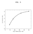
- FIG. 5 shows an example of the change in the composition of Zn of a ZnO thin film that is deposited using an atom layer deposition (ALD) by an example method that reduces the ratio of DEZ in the supplying process.
- ALD atom layer deposition
- the inflow ratio of Zn may be saturated gradually. In other words, as the number of Y sub-cycles is increased, the inflow ratio of Zn into the thin film may be reduced.
- the inflow ratio of Zn into the thin film may be controlled by controlling the number of Y sub-cycles. Also, because the layers are stacked in an atom layer unit, the inflow position of Zn(the position of charge trap site), may be controlled by controlling the number of Y sub-cycles.
- the horizontal and vertical distances between charge trap sites may be controlled arbitrarily. That is, the charge trap position and the density may be effectively controlled in the charge trap layer.
- FIG. 6 illustrates the programming/erasing characteristics of a charge trap semiconductor memory device manufactured according to example embodiments.
- the variation of a flat band voltage was recorded by varying the programming time from 10 -7 s to 1 s at a voltage applied to the gate electrode in the range of 14 V to 20 V.
- the variation of a flat band voltage was recorded by varying the erasing time from 10 -7 s to 1 s at a voltage applied to the gate electrode in the range of -20 V to -14 V.
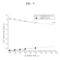
- FIG. 7 illustrates a retention characteristic of the sample indicating the programming/erasing characteristics of FIG. 6 .
- FIG. 7 shows the variation of the flat band voltage according to time when the charge trap semiconductor memory device (the sample) is programmed at a voltage of 20 V applied to the gate electrode 27 and a programming time of 0.1 s, and erased at a voltage of - 20 V and at an erasing time of 1 ms in room temperature.
- FIG. 7 shows that a sufficient memory window can be secured even after 10 years.
- the charge trap layer may be formed by SMI film containing a metal impurity whose position may be controlled.
- the trap position and the density in the charge trap layer may be effectively controlled. Accordingly, a non-volatile semiconductor memory device having improved retention characteristics may be realized.
Landscapes
- Semiconductor Memories (AREA)
- Non-Volatile Memory (AREA)
- Formation Of Insulating Films (AREA)
Applications Claiming Priority (1)
| Application Number | Priority Date | Filing Date | Title |
|---|---|---|---|
| KR1020060120142A KR101146589B1 (ko) | 2006-11-30 | 2006-11-30 | 전하 트랩형 반도체 메모리 소자 |
Publications (2)
| Publication Number | Publication Date |
|---|---|
| EP1928014A2 true EP1928014A2 (de) | 2008-06-04 |
| EP1928014A3 EP1928014A3 (de) | 2009-05-13 |
Family
ID=39184651
Family Applications (1)
| Application Number | Title | Priority Date | Filing Date |
|---|---|---|---|
| EP20070121684 Withdrawn EP1928014A3 (de) | 2006-11-30 | 2007-11-27 | Ladungsfallenschicht für eine Ladungsfallen-Halbleiterspeichervorrichtung und Herstellungsverfahren dafür |
Country Status (5)
| Country | Link |
|---|---|
| US (1) | US7795159B2 (de) |
| EP (1) | EP1928014A3 (de) |
| JP (1) | JP2008147655A (de) |
| KR (1) | KR101146589B1 (de) |
| CN (1) | CN101192532B (de) |
Families Citing this family (11)
| Publication number | Priority date | Publication date | Assignee | Title |
|---|---|---|---|---|
| KR20090025629A (ko) * | 2007-09-06 | 2009-03-11 | 삼성전자주식회사 | 비휘발성 메모리 소자 및 그 형성방법 |
| KR100975941B1 (ko) * | 2008-02-26 | 2010-08-13 | 경희대학교 산학협력단 | 금속도핑에 의해 형성된 불순물트랩을 전하저장준위로이용한 비휘발성 메모리소자 및 그 제조방법 |
| JP5703354B2 (ja) * | 2008-11-26 | 2015-04-15 | 株式会社日立国際電気 | 半導体装置の製造方法及び基板処理装置 |
| CN102074471B (zh) * | 2009-11-24 | 2012-09-05 | 上海华虹Nec电子有限公司 | Sonos闪存器件采用氧化铝作隧穿电介质膜的制作方法 |
| RU2483318C2 (ru) * | 2011-07-06 | 2013-05-27 | Открытое акционерное общество "Конструкторское бюро по радиоконтролю систем управления, навигации и связи" (ОАО "КБ "Связь") | Способ измерения времени прихода сигнала и устройство для его реализации |
| KR102533125B1 (ko) * | 2015-09-03 | 2023-05-15 | 캘리포니아 인스티튜트 오브 테크놀로지 | 높은-k 유전체를 특징화하는 시스템 및 방법 |
| TWI795596B (zh) * | 2015-10-05 | 2023-03-11 | 加州理工學院 | 特徵化高介電係數電介質之方法及其光學系統 |
| US11946863B2 (en) | 2018-05-15 | 2024-04-02 | Femtometrix, Inc. | Second Harmonic Generation (SHG) optical inspection system designs |
| JP7170273B2 (ja) * | 2019-06-06 | 2022-11-14 | 日本電信電話株式会社 | 強誘電体薄膜およびその製造方法ならびにデバイス |
| KR20240109477A (ko) * | 2023-01-04 | 2024-07-11 | 삼성전자주식회사 | 수직형 비휘발성 메모리 소자 및 이를 포함하는 전자 장치 |
| KR102935622B1 (ko) | 2024-08-19 | 2026-03-06 | 서울시립대학교 산학협력단 | 새로운 실리콘 반도체 제조 방법 및 그 제조 방법으로 제조된 실리콘 반도체 |
Family Cites Families (9)
| Publication number | Priority date | Publication date | Assignee | Title |
|---|---|---|---|---|
| US6548825B1 (en) * | 1999-06-04 | 2003-04-15 | Matsushita Electric Industrial Co., Ltd. | Semiconductor device including barrier layer having dispersed particles |
| KR100678626B1 (ko) * | 2004-01-29 | 2007-02-05 | 삼성전자주식회사 | 미세 전자 소자의 다층 유전체막 및 그 제조 방법 |
| US7221017B2 (en) * | 2002-07-08 | 2007-05-22 | Micron Technology, Inc. | Memory utilizing oxide-conductor nanolaminates |
| KR100885910B1 (ko) * | 2003-04-30 | 2009-02-26 | 삼성전자주식회사 | 게이트 적층물에 oha막을 구비하는 비 휘발성 반도체메모리 장치 및 그 제조방법 |
| CN1864253A (zh) * | 2003-10-06 | 2006-11-15 | 马萨诸塞州技术研究院 | 非易失性存储装置 |
| US6998317B2 (en) * | 2003-12-18 | 2006-02-14 | Sharp Laboratories Of America, Inc. | Method of making a non-volatile memory using a plasma oxidized high-k charge-trapping layer |
| US7256450B2 (en) * | 2004-03-24 | 2007-08-14 | Micron Technology, Inc. | NROM memory device with a high-permittivity gate dielectric formed by the low temperature oxidation of metals |
| US7365027B2 (en) * | 2005-03-29 | 2008-04-29 | Micron Technology, Inc. | ALD of amorphous lanthanide doped TiOx films |
| KR20060113081A (ko) * | 2005-04-29 | 2006-11-02 | 삼성전자주식회사 | 금속 불순물이 도핑된 실리콘 나노닷을 포함한 메모리 소자 |
-
2006
- 2006-11-30 KR KR1020060120142A patent/KR101146589B1/ko active Active
-
2007
- 2007-11-27 EP EP20070121684 patent/EP1928014A3/de not_active Withdrawn
- 2007-11-30 US US11/987,425 patent/US7795159B2/en active Active
- 2007-11-30 JP JP2007311247A patent/JP2008147655A/ja active Pending
- 2007-11-30 CN CN2007101963209A patent/CN101192532B/zh active Active
Also Published As
| Publication number | Publication date |
|---|---|
| US7795159B2 (en) | 2010-09-14 |
| JP2008147655A (ja) | 2008-06-26 |
| KR101146589B1 (ko) | 2012-05-16 |
| CN101192532B (zh) | 2011-07-06 |
| KR20080049500A (ko) | 2008-06-04 |
| CN101192532A (zh) | 2008-06-04 |
| US20080131710A1 (en) | 2008-06-05 |
| EP1928014A3 (de) | 2009-05-13 |
Similar Documents
| Publication | Publication Date | Title |
|---|---|---|
| US7795159B2 (en) | Charge trap layer for a charge trap semiconductor memory device and method of manufacturing the same | |
| KR100894098B1 (ko) | 빠른 소거속도 및 향상된 리텐션 특성을 갖는 불휘발성메모리소자 및 그 제조방법 | |
| US7419888B2 (en) | Method of forming a silicon-rich nanocrystalline structure by an atomic layer deposition process and method of manufacturing a non-volatile semiconductor device using the same | |
| US7646056B2 (en) | Gate structures of a non-volatile memory device and methods of manufacturing the same | |
| KR100615093B1 (ko) | 나노크리스탈을 갖는 비휘발성 메모리 소자의 제조방법 | |
| KR101281911B1 (ko) | Mos형 반도체 메모리 장치, nand형 메모리 셀 어레이, 및 nor형 메모리 셀 어레이 | |
| KR100890040B1 (ko) | 전하트랩층을 갖는 불휘발성 메모리소자 및 그 제조방법 | |
| US6642573B1 (en) | Use of high-K dielectric material in modified ONO structure for semiconductor devices | |
| KR100843229B1 (ko) | 하이브리드 구조의 전하 트랩막을 포함하는 플래쉬 메모리소자 및 그 제조 방법 | |
| US7948025B2 (en) | Non-volatile memory device having charge trapping layer and method for fabricating the same | |
| US7736975B2 (en) | Method for manufacturing non-volatile memory device having charge trap layer | |
| US8044454B2 (en) | Non-volatile memory device | |
| US7800162B2 (en) | Nonvolatile memory device and method of fabricating the same | |
| US7163860B1 (en) | Method of formation of gate stack spacer and charge storage materials having reduced hydrogen content in charge trapping dielectric flash memory device | |
| KR100819003B1 (ko) | 비휘발성 메모리 소자 제조 방법 | |
| KR20100123889A (ko) | Mos형 반도체 메모리 장치의 제조 방법 및 플라즈마 cvd 장치 | |
| KR100819002B1 (ko) | 비휘발성 메모리 소자 제조 방법 | |
| KR20090017040A (ko) | 비휘발성 메모리 소자 및 그 제조방법 | |
| KR100641074B1 (ko) | 전하 트랩 타입의 비휘발성 메모리 장치 및 그 제조 방법 | |
| KR100811272B1 (ko) | 전하트랩층을 갖는 불휘발성 메모리소자 및 그 제조방법 | |
| Eun | Charge Trapping Flash Memory With High-k Dielectrics |
Legal Events
| Date | Code | Title | Description |
|---|---|---|---|
| PUAI | Public reference made under article 153(3) epc to a published international application that has entered the european phase |
Free format text: ORIGINAL CODE: 0009012 |
|
| AK | Designated contracting states |
Kind code of ref document: A2 Designated state(s): AT BE BG CH CY CZ DE DK EE ES FI FR GB GR HU IE IS IT LI LT LU LV MC MT NL PL PT RO SE SI SK TR |
|
| AX | Request for extension of the european patent |
Extension state: AL BA HR MK RS |
|
| PUAL | Search report despatched |
Free format text: ORIGINAL CODE: 0009013 |
|
| AK | Designated contracting states |
Kind code of ref document: A3 Designated state(s): AT BE BG CH CY CZ DE DK EE ES FI FR GB GR HU IE IS IT LI LT LU LV MC MT NL PL PT RO SE SI SK TR |
|
| AX | Request for extension of the european patent |
Extension state: AL BA HR MK RS |
|
| RIC1 | Information provided on ipc code assigned before grant |
Ipc: H01L 29/788 20060101ALI20090404BHEP Ipc: H01L 29/423 20060101ALI20090404BHEP Ipc: H01L 29/792 20060101ALI20090404BHEP Ipc: H01L 21/28 20060101AFI20080326BHEP |
|
| AKX | Designation fees paid | ||
| REG | Reference to a national code |
Ref country code: DE Ref legal event code: 8566 |
|
| STAA | Information on the status of an ep patent application or granted ep patent |
Free format text: STATUS: THE APPLICATION IS DEEMED TO BE WITHDRAWN |
|
| 18D | Application deemed to be withdrawn |
Effective date: 20091114 |