EP1928041B1 - Procédé de fabrication d'un affichage électroluminescent organique - Google Patents
Procédé de fabrication d'un affichage électroluminescent organique Download PDFInfo
- Publication number
- EP1928041B1 EP1928041B1 EP07252153.7A EP07252153A EP1928041B1 EP 1928041 B1 EP1928041 B1 EP 1928041B1 EP 07252153 A EP07252153 A EP 07252153A EP 1928041 B1 EP1928041 B1 EP 1928041B1
- Authority
- EP
- European Patent Office
- Prior art keywords
- layer
- organic light
- light emitting
- fabricating
- substrate
- Prior art date
- Legal status (The legal status is an assumption and is not a legal conclusion. Google has not performed a legal analysis and makes no representation as to the accuracy of the status listed.)
- Not-in-force
Links
- 238000004519 manufacturing process Methods 0.000 title claims description 34
- 239000000758 substrate Substances 0.000 claims description 247
- 239000004065 semiconductor Substances 0.000 claims description 64
- 239000007767 bonding agent Substances 0.000 claims description 47
- 238000005538 encapsulation Methods 0.000 claims description 34
- 239000011521 glass Substances 0.000 claims description 16
- 239000008393 encapsulating agent Substances 0.000 claims description 14
- 229910052751 metal Inorganic materials 0.000 claims description 11
- 239000002184 metal Substances 0.000 claims description 11
- 229920003023 plastic Polymers 0.000 claims description 8
- 229920000642 polymer Polymers 0.000 claims description 8
- 239000003223 protective agent Substances 0.000 claims description 8
- QDOXWKRWXJOMAK-UHFFFAOYSA-N dichromium trioxide Chemical compound O=[Cr]O[Cr]=O QDOXWKRWXJOMAK-UHFFFAOYSA-N 0.000 claims description 6
- 239000004033 plastic Substances 0.000 claims description 6
- 239000000853 adhesive Substances 0.000 claims description 5
- 230000001070 adhesive effect Effects 0.000 claims description 5
- 229920006332 epoxy adhesive Polymers 0.000 claims description 5
- 229910052782 aluminium Inorganic materials 0.000 claims description 4
- 239000011368 organic material Substances 0.000 claims description 4
- 229910001316 Ag alloy Inorganic materials 0.000 claims description 3
- 239000011248 coating agent Substances 0.000 claims description 3
- 238000000576 coating method Methods 0.000 claims description 3
- 229910052737 gold Inorganic materials 0.000 claims description 3
- 229910010272 inorganic material Inorganic materials 0.000 claims description 3
- 239000011147 inorganic material Substances 0.000 claims description 3
- CPLXHLVBOLITMK-UHFFFAOYSA-N magnesium oxide Inorganic materials [Mg]=O CPLXHLVBOLITMK-UHFFFAOYSA-N 0.000 claims description 3
- 229910052709 silver Inorganic materials 0.000 claims description 3
- 229910000831 Steel Inorganic materials 0.000 claims description 2
- 239000010959 steel Substances 0.000 claims description 2
- 239000010410 layer Substances 0.000 description 322
- 238000000034 method Methods 0.000 description 76
- 239000000463 material Substances 0.000 description 30
- 238000010521 absorption reaction Methods 0.000 description 17
- 239000010408 film Substances 0.000 description 15
- 239000010409 thin film Substances 0.000 description 15
- 239000011229 interlayer Substances 0.000 description 10
- 238000002425 crystallisation Methods 0.000 description 9
- 229910045601 alloy Inorganic materials 0.000 description 8
- 239000000956 alloy Substances 0.000 description 8
- 239000011241 protective layer Substances 0.000 description 7
- 238000005530 etching Methods 0.000 description 6
- 238000010438 heat treatment Methods 0.000 description 6
- 238000005516 engineering process Methods 0.000 description 5
- 238000000926 separation method Methods 0.000 description 5
- 230000004888 barrier function Effects 0.000 description 4
- 238000004140 cleaning Methods 0.000 description 4
- 230000008025 crystallization Effects 0.000 description 4
- 230000008030 elimination Effects 0.000 description 4
- 238000003379 elimination reaction Methods 0.000 description 4
- 238000011049 filling Methods 0.000 description 4
- 238000002347 injection Methods 0.000 description 4
- 239000007924 injection Substances 0.000 description 4
- 229910044991 metal oxide Inorganic materials 0.000 description 4
- 229910021420 polycrystalline silicon Inorganic materials 0.000 description 4
- 239000000126 substance Substances 0.000 description 4
- 229910020091 MgCa Inorganic materials 0.000 description 3
- 101100003996 Mus musculus Atrn gene Proteins 0.000 description 3
- VYPSYNLAJGMNEJ-UHFFFAOYSA-N Silicium dioxide Chemical compound O=[Si]=O VYPSYNLAJGMNEJ-UHFFFAOYSA-N 0.000 description 3
- 230000001413 cellular effect Effects 0.000 description 3
- 230000000694 effects Effects 0.000 description 3
- 230000005525 hole transport Effects 0.000 description 3
- 239000007788 liquid Substances 0.000 description 3
- 239000011159 matrix material Substances 0.000 description 3
- 229910052581 Si3N4 Inorganic materials 0.000 description 2
- QAOWNCQODCNURD-UHFFFAOYSA-L Sulfate Chemical compound [O-]S([O-])(=O)=O QAOWNCQODCNURD-UHFFFAOYSA-L 0.000 description 2
- 229910000828 alnico Inorganic materials 0.000 description 2
- UMIVXZPTRXBADB-UHFFFAOYSA-N benzocyclobutene Chemical compound C1=CC=C2CCC2=C1 UMIVXZPTRXBADB-UHFFFAOYSA-N 0.000 description 2
- 230000000903 blocking effect Effects 0.000 description 2
- 239000003795 chemical substances by application Substances 0.000 description 2
- 238000000151 deposition Methods 0.000 description 2
- 230000005484 gravity Effects 0.000 description 2
- 238000000227 grinding Methods 0.000 description 2
- 150000004820 halides Chemical class 0.000 description 2
- 230000000149 penetrating effect Effects 0.000 description 2
- VLTRZXGMWDSKGL-UHFFFAOYSA-M perchlorate Inorganic materials [O-]Cl(=O)(=O)=O VLTRZXGMWDSKGL-UHFFFAOYSA-M 0.000 description 2
- VLTRZXGMWDSKGL-UHFFFAOYSA-N perchloric acid Chemical compound OCl(=O)(=O)=O VLTRZXGMWDSKGL-UHFFFAOYSA-N 0.000 description 2
- 230000005855 radiation Effects 0.000 description 2
- 229910052761 rare earth metal Inorganic materials 0.000 description 2
- 150000002910 rare earth metals Chemical class 0.000 description 2
- 239000000243 solution Substances 0.000 description 2
- 229910000859 α-Fe Inorganic materials 0.000 description 2
- -1 AINd Inorganic materials 0.000 description 1
- 229910000881 Cu alloy Inorganic materials 0.000 description 1
- 229910001182 Mo alloy Inorganic materials 0.000 description 1
- 229910016048 MoW Inorganic materials 0.000 description 1
- 239000004642 Polyimide Substances 0.000 description 1
- XUIMIQQOPSSXEZ-UHFFFAOYSA-N Silicon Chemical compound [Si] XUIMIQQOPSSXEZ-UHFFFAOYSA-N 0.000 description 1
- NIXOWILDQLNWCW-UHFFFAOYSA-N acrylic acid group Chemical group C(C=C)(=O)O NIXOWILDQLNWCW-UHFFFAOYSA-N 0.000 description 1
- 238000004026 adhesive bonding Methods 0.000 description 1
- 229910021417 amorphous silicon Inorganic materials 0.000 description 1
- 238000005452 bending Methods 0.000 description 1
- 229910052804 chromium Inorganic materials 0.000 description 1
- 229910052681 coesite Inorganic materials 0.000 description 1
- 229910052802 copper Inorganic materials 0.000 description 1
- 229910052906 cristobalite Inorganic materials 0.000 description 1
- 230000002950 deficient Effects 0.000 description 1
- 229910003460 diamond Inorganic materials 0.000 description 1
- 239000010432 diamond Substances 0.000 description 1
- 230000009977 dual effect Effects 0.000 description 1
- 230000005684 electric field Effects 0.000 description 1
- NJWNEWQMQCGRDO-UHFFFAOYSA-N indium zinc Chemical compound [Zn].[In] NJWNEWQMQCGRDO-UHFFFAOYSA-N 0.000 description 1
- AMGQUBHHOARCQH-UHFFFAOYSA-N indium;oxotin Chemical compound [In].[Sn]=O AMGQUBHHOARCQH-UHFFFAOYSA-N 0.000 description 1
- 238000005224 laser annealing Methods 0.000 description 1
- 239000000155 melt Substances 0.000 description 1
- 239000007769 metal material Substances 0.000 description 1
- 150000002894 organic compounds Chemical class 0.000 description 1
- 229920001721 polyimide Polymers 0.000 description 1
- 229920005591 polysilicon Polymers 0.000 description 1
- 230000003014 reinforcing effect Effects 0.000 description 1
- 238000007789 sealing Methods 0.000 description 1
- 239000003566 sealing material Substances 0.000 description 1
- 238000004904 shortening Methods 0.000 description 1
- 229910052710 silicon Inorganic materials 0.000 description 1
- 239000010703 silicon Substances 0.000 description 1
- 239000000377 silicon dioxide Substances 0.000 description 1
- HQVNEWCFYHHQES-UHFFFAOYSA-N silicon nitride Chemical compound N12[Si]34N5[Si]62N3[Si]51N64 HQVNEWCFYHHQES-UHFFFAOYSA-N 0.000 description 1
- 229910052814 silicon oxide Inorganic materials 0.000 description 1
- 239000007790 solid phase Substances 0.000 description 1
- 238000007711 solidification Methods 0.000 description 1
- 230000008023 solidification Effects 0.000 description 1
- 230000002269 spontaneous effect Effects 0.000 description 1
- 229910052682 stishovite Inorganic materials 0.000 description 1
- 229910052719 titanium Inorganic materials 0.000 description 1
- 229910052905 tridymite Inorganic materials 0.000 description 1
- XLOMVQKBTHCTTD-UHFFFAOYSA-N zinc oxide Inorganic materials [Zn]=O XLOMVQKBTHCTTD-UHFFFAOYSA-N 0.000 description 1
- 239000011787 zinc oxide Substances 0.000 description 1
Images




Classifications
-
- H—ELECTRICITY
- H05—ELECTRIC TECHNIQUES NOT OTHERWISE PROVIDED FOR
- H05B—ELECTRIC HEATING; ELECTRIC LIGHT SOURCES NOT OTHERWISE PROVIDED FOR; CIRCUIT ARRANGEMENTS FOR ELECTRIC LIGHT SOURCES, IN GENERAL
- H05B33/00—Electroluminescent light sources
- H05B33/02—Details
- H05B33/04—Sealing arrangements, e.g. against humidity
-
- H—ELECTRICITY
- H10—SEMICONDUCTOR DEVICES; ELECTRIC SOLID-STATE DEVICES NOT OTHERWISE PROVIDED FOR
- H10K—ORGANIC ELECTRIC SOLID-STATE DEVICES
- H10K59/00—Integrated devices, or assemblies of multiple devices, comprising at least one organic light-emitting element covered by group H10K50/00
- H10K59/80—Constructional details
- H10K59/87—Passivation; Containers; Encapsulations
- H10K59/871—Self-supporting sealing arrangements
- H10K59/8722—Peripheral sealing arrangements, e.g. adhesives, sealants
-
- H—ELECTRICITY
- H05—ELECTRIC TECHNIQUES NOT OTHERWISE PROVIDED FOR
- H05B—ELECTRIC HEATING; ELECTRIC LIGHT SOURCES NOT OTHERWISE PROVIDED FOR; CIRCUIT ARRANGEMENTS FOR ELECTRIC LIGHT SOURCES, IN GENERAL
- H05B33/00—Electroluminescent light sources
- H05B33/02—Details
-
- H—ELECTRICITY
- H05—ELECTRIC TECHNIQUES NOT OTHERWISE PROVIDED FOR
- H05B—ELECTRIC HEATING; ELECTRIC LIGHT SOURCES NOT OTHERWISE PROVIDED FOR; CIRCUIT ARRANGEMENTS FOR ELECTRIC LIGHT SOURCES, IN GENERAL
- H05B33/00—Electroluminescent light sources
- H05B33/10—Apparatus or processes specially adapted to the manufacture of electroluminescent light sources
-
- H—ELECTRICITY
- H10—SEMICONDUCTOR DEVICES; ELECTRIC SOLID-STATE DEVICES NOT OTHERWISE PROVIDED FOR
- H10K—ORGANIC ELECTRIC SOLID-STATE DEVICES
- H10K50/00—Organic light-emitting devices
- H10K50/80—Constructional details
- H10K50/84—Passivation; Containers; Encapsulations
- H10K50/842—Containers
- H10K50/8426—Peripheral sealing arrangements, e.g. adhesives, sealants
-
- H—ELECTRICITY
- H10—SEMICONDUCTOR DEVICES; ELECTRIC SOLID-STATE DEVICES NOT OTHERWISE PROVIDED FOR
- H10K—ORGANIC ELECTRIC SOLID-STATE DEVICES
- H10K2102/00—Constructional details relating to the organic devices covered by this subclass
- H10K2102/301—Details of OLEDs
- H10K2102/311—Flexible OLED
-
- H—ELECTRICITY
- H10—SEMICONDUCTOR DEVICES; ELECTRIC SOLID-STATE DEVICES NOT OTHERWISE PROVIDED FOR
- H10K—ORGANIC ELECTRIC SOLID-STATE DEVICES
- H10K71/00—Manufacture or treatment specially adapted for the organic devices covered by this subclass
-
- H—ELECTRICITY
- H10—SEMICONDUCTOR DEVICES; ELECTRIC SOLID-STATE DEVICES NOT OTHERWISE PROVIDED FOR
- H10K—ORGANIC ELECTRIC SOLID-STATE DEVICES
- H10K71/00—Manufacture or treatment specially adapted for the organic devices covered by this subclass
- H10K71/40—Thermal treatment, e.g. annealing in the presence of a solvent vapour
-
- H—ELECTRICITY
- H10—SEMICONDUCTOR DEVICES; ELECTRIC SOLID-STATE DEVICES NOT OTHERWISE PROVIDED FOR
- H10K—ORGANIC ELECTRIC SOLID-STATE DEVICES
- H10K77/00—Constructional details of devices covered by this subclass and not covered by groups H10K10/80, H10K30/80, H10K50/80 or H10K59/80
- H10K77/10—Substrates, e.g. flexible substrates
- H10K77/111—Flexible substrates
Definitions
- the present invention relates to a fabricating method of an organic light-emitting display, and more particularly, the present invention relates to a fabricating method capable of fabricating a thin organic light emitting display, shortening fabricating process time and preventing a substrate from being bent or damaged during the fabricating process.
- an organic light emitting display self-emits light by causing an electric current to flow through a fluorescent or phosphorescent organic compound and allowing an electron and a hole to be coupled to each other.
- an organic light emitting display can display an image by driving organic light emitting diodes, for example, n by m organic light emitting diodes, by a voltage or a current.
- organic light emitting diodes have a basic structure including an anode (ITO), an organic thin layer and a cathode electrode (metal).
- the organic thin layer is composed of an EMitting Layer (EML) which emits light when the electrons and the holes meet and thereby form an exciton, an Electron Transport Layer (ETL) for controlling the moving speed of the electrons, and a Hole Transport Layer (HTL) for controlling the moving speed of the holes.
- ETL Electron Transport Layer
- HTL Hole Transport Layer
- An Electron Injecting Layer (EIL) is further formed in the ETL for improving the effectiveness of the injection of electrons
- a Hole Injecting Layer (HIL) is further formed in the Hole Transport Layer for improving the effectiveness of the injection of holes.
- the organic light emitting display is by no means inferior to other devices because of a wide range of vision, a super high-speed response, and spontaneous light emitting, and it is possible to fabricate a thin light-weight device since the power consumption is low and a backlight is not required. Since it is fabricated at a low temperature and the fabricating processes are simple, the device is fabricated at a low cost. As organic thin layer material technology and the process technology are being developed rapidly, they are considered to be the technology that can replace the conventional flat display device.
- organic light emitting display since electronic devices, such as cellular telephones, Personal Digital Assistants (PDAs), notebook computers, computer monitors, televisions and so forth, have becomes slimmer, it is necessary for the organic light emitting display to have a thickness below about 1mm.
- PDAs Personal Digital Assistants
- the organic light emitting display since a protective layer technology that can substitute for an encapsulation technology has not been sufficiently developed, it is difficult to fabricate an organic light emitting display having a thickness below 1mm.
- Japanese Laid-Open Patent Publications Nos. 2005-340182 , 2005-222930 and 2005-222789 relate to a method of fabricating a thin organic light emitting display in which element layers (a semiconductor layer and an organic light emitting diode, etc.) are respectively formed on two glass substrates, and the glass substrates are then bonded to each other so that the respective element layers face each other and then the surfaces on which the element layers are not formed are removed by an etching or grinding process.
- element layers a semiconductor layer and an organic light emitting diode, etc.
- the above-noted fabricating method has a problem in that the fabricating process time greatly increases because after the semiconductor layer or the organic light emitting diode is formed on the respective glass substrates, the glass substrates are bonded to each other and are etched or ground. Moreover, such a conventional fabricating method has a problem in that the yield of production is low and the fabricating cost is expensive because the partly finished glass substrates are bonded to each other and the glass substrate, the semiconductor layer and the organic light emitting diode is damaged during bonding process.
- a fabricating method is conceivable in which after providing a glass substrate having a thickness below 1mm, an element layer is formed on the surface of the glass substrate.
- a fabricating method has a problem in that the glass substrate bends or contacts a moving device and is damaged during the moving process because the glass substrate is very thin.
- US2005/0285522 discloses an electro-luminescent display device that includes a substrate having a display region.
- a sealing substrate is provided that seals the display region in combination with the substrate via a sealing material.
- US2003/0020124 discloses a substrate support rim used in fabrication of organic light emitting diodes.
- the support rim is located at the edge of a substrate so as to reinforce the substrate.
- US5,811,866 discloses an active-matrix board that has a first light shield film disposed on a face side of a thin-film transistor, and a second light shield disposed on a reverse side of the transparent insulating substrate.
- JP2003173872 discloses an alignment device comprising a substrate holder that holds a flexible substrate with a magnetic film formed thereon. An electromagnet is provided to fix the flexible substrate with the magnetic film stuck thereon to the substrate holder.
- the present invention is conceived to solve the aforementioned problems, and it is an object of the present invention to provide a method of fabricating a thin organic light emitting display.
- Another object of the present invention is to shorten the fabricating process time by bonding two substrates.
- Another object of the present invention is to generate no defective exposure by preventing UV-rays from impinging upon an undesired portion of the substrate.
- Another object of the present invention to prevent a substrate from being bent or damaged during the fabricating process.
- a method of fabricating an organic light emitting display is provided as set out in Claim 1.
- Optional features of this aspect are set out in Claims 2 to 20.
- the organic light emitting display manufactured by the method according to the present invention can be easily applied to electronic devices, such as cellular telephones, Personal Digital Assistants (PDAs), notebook computers, computer monitors and televisions, by being made in a thin and compact size.
- electronic devices such as cellular telephones, Personal Digital Assistants (PDAs), notebook computers, computer monitors and televisions, by being made in a thin and compact size.
- PDAs Personal Digital Assistants
- notebook computers notebook computers
- computer monitors and televisions by being made in a thin and compact size.
- the organic light emitting display manufactured by the method according to the present invention prevents UV-rays from influencing the semiconductor layer or the organic light emitting diode through the substrate by forming the non-transmissive layer on the substrate.
- the organic light emitting display manufactured by the method according to the present invention prevents the substrate from being damaged due to external forces as rigidity is increased by forming the bonding agent on one side of the under surface of the substrate.
- the method of fabricating the organic light emitting display according to the present invention can shorten the overall process time by about 50% as the semiconductor process and the organic thin layer process (including cleaning, etching, exposure, development and heat treatment) are executed simultaneously by bonding two substrates having a thickness of 0.05 to 1mm, and preventing the substrate from being bent by means of obtaining a specific rigidity.
- the fabricating method according to the present invention prevents UV-rays due to the exposure process from influencing the other substrate on the opposite side during the fabricating process by forming the non-transmissive layer on the under surface of the substrate.
- the fabricating method according to the present invention prevents the organic light emitting display from being bent or damaged due to the repulsion force between the magnetic layer and the transporting machine transporting the magnetic layer (since another magnetic layer repulsive to the magnetic layer is formed on the transporting machine) or the force of gravity during fabricating process as rigidity is increased by forming the non-transmissive layer/magnetic layer on the under surface of the substrate.
- the fabricating method according to the present invention prevents the substrates from contacting each other, and thus, from being damaged by forming the non-transmissive layer/magnetic layer/anti-friction layer or the non-transmissive layer/anti-friction layer on the under surface of the substrate.
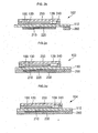
- FIGs. 2a-2d a cross-sectional views of organic light emitting displays are illustrated.
- an organic light emitting display 101 includes a substrate 110, a semiconductor layer 130 formed on the substrate 110, a driver circuit 139 formed on one side of the semiconductor layer 130, an organic light emitting diode 190 formed on the semiconductor layer 130, a encapsulant 240 formed on a top surface periphery of the substrate 110, which is an outer periphery of the semiconductor layer 130, the organic light emitting diode 190 and the driver circuit 139, an encapsulation substrate 250 bonded to the encapsulant 240, and a bonding agent 260 formed on a under surface of the substrate 110 which is opposite to the encapsulant 240.
- the bonding agent can be at least one of an epoxy adhesive, an UV-ray setting adhesive, a frit or an equivalent thereof.
- the material is not restricted thereto.
- a frit is used as the encapsulant 240, an encapsulating operation can be executed by using a laser beam because the frit must be heated to a predetermined temperature. After arranging the frit between the substrate 110 and the encapsulation substrate 250, if the laser beam irradiates the frit, then the frit melts and the substrate 110 and the encapsulation substrate 250 are strongly attached to each other.
- the encapsulation substrate 250 can be formed of a transparent glass, a transparent plastic, a transparent polymer or an equivalent thereof. However, the material is not restricted thereto.
- the bonding agent 260 is formed during a fabricating process of the organic light emitting display according to an embodiment of the present invention, and reinforces the strength of the-substrate.
- the bonding agent 260 can be formed in the vicinity of at least on one side of the under surface of the substrate 110.
- the bonding agent 260 can be formed in the vicinity of every edge of the under surface of the substrate 110.
- the bonding agent 260 can be formed on the under surface of the substrate 110 corresponding to the outer periphery of the semiconductor layer 130 and the organic light emitting diode 190.
- the bonding agent 260 can be formed on the under surface of the substrate 110 corresponding to the outer periphery of the encapsulant 240 and the encapsulation substrate 250.
- the bonding agent 260 can be formed of at least one of an epoxy adhesive, a UV-ray setting adhesive or an equivalent thereof. However, the material of the bonding agent 260 is not restricted thereto.
- the bonding agent 260 can be formed to have a thickness of about 10 to 100 ⁇ m. If the thickness of the bonding agent is 10 ⁇ m or below, the rigidity is weak when two substrates contact each other during the fabricating process, and if the thickness of the bonding agent is 100 ⁇ m or above, the bonded substrates are too thick. As described above, in order to arrange the bonding agent 260 on the outer periphery of the semiconductor layer 130, the organic light emitting diode 190, the encapsulant 240 and the encapsulation substrate 250, the substrate 110 must have a larger region than that of the encapsulation substrate 250. A non-transmissive layer 210 can be further formed on the under surface of the substrate 110 to prevent UV-rays from penetrating into the semiconductor layer 130 or the organic light emitting diode 190.
- a non-transmissive layer 210 and a magnetic layer 220 can be formed on the under surface of the substrate 110 in sequence.
- a non-transmissive layer 210, a magnetic layer 220 and an anti-friction layer 230 can be formed on the under surface of the substrate 110 in sequence.
- a non-trransmissive layer 210 and an anti-friction layer 230 can be formed on the under surface of the substrate 110 in sequence.
- the non-transmissive layer 210, the magnetic layer 220 and the anti-friction layer 230 are described in more detail below.
- a transparent moisture absorption layer which is not illustrated in the drawings can be formed on the under surface of the encapsulation substrate 250. That is, the transparent moisture absorption layer which is able to absorb moisture without blocking light can be formed on the under surface of the encapsulation substrate 250, since the organic light emitting diode 190 is vulnerable to moisture. This transparent moisture absorption layer is more advantageous as it is getting thicker as long as the transparency is obtained. Typically, it is preferable that the thickness of transparent moisture absorption layer is in a range of 0.1 to 300 ⁇ m.
- the transparent moisture absorption layer can be made of alkaline metallic oxide, alkaline earth metallic oxide, metallic halide, metallic sulfate, metallic perchlorate, P 2 O 5 or an equivalent thereof having an average grain size of 100nm or below, in particular 20 to 100nm.
- the material is not restricted thereto.
- moisture can be absorbed by filling up the space between the substrate 110 and the encapsulation substrate 250 with at least one of layered inorganic substance, polymer, hardening agent or an equivalent thereof, instead of forming the transparent moisture absorption layer on the encapsulation substrate 250. After this filling, a heat treatment process is performed, so that these materials are hardened.
- a light reflection effect due to external light can be prevented by arranging a polarizer film to the surface of the encapsulation substrate 250.
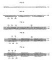
- Figs. 3a to 3d are cross-sectional views of organic light emitting displays before the encapsulation substrate is encapsulated.
- the organic light emitting display 101 includes a substrate 110, a buffer layer 120 formed on the substrate 110, a semiconductor layer 130 formed on the buffer layer 120, a gate insulating layer 140 formed on the semiconductor layer 130, a gate electrode 150 formed on the gate insulating layer 140, an inter-layer dielectric layer 160 formed on the gate electrode 150, a source/drain electrode 170 formed on the inter-layer dielectric layer 160, an insulating layer 180 formed on the source/drain electrode 170, an organic light emitting diode 190 formed on the insulating layer 180, and a pixel defining film 200 formed on the insulating layer 180 which is disposed at an outer periphery of the organic light emitting diode 190.
- the top surface and the under surface of the substrate 110 are parallel to each other, and a thickness between the top and under surfaces can be formed to be 0.05 to 1mm. If the thickness of the substrate 110 is 0.05mm or below, the substrate is easily damaged by cleaning, etching or heat treatment processes, and is vulnerable to external forces. If the thickness the substrate 110 is 1 mm or above, it is impossible to apply the substrate to various thin display devices.
- the substrate 110 can be formed of a material selected from a typical glass, plastic, polymer or an equivalent thereof. However, the present invention is not restricted to these materials.
- the buffer layer 120 is formed on the top surface of the substrate 110. This buffer layer 120 prevents H 2 O, H 2 or H 2 , etc from infiltrating into the semiconductor layer 130 or the organic light emitting diode 190 through the substrate 110.
- the buffer layer 120 can be made of at least one material selected from SiO 2 , Si 3 N 4 , or equivalents thereof which are easily made during the semiconductor process. However, the present invention is not restricted thereto. This buffer layer 120 can be omitted, if necessary.
- the semiconductor layer 130 is formed on the top surface of the buffer layer 120.
- This semiconductor layer 130 includes source/drain regions 132 formed on two sides opposite to each other, and a channel region 134 formed between the source/drain regions 132.
- the semiconductor layer 130 can be a thin film transistor.
- This thin film transistor can be at least one of an amorphous Si thin film transistor, poly Si thin film transistor, organic thin layer transistor, micro Si thin film transistor or the equivalent thereof.
- the present invention is not restricted to these thin film transistors.
- the poly Si thin film transistor can be made according to at least one method including a crystallization method using a laser at low temperature, a crystallization method using a metal, a crystallization method using high pressure, or the equivalent thereof.
- a crystallization method using a laser can be Excimer Laser Annealing (ELA), Sequential Lateral Solidification (SLS), Thin Beam Direction Crystallization (TDX) and so on.
- ELA Excimer Laser Annealing
- SLS Sequential Lateral Solidification
- TDX Thin Beam Direction Crystallization
- the present invention is not restricted to these methods.
- the crystallization method using a metal can be Solid Phases Crystallization (SPC), Metal Induced Crystallization (MIC), Metal Induced Lateral Crystallization (MILC), Super Grained Silicon (SGS) and so on.
- SPC Solid Phases Crystallization
- MIC Metal Induced Crystallization
- MILC Metal Induced Lateral Crystallization
- SGS Super Grained Silicon
- the thin film resistor can be one of PMOS, NMOS or the equivalent thereof.
- the present invention is not restricted thereto.
- the gate insulating layer 140 is formed on the top surface of the semiconductor layer 130. This gate insulating layer 140 is formed on the buffer layer 120 on the outer periphery of the semiconductor layer 130 and on the semiconductor layer 130 itself but with a gap provided over each of the two source/drain regions 132.
- the gate insulating layer 140 can be made of at least one of a silicon oxide film, a silicon nitride film, an inorganic film or an equivalent thereof which are easily obtained during the semiconductor process. However, the material is not restricted thereto.
- the gate electrode 150 is formed on the top surface of the gate insulating layer 140 that is provided on the semiconductor layer 130. More specifically, the gate electrode 150 is formed on the gate insulating layer 140 corresponding to the channel region 134 of the semiconductor layer 130. As known to those skilled in the art, this gate electrode 150 makes a hole or a channel of an electron in the channel region 134 by applying an electric field to the channel region 134 of the gate insulating layer 140.
- the gate electrode can be made of a typical metal (MoW, Ti, Cu, Al, AINd, Cr, Mo alloy, Cu alloy, A1 alloy, etc.), a doped poly silicon or the equivalent thereof. However, the material is not restricted thereto.
- the inter-layer dielectric layer 160 is formed on the top surface of the gate electrode 150 and on the top surface of the gate insulating layer 140 on the outer periphery of the gate electrode 150.
- the inter-layer dielectric layer 160 can be formed of any one of polymers, plastics, glasses or the equivalent thereof. However, the material of the inter-layer dielectric layer 160 is not restricted thereto.
- Two source/drain electrodes 170 are formed on the top surface of the inter-layer dielectric layer 160. Each has an electrically conductive contact 176, which penetrates through the inter-layer dielectric layer 160, and which connects the source/drain electrode 170 and the semiconductor layer 130. That is, the source/drain regions 132 of the semiconductor layer 130 and the source/drain electrodes 170 are electrically coupled by the electrically conductive contacts 176.
- the source/drain electrodes 170 can be formed of the same metal material as the gate electrode 150. However, the material is not restricted thereto.
- the above-described semiconductor layer 130 (the thin film transistor) is defined as a coplanar structure.
- the semiconductor layer 130 described in the present invention is not restricted to the coplanar structure, and can be any structure known hereto, for example, the structure can be at least one of an inverted coplanar structure, a staggered structure, an inverted staggered structure or an equivalent thereof.
- the semiconductor layer 130 of the present invention is not restricted thereto.
- the insulating layer 180 is formed on the top surface of the source/drain electrodes 170 and the surrounding portions of the inter-layer dielectric layer 160.
- the insulating layer 180 includes a protective layer 182 and an planarization layer 184.
- the protective layer 182 covers the source/drain electrodes 170 and the inter-layer dielectric layer 160, and protects the source/drain electrodes 170, the gate electrode 150 and so on.
- the protective layer 182 can be formed of a typical inorganic film or an equivalent thereof. However, the material of the protective layer 182 is not restricted thereto.
- the planarization layer 184 covers the protective layer 182.
- the planarization layer 184 makes the entire surface of the element flat, and can be formed of at least one of a Benzo Cyclo Butene (BCB), an acrylic or an equivalent thereof. However, the material is not restricted thereto.
- BCB Benzo Cyclo Butene
- the organic light emitting diode 190 is formed only on the top surface of the insulating layer 180.
- the organic light emitting diode 190 includes an anode 192, an organic light emitting thin film 194 formed on the top surface of the anode 192, and a cathode 196 formed on the top surface of the organic light emitting thin film 194.
- the anode 192 can be formed of Indium Tin Oxide (ITO)/Ag, ITO/Ag/ITO, ITO/Ag/ Indium Zinc Oxide(IZO) or the equivalent thereof.
- ITO Indium Tin Oxide
- ITO Indium Tin Oxide
- ITO Indium Tin Oxide
- ITO Indium Tin Oxide
- ITO Indium Tin Oxide
- ITO Indium Tin Oxide
- ITO Indium Tin Oxide
- ITO Indium Tin Oxide
- ITO Indium Tin Oxide
- ITO Indium Tin Oxide
- ITO/Ag/ITO ITO/Ag/ Indium
- the ITO is a transparent conductive layer in which a work function is uniform and a hole injecting barrier to the organic light emitting thin layer 194 is small
- the Ag is a layer that reflects the light emitted from the organic light emitting thin layer 194 to the top surface in a top emission system.
- the organic light emitting thin film 194 can include an EMitting Layer (EML) which emits as an exciton is formed by contact between electrons and holes, an electron transport layer (ETL) which controls the speed of electrons, and a Hole Transport Layer (HTL) which controls the speed of holes.
- ETL EMitting Layer
- ETL electron transport layer
- HTL Hole Transport Layer
- the cathode 196 can be at least one of Al, MgAg alloy, MgCa alloy or the equivalent thereof.
- the material of the cathode 196 of the present invention is not restricted thereto. If a top emission system is employed in the present invention, then the Al should be very thin. However, in this case, the resistance becomes high, and thus the electron injecting barrier becomes large.
- the MgAg alloy has an electron injecting barrier that is smaller than that of the Al, and the MgCa alloy has an electron injecting barrier that is smaller than that of the MgAg Alloy.
- the MgAg alloy and the MgCa alloy must be completely protected from the outside because they are sensitive to the surrounding environment and can oxidize and form an insulating layer.
- the anode 192 of the organic light emitting diode 190 and the source/drain electrodes 170 are electrically interconnected by an electrical contact 198 penetrating through the insulating layer 180 (the protective layer 182 and the planarization layer 184).
- the present invention has been described based on a top emission system in which the light is emitted in the direction outwardly from the upper part of the substrate 110, the present invention can be applied to a bottom emission system in which the light is emitted in the direction outwardly from the lower part of the substrate 110 or a dual emission system in which the light is simultaneously emitted in the directions from the upper and lower parts of the substrate 110.
- the pixel defining film 200 at an outer periphery of the organic light emitting diode 190, is formed on the top surface of the insulating layer 180.
- the pixel defining film 200 makes the boundary between a red organic light emitting diode, a green organic light emitting diode and a blue organic light emitting diode clear, and thus it makes the emitting boundary region between the pixels clear.
- the pixel defining film 200 can be formed of a polyimide or the equivalent thereof. However, the material of the pixel defining film 200 is not restricted thereto.
- a non-transmissive layer 210 is further formed on the under surface of the substrate 110.
- the non-transmissive layer 210 prevents UV-rays from impinging upon another substrate opposite to the UV-rays during the fabricating process which forms the semiconductor layer 130 and the organic light emitting diode 190 by bonding two substrates 110.
- the non-transmissive layer 210 prevents external UV-rays from impinging upon the semiconductor layer 130 and the organic light emitting diode 190 after the substrates 110 are divided into pieces.
- the non-transmissive layer 210 can be formed of a UV-ray protective agent or an equivalent thereof.
- the non-transmissive layer 210 can be formed of at least one of a metal through which UV-rays are blocked, a transparent UV-ray protective agent or an opaque UV-ray protective agent. If the non-transmissive layer 210 is a metal, then the non-transmissive layer can be formed of at least one of Cr, Cr 2 O 3 , Al, Au, Ag, MgO, a silver alloy or the equivalent thereof. However, the material is not restricted thereto. It is preferable that the non-transmissive layer 210 is formed to have a thickness of 500 to 3000 ⁇ .
- the thickness of the non-transmissive layer 210 is 500 ⁇ or below, then the elimination rate of UV-rays is low, and thus the semiconductor layer 130 or the organic light emitting diode 190 is affected by the radiation during or after the fabricating process. If the thickness of the non-transmissive layer 210 is 3000 ⁇ or above, then the elimination rate of UV-rays is good enough, but the non-transmissive layer 210 is too thick.
- a magnetic layer 220 can be further formed on the under surface of the non-transmissive layer 210.
- the magnetic layer 220 prevents the substrate 110 from being bent during the process forming of the semiconductor layer 130 and the organic light emitting diode 190 by bonding the two substrates 110. It is possible to prevent the substrate 110 from being bent by disposing a magnet with opposite polarity which repels the magnetic layer 220.
- the magnetic layer 220 can be formed of at least one of AlNiCo magnet, ferrite magnet, rare earth magnet, rubber magnet, plastic magnet or the equivalent thereof. However, the material of the magnetic layer 220 is not restricted thereto.
- the magnetic layer 220 it is possible to replace the magnetic layer by forming a pattern of an electromagnet instead of the permanent magnet or mounting an electromagnet. It is preferable that the magnetic layer 220 has a thickness of 10 to 100 ⁇ m. If the magnetic layer 220 is 10 ⁇ m or below, then it is hard to get sufficient magnetic force, and if the magnetic layer 220 is 100 ⁇ m or above, the magnetic layer is too thick.
- an anti-friction layer 230 can be further formed on the under surface of the magnetic layer 220.
- the anti-friction layer 230 prevents two substrates 110 from contacting each other during the process which forms the semiconductor 130 and the organic light emitting diode 190 by bonding two substrates 110. It prevents the substrate 110 from being damaged as it prohibits the non-transmissive layer 210 or the magnetic layer 220 formed on the both substrates from contacting each other.
- the anti-friction layer 230 can be formed of one of an organic material, an inorganic material or an equivalent thereof. However, the material is not restricted thereto.
- the anti-friction layer 230 is formed to have a thickness of 10 to 100 ⁇ m. If the thickness of the anti-friction layer 230 is 10 ⁇ m or below then the substrates can contact each other, and if the thickness of the anti-friction layer 230 is 100 ⁇ m or above, then the substrate 110 is too thick.
- a non-transmissive layer 210 and an anti-friction layer 230 can be formed on the under surface of the substrate 110 in sequence.
- the material and the thickness of the non-transmissive layer 210 and the anti-friction layer 230 have been omitted, since they are described above.
- the magnetic layer 220 is omitted between the non-transmissive layer 210 and the anti-friction layer 230. This is only possible when there is little possibility of bending during the fabricating process due the small area of the substrate 110. In an organic light emitting display 101, it is possible to omit the magnetic layer 220. If the non-transmissive layer 210 and the anti-friction layer 230 are formed to be relatively thick within the permissible range, the substrate 110 is not bent during the fabricating processes due to the increased rigidity.
- Fig. 4 is a flowchart of the fabricating process of an organic light emitting display.
- a method of fabricating an organic light emitting display includes a step of preparing substrates (S1), a step of forming an non-transmissive layer (S2), a step of bonding the substrates (S3), a step of forming a semiconductor layer (S4), a step of forming an organic light emitting diode (S5), a step of encapsulating (S6), a step of sawing (S7), and a step of separating the substrates (S8).
- a method of fabricating an organic light emitting display according to an embodiment of the present invention can further include a step of removing the non-transmissive layer (S9).
- Figs. 5a to 5i are cross-sectional views of a method of fabricating an organic light emitting display according to an embodiment of the present invention. The method of fabricating the organic light emitting display according to an embodiment of the present invention is described below with reference to Fig. 4 and Figs. 5a to 5i .
- substrates 110 having flat top and under surfaces and having a constant thickness are provided.
- the thickness of the substrate is 110 is 0.05 to 1mm. If the thickness of the substrate 110 is 0.05mm or below, then the substrate may be easily damaged by cleaning, etching and heat treatment processes, and is weak with respect to external forces. If the thickness of the substrate 110 is 1mm or above, it is impossible to apply the substrate to various thin display devices.
- the substrate 110 can be formed of one of a glass, plastic, polymer and steel, or the equivalent thereof. However, the material or type of substrate 110 is not restricted thereto.
- the non-transmissive layer 210 having a predetermined thickness is formed on the under surface of the substrate 110.
- the non-transmissive layer 210 prevents UV-rays for exposure from impinging upon the other substrate opposite to the UV-rays during the fabricating process that forms the semiconductor layer and the organic light emitting diode by bonding two substrates 110.
- the non-transmissive layer 210 also prevents the external UV-rays from impinging upon the semiconductor layer and the organic light emitting diode after the substrates 110 are divided into pieces.
- the non-transmissive layer 210 can be formed of a UV-ray protective agent or the equivalent on the surface of the substrate 110.
- the non-transmissive layer 210 can be form by depositing or coating at least one of a metal through which UV-rays are blocked, a transparent UV-ray protective agent and an opaque UV-ray protective agent on the surface of the substrate 110.
- the non-transmissive layer 210 is a metal
- the non-transmissive layer can be formed by depositing or coating at least one of Cr, Cr 2 O 3 , Al, Au, Ag, MgO, a silver alloy or the equivalent thereof on the surface of the substrate 110. It is preferable that the non-transmissive layer 210 is formed to have a thickness of 500 to 3000 ⁇ . If the thickness of the non-transmissive layer 210 is 500 ⁇ or below, then the elimination rate of UV-rays is low, and the semiconductor layer or the organic light emitting diode is affected by the radiation during or after the fabricating process. If the thickness of the non-transmissive layer 190 is 3000 ⁇ or above, then the elimination rate of UV-ray is good enough. However, the non-transmissive layer 190 is too thick.
- a magnetic layer 220 can be formed on the under surface of the non-transmissive layer 210, or a magnetic layer 220 and an anti-friction layer 230 can be formed on the under surface of the non-transmissive layer 210, or an anti-friction layer 230 can be formed on the under surface of the non-transmissive layer 210.
- the magnetic layer 220 prevents the substrate 110 from being bent during the process forming the semiconductor layer 130 and the organic light emitting diode 190 by bonding the two substrates 110. It is possible to prevent the substrate 110 from being bent by disposing a magnet with an opposite polarity which repels the magnetic layer 220.
- This magnetic layer 220 can be formed of at least one of an AlNiCo magnet, ferrite magnet, rare earth magnet, rubber magnet, plastic magnet or the equivalent thereof. However, the material of the magnetic layer 220 is not restricted thereto. According to the present invention, it is possible to replace the magnetic layer by forming a pattern of an electromagnet. It is preferable that the magnetic layer 220 has a thickness of 10 to 100 ⁇ m.
- the anti-friction layer 230 prevents two substrates 110 from contacting each other during the process which forms the semiconductor and the organic light emitting diode by bonding two substrates 110. That is, it prevents the substrate 110 from being damaged as it prohibits the non-transmissive layer 210 or the magnetic layer formed on the both substrates from contacting each other.
- the anti-friction layer 230 can be formed of an organic material, an inorganic material or an equivalent thereof. However, the material is not restricted thereto.
- the anti-friction layer 230 is formed to have a thickness of 10 to 100 ⁇ m. If the thickness of the anti-friction layer 230 is 10 ⁇ m or below, then the substrates can contact each other, and if the thickness of the anti-friction layer 230 is 100 ⁇ m or above, then the anti-friction layer 230 is too thick.
- two substrates 110 in which the non-transmissive layer 210, the non-transmissive layer 210/magnetic layer 220 or the non-transmissive layer 210/magnetic layer 220/anti-friction layer 230 are formed, are prepared and bonded to each other back-to-back (i.e. with the two substrates facing outwardly).
- the non-transmissive layer 210/magnetic layer 220/anti-friction layer 230 is formed in sequence.
- the bonding agent 260 is applied to the gap between the two substrates 110 in order not to separate the two substrates 110.
- the bonding agent 260 can be formed by using a typical epoxy adhesive, a UV-ray setting adhesive or an equivalent thereof. However, the material of the bonding agent is not restricted thereto.
- the bonding agent 260 can be formed on the edge of the substrate 110 only, or it can be formed between successive die on the substrate to form a plurality of lines to bond the substrate more stably. In Fig. 5c , a plurality of bonding agents 260 are formed between the two substrates 110.
- the anti-friction layer 230 can be formed not in the step (S2) of forming the non-transmissive layer 210 but in the step (S3) of bonding the substrates 110. If the anti-friction layer 230 in a liquid form is injected into the gap between two substrates after the two substrates 110 are bonded by applying the bonding agent therein, then it fills the gap by a capillary phenomenon. It is preferable that the anti-friction layer 230 is hardened by heat treating at a certain temperature after the anti-friction layer 230 in a liquid form is formed. It is preferable that the anti-friction layer 230 formed on the both substrates 110 contact each other in the step (S3) of bonding the substrates 110. That is, it is preferable that the anti-friction layers 230 are attached to each other to prevent the substrates 110 from being bent or rubbing each other during the transportation of the bonded substrates 110.
- the semiconductor layer 130 is formed on the exposed surfaces of the bonded substrates 110.
- the driver circuit 139 is formed on one side of the semiconductor layer 130. More specifically, the semiconductor layer 130 for driving the organic light emitting display is formed on each of the surfaces of the two substrates 110 opposite to the surface in which the anti-friction layer 230 is formed. It is also possible to form the driver circuit 139 on one side of the semiconductor layer 130 and to form the buffer layer (not illustrated in the drawings) on the substrate 110 before the semiconductor layer 130 or the driver circuit 139 is formed.
- the gate insulating layer, the gate electrode, the inter-layer dielectric layer, the source/drain electrodes, the insulating layer (not illustrated in the drawings) and so on are formed after the semiconductor layer 130 is formed.
- the explanation thereof has been omitted, since it is sufficiently explained above. It is possible to form the pixel defining film after the insulating layer is formed.
- the semiconductor layer 130 and the driver circuit 139 can be formed on one side of the bonded substrates, and they can be formed on the other side of the bonded substrates.
- the semiconductor layer 130 and the driver circuit 139 are formed on one side of the bonded substrates, after that the semiconductor layer 130 and the driver circuit 139 are formed on the other side of the bonded substrates. It is possible to form the semiconductor layer 130 and the driver circuit 139 on one side of the bonded substrates and the other side of the bonded substrates in sequence by flipping the bonded substrates.
- the semiconductor layer 130 and the driver circuit 139 can be completed by forming them on both sides of the bonded substrates simultaneously, if the processing devices are sufficient.
- the organic light emitting diode 190 is formed on the top surface of the semiconductor layer 130. More specifically, the anode, the organic thin layer and the cathode are formed on the insulating layer (not illustrated in the drawings) in sequence.
- the structure and the forming method of the organic light emitting diode 190 are described above, and thus an further explanation thereof has been omitted.
- the organic light emitting diode 190 is possible to form the organic light emitting diode 190 on one side of the bonded substrates and the other side of the bonded substrates. That is, it is possible to complete the organic light emitting diode 190 on one side of the bonded substrates and then the organic light emitting diode 190 on the other side of the bonded substrates. It is possible to form the organic light emitting diode 190 on one side of the bonded substrates and the other side of the bonded substrates in sequence by flipping the bonded substrates. The organic light emitting diodes 190 can be completed by forming them on both sides of the bonded substrates simultaneously, if the processing devices are sufficient.
- the encapsulation substrate 250 is attached on the surface, on which the semiconductor layer 130 and the organic light emitting diode 190 are formed, using the encapsulant 240.
- the encapsulation substrate 250 can be formed of a transparent glass, a transparent plastic, a transparent polymer or an equivalent thereof. However, the material is not restricted thereto. It is preferable that the encapsulation substrate 250 has a smaller area than that of the bonding agent 260. More specifically, it is possible to saw/cut around the edge of each die on the substrate 110 with ease by making the encapsulation substrate 250 smaller than the substrate die by 3 to 8 mm from the bonding agent 260.
- the encapsulant 240 can be at least one of an epoxy adhesive, a UV-ray setting adhesive, a frit or an equivalent thereof. However, the material is not restricted thereto. If the frit is used as the encapsulant 240, an encapsulating operation can be executed by using a laser beam because the frit must be heated to a predetermined temperature.
- the encapsulating process is executed by using the respective encapsulation substrate 250 in each region where the respective semiconductor layer 130, the driver circuit 139 and the organic light emitting diode 190 are formed.
- a transparent moisture absorption layer can be further formed on the under surface of the encapsulation substrate 250.
- the transparent moisture absorption layer which is able to absorb moisture without blocking light can be formed on the under surface of the encapsulation substrate 250, since the organic light emitting diode 190 is vulnerable to moisture.
- This transparent moisture absorption layer is more advantageous as it is getting thicker as long as the transparency is obtained, typically it is preferable that the thickness is of 0.1 to 300 ⁇ m. If the thickness of the transparent moisture absorption layer is 0.1 ⁇ m or below, sufficient moisture absorption characteristic is not achieved, and if the thickness of the transparent moisture absorption layer is 300 ⁇ m or above, there is a risk that it can contact the organic light emitting diode 190.
- the transparent moisture absorption layer can be made of an alkaline metallic oxide, alkaline earth metallic oxide, metallic halide, metallic sulfate, metallic perchlorate, P 2 O 5 or an equivalent thereof having an average grain size of 100nm or below, in particular 20 to 100nm.
- the material is not restricted thereto.
- moisture can be absorbed by filling up the space between the substrate 110 and the encapsulation substrate 250 with at least one of a layered inorganic substance, polymer, hardening agent or an equivalent thereof, instead of forming the transparent moisture absorption layer on the encapsulation substrate 250. After this filling, the heat treatment process is executed, so that these materials are hardened.
- a light reflection effect due to an external light can be prevented by arranging a polarizer film on the surface of the encapsulation substrate 250.
- the substrate 110 is sawed so that it is divided into a unit of two opposed bonded organic light emitting displays.
- the sawing takes place through the portions of the substrates 110 disposed on the outer periphery of the semiconductor layer 130, the driver circuit 139 and the organic light emitting diode 190.
- the sawing is achieved by a diamond wheel, a laser beam or an equivalent thereof.
- the reference numeral 270 in the drawing is referred to as a laser beam shooter.
- the sawing process is executed so that the bonding agent 260 remains on at least one side of the substrate 110.
- the substrate 110 is sawed while the bonding agent 260 remains on the right end of the substrate.
- the remained bonding agent 260 effects the rigidity of the substrate 110 during the foregoing processes.
- step (S8) of separating the substrate as illustrated in Fig. 5h , two substrates 110, which have formed a unit by means of the sawing, are separated.
- the non-transmissive layer 210, the non-transmissive layer 210/magnetic layer 220, the non-transmissive layer 210/magnetic layer 220/anti-friction layer 230 or the non-transmissive layer 210/anti-friction layer 230 as well as the bonding agent 260 are left on each of the separated substrates 110.
- the non-transmissive layer 210/magnetic layer 220/anti-friction layer 230 is left on the under surface of the substrates 110.
- the anti-friction layer 230 is formed on the respective substrate 110 before the substrates are bonded, then the separation of the respective substrate 110 is achieved with ease. However, if the anti-friction layer 230 is formed by injecting the liquid anti-friction layer therein after the substrates are bonded, then the separation of the substrate is not achieved easily. Therefore, the anti-friction layer 230 is removed using a chemical solution which dissolves the anti-friction layer 230. It is preferable that the anti-friction layer 230 is made of an organic material which a chemical solution dissolves with ease.
- Embodiments of the present invention can be completed by the step of the separation of the substrates 110. After the separation step, it is marketed as the product, after a cell test, Flexible Printed Circuit (FPC) bonding, module test and reliability test have been completed.
- the cell test can be achieved by forming a region for the cell test on the substrate 110 before the sawing step.
- the non-transmissive layer 210, the non-transmissive layer 210/magnetic layer 220, the non-transmissive layer 210/magnetic layer 220/anti-friction layer 230 or the non-transmissive layer 210/anti-friction layer 230 as well as the bonding agent 260 can be left on the separated substrate 110.
- step (S9) of removing the non-transmissive layer it is possible to remove the non-transmissive layer 210 by etching or grinding. More specifically, if only the non-transmissive layer 210 is left on the under surface of the substrate 110, then the non-transmissive layer 210 is removed. If the non-transmissive layer 210/magnetic layer 220 are left on the under surface of the substrate 110, then it is possible to remove the magnetic layer 220 only or the non-transmissive layer 210/magnetic layer 220.
- the non-transmissive layer 210/magnetic layer 220/anti-friction layer 230 are left on the under surface of the substrate 110, then it is possible to remove the anti-friction layer 230 only, or remove the anti-friction layer 230/magnetic layer 220, or remove the non-transmissive layer 210/magnetic layer 220/anti-friction layer 230 altogether. If the non-transmissive layer 210/anti-friction layer 230 are left on the under surface of the substrate 110, then it is possible to remove the anti-friction layer 230 only, or remove the anti-friction layer 230/non-transmissive layer 210 together. The rigidity of the substrate 110 is increased, as the bonding agent 260 is still left on one side of the under surface of the substrate 110 after the non-transmissive layer 210 is removed.
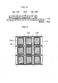
- Fig. 6 is a plane view of a substrate formed before sawing in a method of fabricating an organic light emitting display according to an embodiment of the present invention.
- the organic light emitting diode 190 and the driver circuit 139 are arranged on the substrate 110 in the form of a matrix.
- the organic light emitting diode 190 and the driver circuit 139 are defined as the unit.
- the unit is arranged in a 3 ⁇ 3 matrix in Fig. 6 .
- the present invention is not limited thereto.
- the encapsulant 240 in the form of a square band is formed on the outer periphery of the respective unit.
- the encapsulation substrate is seated on the encapsulant 240.
- the encapsulation substrate has been omitted in Fig. 6 .
- the bonding agent 260 is formed on the under surface of the substrate 110 so as to bond with another substrate. As shown, the bonding agent 260 is formed in the horizontal direction. However, the present invention is not restricted to this pattern. The bonding agent 260 can be formed in the vertical direction or a checkerboard.
- a two-dot chain line defines the sawing line in the drawings. As illustrated in Fig. 6 , the sawing line can be formed in the shape of a checkerboard.
- the bonding agent 260 is formed in the horizontal direction along one side of the sawing line.
- the bonding agent 260 with a predetermined thickness is left on one side end of the substrate 110.
- the position of the bonding agent 260 left on the substrate 110 varies according to the forming position of the bonding agent 260. If the bonding agent 260 is formed along the sawing line with a state that the width of the bonding agent 260 is wider than that of the sawing line, then the bonding agent 260 will remain on every periphery (square periphery) of the sawed substrate 110.
- the bonding agent 260 prevents the organic light emitting display from being bent or damaged by reinforcing the rigidity of the organic light emitting display during the fabricating process or in use, as described above.
- the organic light emitting display formed by the method of the present invention can be easily applied to electronic appliances, such as cellular telephones, Personal Digital Assistants (PDAs), notebook computers, computer monitors and televisions, being made in a thin and compact size, since the organic light emitting display formed by the method according to the present invention is formed on the substrate having a thickness of 0.05 to 1 mm.
- electronic appliances such as cellular telephones, Personal Digital Assistants (PDAs), notebook computers, computer monitors and televisions
- the organic light emitting display formed by the method according to the present invention prevents UV-rays from influencing the semiconductor layer or the organic light emitting diode through the substrate by forming the non-transmissive layer on the substrate.
- the organic light emitting display formed by the method according to the present invention prevents the substrate from being damaged due to external forces as rigidity is increased by forming the bonding agent on one side of the under surface of the substrate.
- the method of fabricating the organic light emitting display according to the present invention can shorten the overall process time by about 50% as the semiconductor process and the organic thin layer process (including cleaning, etching, exposure, development and heat treatment) are executed simultaneously by means of bonding two substrates having a thickness of 0.05 to 1 mm, and prevent the substrate from being bent during the transportation process by obtaining a specific rigidity.
- the fabricating method according to the present invention prevents UV-rays due to the exposure process from influencing the other substrate on the opposite side during of fabricating process by forming the non-transmissive layer on the under surface of the substrate.
- the fabricating method according to the present invention prevents the organic light emitting display from being bent or damaged due to the repulsion force between the magnetic layer and the transporting machine transporting the magnetic layer (since another magnetic layer repulsive to the magnetic layer is formed on the transporting machine) or the force of gravity during fabricating process as rigidity is increased by forming the non-transmissive layer/magnetic layer on the under surface of the substrate.
- the fabricating method according to the present invention prevents the substrates from contacting each other, and thus, from being damaged by forming the non-transmissive layer/magnetic layer/anti-friction layer or the non-transmissive layer/anti-friction layer on the under surface of the substrate.
Landscapes
- Physics & Mathematics (AREA)
- Optics & Photonics (AREA)
- Engineering & Computer Science (AREA)
- Manufacturing & Machinery (AREA)
- Electroluminescent Light Sources (AREA)
- Devices For Indicating Variable Information By Combining Individual Elements (AREA)
Claims (20)
- Procédé de fabrication d'un affichage électroluminescent organique, comprenant :la formation d'une couche non transmissive (210) sur une surface inférieure de chacun de deux substrats (110) ;la liaison des deux substrats (110) en leur appliquant un agent de liaison (260), de telle sorte que les couches non transmissives (210) soient face à face ;la formation d'une couche semi-conductrice (130) sur chaque surface supérieure respective des substrats liés (110), opposée à l'opposé de la couche non transmissive (210) ;la formation d'une diode électroluminescente organique (190) sur chaque couche semi-conductrice respective (130) ;après formation des diodes électroluminescentes organiques (190), la mise en place d'un substrat d'encapsulation (250) sur la surface supérieure de chaque substrat (110), en appliquant un encapsulant (240) sur leur surface supérieure ;après mise en place des substrats d'encapsulation (250), le sciage de la région des deux substrats liés (110) correspondant à une périphérie externe de l'encapsulant (240) alors que les deux substrats (110) sont maintenus ensemble par l'agent de liaison (260) ; etaprès le sciage, la séparation des deux substrats liés (110).
- Procédé de fabrication d'un affichage électroluminescent organique selon la revendication 1, dans lequel la liaison des substrats (110) comprend l'utilisation de l'un adhésif époxy ou d'un adhésif durcissant aux UV comme agent de liaison (260).
- Procédé de fabrication d'un affichage électroluminescent organique selon la revendication 1 ou 2, dans lequel la liaison des substrats (110) comprend l'application de l'agent de liaison (260) sur les bords du substrat (110).
- Procédé de fabrication d'un affichage électroluminescent organique selon l'une quelconque des revendications précédentes, dans lequel la liaison des substrats (110) comprend l'application de l'agent de liaison (260) sur une région de la surface inférieure du substrat (110) à une position correspondant à une périphérie externe de la couche semi-conductrice (130) et de la diode électroluminescente organique (190).
- Procédé de fabrication d'un affichage électroluminescent organique selon l'une quelconque des revendications précédentes, dans lequel la liaison des substrats (110) comprend l'application de l'agent de liaison (260) sur une région de la surface inférieure du substrat (110) à une position correspondant à une périphérie externe de l'encapsulant (240).
- Procédé de fabrication d'un affichage électroluminescent organique selon l'une quelconque des revendications précédentes, dans lequel les substrats (110) ont une épaisseur dans une plage de 0,05 à 1 mm.
- Procédé de fabrication d'un affichage électroluminescent organique selon l'une quelconque des revendications précédentes, dans lequel les substrats (110) comprennent un verre, un plastique, un polymère ou un acier.
- Procédé de fabrication d'un affichage électroluminescent organique selon l'une quelconque des revendications précédentes, comprenant en outre la formation de la couche non transmissive (210) de sorte qu'elle ait une épaisseur dans une plage de 500 à 3000 Å.
- Procédé de fabrication d'un affichage électroluminescent organique selon l'une quelconque des revendications précédentes, comprenant en outre la formation de la couche non transmissive (210) par formation d'un revêtement comprenant l'un d'un métal par lequel les rayons UV sont bloqués, d'un agent anti-UV transparent ou d'un agent anti-UV opaque.
- Procédé de fabrication d'un affichage électroluminescent organique selon l'une quelconque des revendications précédentes, comprenant en outre la formation de la couche non transmissive (210) à partir de l'un d'un Cr, Cr2O3, Al, Au, Ag, MgO ou d'un alliage d'argent.
- Procédé de fabrication d'un affichage électroluminescent organique selon l'une quelconque des revendications précédentes, comprenant en outre la formation d'une couche magnétique (220) sur la surface inférieure de la couche non transmissive (210).
- Procédé de fabrication d'un affichage électroluminescent organique selon la revendication 11, comprenant en outre une couche anti-friction (230) sur une surface inférieure de la couche magnétique (220).
- Procédé de fabrication d'un affichage électroluminescent organique selon l'une quelconque des revendications 1 à 10, comprenant en outre la formation d'une couche anti-friction (230) sur la surface inférieure de la couche non transmissive (210).
- Procédé de fabrication d'un affichage électroluminescent organique selon l'une quelconque des revendications 12 ou 13, dans lequel la formation de la couche anti-friction (230) comprend en outre la formation d'une couche anti-friction ayant une épaisseur dans une plage de 10 à 100 µm.
- Procédé de fabrication d'un affichage électroluminescent organique selon l'une quelconque des revendications 12 à 14, dans lequel la formation de la couche anti-friction (230) comprend en outre la formation d'une couche anti-friction à partir d'un matériau organique ou bien d'un matériau inorganique.
- Procédé de fabrication d'un affichage électroluminescent organique selon l'une quelconque des revendications 12 à 15, dans lequel l'étape de liaison des substrats comprend la formation de couches anti-friction (230) sur les substrats respectifs de sorte qu'elles soient en contact les unes avec les autres.
- Procédé de fabrication d'un affichage électroluminescent organique selon l'une quelconque des revendications précédentes, dans lequel la mise en place du substrat d'encapsulation (250) comprend la formation de la zone du substrat d'encapsulation (250) de sorte qu'elle soit plus petite que celle du substrat (110).
- Procédé de fabrication d'un affichage électroluminescent organique selon l'une quelconque des revendications précédentes, dans lequel le sciage est réalisé au moyen d'un faisceau laser.
- Procédé de fabrication d'un affichage électroluminescent organique selon l'une quelconque des revendications précédentes, comprenant en outre le retrait de la couche non transmissive (210) après séparation des substrats (110).
- Procédé de fabrication d'un affichage électroluminescent organique selon l'une quelconque des revendications précédentes, comprenant en outre la formation d'un circuit d'attaque d'un côté de la couche semi-conductrice (130) après formation de la couche semi-conductrice (130).
Applications Claiming Priority (1)
| Application Number | Priority Date | Filing Date | Title |
|---|---|---|---|
| KR1020060120208A KR100833738B1 (ko) | 2006-11-30 | 2006-11-30 | 유기 전계 발광 표시 장치 및 그 제조 방법 |
Publications (2)
| Publication Number | Publication Date |
|---|---|
| EP1928041A1 EP1928041A1 (fr) | 2008-06-04 |
| EP1928041B1 true EP1928041B1 (fr) | 2014-04-16 |
Family
ID=39111551
Family Applications (1)
| Application Number | Title | Priority Date | Filing Date |
|---|---|---|---|
| EP07252153.7A Not-in-force EP1928041B1 (fr) | 2006-11-30 | 2007-05-25 | Procédé de fabrication d'un affichage électroluminescent organique |
Country Status (5)
| Country | Link |
|---|---|
| US (2) | US8148719B2 (fr) |
| EP (1) | EP1928041B1 (fr) |
| JP (1) | JP4713534B2 (fr) |
| KR (1) | KR100833738B1 (fr) |
| CN (1) | CN101192652B (fr) |
Families Citing this family (21)
| Publication number | Priority date | Publication date | Assignee | Title |
|---|---|---|---|---|
| KR100824880B1 (ko) * | 2006-11-10 | 2008-04-23 | 삼성에스디아이 주식회사 | 유기 전계 발광 표시 장치 및 그 제조 방법 |
| KR100770127B1 (ko) * | 2006-11-10 | 2007-10-24 | 삼성에스디아이 주식회사 | 유기 전계 발광 표시 장치 및 그 제조 방법 |
| KR100824881B1 (ko) * | 2006-11-10 | 2008-04-23 | 삼성에스디아이 주식회사 | 유기 전계 발광 표시 장치 및 그 제조 방법 |
| KR100833738B1 (ko) | 2006-11-30 | 2008-05-29 | 삼성에스디아이 주식회사 | 유기 전계 발광 표시 장치 및 그 제조 방법 |
| KR100824902B1 (ko) * | 2006-12-13 | 2008-04-23 | 삼성에스디아이 주식회사 | 유기 전계 발광 표시 장치 및 그 제조 방법 |
| KR101084263B1 (ko) * | 2009-12-14 | 2011-11-16 | 삼성모바일디스플레이주식회사 | 유기 발광 표시 장치 |
| US20140139985A1 (en) * | 2012-11-12 | 2014-05-22 | Industrial Technology Research Institute | Environmental sensitive electronic device package |
| CN104183708A (zh) * | 2013-05-21 | 2014-12-03 | 海洋王照明科技股份有限公司 | 一种有机电致发光器件及其制备方法 |
| JP6196086B2 (ja) * | 2013-07-19 | 2017-09-13 | 株式会社小糸製作所 | 有機elパネルおよび車両用灯具 |
| DE102014103747B4 (de) * | 2014-03-19 | 2024-06-13 | Osram Oled Gmbh | Optoelektronisches Bauelement und Verfahren zum Herstellen eines optoelektronischen Bauelements |
| KR20150111005A (ko) * | 2014-03-24 | 2015-10-05 | 삼성디스플레이 주식회사 | 유기 발광 표시 장치 및 그 제조방법 |
| WO2016073549A1 (fr) * | 2014-11-05 | 2016-05-12 | Corning Incorporated | Articles en verre avec des caractéristiques non-planes et éléments de verre sans alcali |
| CN104362259B (zh) * | 2014-11-17 | 2017-02-22 | 京东方科技集团股份有限公司 | 发光二极管显示面板及其封装方法 |
| KR102316211B1 (ko) * | 2014-11-24 | 2021-10-22 | 삼성디스플레이 주식회사 | 유기 발광 표시 장치 |
| CN105607323A (zh) * | 2016-01-04 | 2016-05-25 | 京东方科技集团股份有限公司 | 显示面板和显示装置 |
| JP6727843B2 (ja) * | 2016-02-25 | 2020-07-22 | 株式会社ジャパンディスプレイ | 表示装置 |
| TWI613630B (zh) * | 2016-12-30 | 2018-02-01 | 友達光電股份有限公司 | 可撓性顯示裝置 |
| US20180315808A1 (en) * | 2017-04-28 | 2018-11-01 | Shenzhen China Star Optoelectronics Technology Co., Ltd. | Organic light emitting (oled) display panels, and the manufacturing methods and display devices thereof |
| WO2019049274A1 (fr) | 2017-09-07 | 2019-03-14 | 堺ディスプレイプロダクト株式会社 | Dispositif d'affichage |
| KR102552930B1 (ko) | 2018-06-27 | 2023-07-07 | 삼성디스플레이 주식회사 | 패널 하부 부재 및 이를 포함하는 표시 장치 |
| CN109148716B (zh) * | 2018-08-14 | 2020-05-05 | 武汉华星光电半导体显示技术有限公司 | 一种柔性oled显示面板的制备方法及其母板结构 |
Citations (1)
| Publication number | Priority date | Publication date | Assignee | Title |
|---|---|---|---|---|
| JP2000150145A (ja) * | 1998-11-02 | 2000-05-30 | Toyota Motor Corp | El素子の密封方法 |
Family Cites Families (75)
| Publication number | Priority date | Publication date | Assignee | Title |
|---|---|---|---|---|
| JPS5917810B2 (ja) | 1975-06-12 | 1984-04-24 | セイコーエプソン株式会社 | 回路基板の製造方法 |
| JPS5917810A (ja) | 1982-07-21 | 1984-01-30 | 株式会社東芝 | ガス絶縁母線装置 |
| AU572615B2 (en) * | 1983-12-27 | 1988-05-12 | Sony Corporation | Electrically conductive adhesive sheet circuit board and electrical connection structure |
| US5504605A (en) * | 1993-06-02 | 1996-04-02 | Hitachi, Ltd. | Liquid crystal display module having cut-away portions of the back frame for weight reduction and heat dissipation |
| JP3364081B2 (ja) | 1995-02-16 | 2003-01-08 | 株式会社半導体エネルギー研究所 | 半導体装置の作製方法 |
| JPH0980476A (ja) * | 1995-09-12 | 1997-03-28 | Nec Corp | アクティブマトリックス基板とその製造方法 |
| JPH09211482A (ja) | 1996-01-31 | 1997-08-15 | Sharp Corp | 液晶表示装置 |
| US5986401A (en) * | 1997-03-20 | 1999-11-16 | The Trustee Of Princeton University | High contrast transparent organic light emitting device display |
| CA2353506A1 (fr) * | 1998-11-02 | 2000-05-11 | 3M Innovative Properties Company | Oxydes conducteurs transparents pour ecran plat en plastique |
| JP2000298264A (ja) | 1999-04-13 | 2000-10-24 | Samukon:Kk | 液晶表示装置用ガラス基板の製造方法とそれを用いた液晶表示装置 |
| US6559594B2 (en) * | 2000-02-03 | 2003-05-06 | Semiconductor Energy Laboratory Co., Ltd. | Light-emitting device |
| JP2001267578A (ja) * | 2000-03-17 | 2001-09-28 | Sony Corp | 薄膜半導体装置及びその製造方法 |
| US7083863B2 (en) * | 2001-02-21 | 2006-08-01 | Matsushita Electric Industrial Co., Ltd. | Luminous element and method for preparation thereof |
| JP2002350833A (ja) | 2001-05-30 | 2002-12-04 | Matsushita Electric Ind Co Ltd | 液晶表示装置およびその製造方法 |
| US6735982B2 (en) * | 2001-07-12 | 2004-05-18 | Intel Corporation | Processing relatively thin glass sheets |
| KR100782937B1 (ko) | 2001-07-24 | 2007-12-07 | 엘지.필립스 엘시디 주식회사 | 유기전계발광소자 |
| US6660547B2 (en) * | 2001-07-26 | 2003-12-09 | Osram Opto Semiconductors Gmbh | Stabilization for thin substrates |
| FR2829723B1 (fr) * | 2001-09-14 | 2004-02-20 | Saint Gobain | Vitrage de securite fonctionnalise |
| TW594947B (en) * | 2001-10-30 | 2004-06-21 | Semiconductor Energy Lab | Semiconductor device and method of manufacturing the same |
| US6731064B2 (en) * | 2001-11-20 | 2004-05-04 | International Business Machines Corporation | Yield enchancement pixel structure for active matrix organic light-emitting diode displays |
| KR100483988B1 (ko) * | 2001-11-29 | 2005-04-15 | 삼성에스디아이 주식회사 | 투명도전막의 투과도 변형방법 |
| JP2003173872A (ja) | 2001-12-06 | 2003-06-20 | Sony Corp | アライメント方法、パターン形成方法及びアライメント装置、並びに有機エレクトロルミネッセンス表示装置及びその製造方法 |
| KR100491143B1 (ko) | 2001-12-26 | 2005-05-24 | 삼성에스디아이 주식회사 | 블랙매트릭스를 구비한 평판표시장치 및 그 제조방법 |
| US6815723B2 (en) * | 2001-12-28 | 2004-11-09 | Semiconductor Energy Laboratory Co., Ltd. | Light emitting device, method of manufacturing the same, and manufacturing apparatus therefor |
| US6953735B2 (en) * | 2001-12-28 | 2005-10-11 | Semiconductor Energy Laboratory Co., Ltd. | Method for fabricating a semiconductor device by transferring a layer to a support with curvature |
| KR100845557B1 (ko) | 2002-02-20 | 2008-07-10 | 삼성전자주식회사 | 액티브 매트릭스형 유기전계발광 표시장치 및 그 제조방법 |
| JP2003282235A (ja) | 2002-03-25 | 2003-10-03 | Sanyo Electric Co Ltd | 有機エレクトロルミネッセンス表示装置 |
| TW595254B (en) | 2002-03-29 | 2004-06-21 | Sanyo Electric Co | Electroluminescense display device |
| TWI272641B (en) * | 2002-07-16 | 2007-02-01 | Semiconductor Energy Lab | Method of manufacturing a semiconductor device |
| KR101079757B1 (ko) * | 2002-10-30 | 2011-11-04 | 가부시키가이샤 한도오따이 에네루기 켄큐쇼 | 반도체장치 및 반도체장치의 제작방법 |
| JP2004170910A (ja) | 2002-10-31 | 2004-06-17 | Seiko Epson Corp | 電気光学装置及び電子機器 |
| JP2004192969A (ja) * | 2002-12-12 | 2004-07-08 | Hitachi Displays Ltd | 有機el表示装置 |
| JP4218338B2 (ja) | 2002-12-24 | 2009-02-04 | セイコーエプソン株式会社 | 液晶表示装置の製造方法 |
| KR100904523B1 (ko) * | 2002-12-26 | 2009-06-25 | 엘지디스플레이 주식회사 | 액티브 매트릭스형 유기전계발광 소자용 박막트랜지스터 |
| JP4373085B2 (ja) * | 2002-12-27 | 2009-11-25 | 株式会社半導体エネルギー研究所 | 半導体装置の作製方法、剥離方法及び転写方法 |
| TW578441B (en) * | 2003-01-10 | 2004-03-01 | Au Optronics Corp | Top emission active matrix OLED and fabricating method thereof |
| WO2004075607A1 (fr) | 2003-02-20 | 2004-09-02 | Fujitsu Limited | Element electroluminescent organique et son procede de production |
| US7304005B2 (en) * | 2003-03-17 | 2007-12-04 | Semiconductor Energy Laboratory Co., Ltd. | Laser irradiation apparatus, laser irradiation method, and method for manufacturing a semiconductor device |
| JP2004311421A (ja) * | 2003-03-27 | 2004-11-04 | Sanyo Electric Co Ltd | 有機エレクトロルミネッセンス素子 |
| US7365442B2 (en) * | 2003-03-31 | 2008-04-29 | Osram Opto Semiconductors Gmbh | Encapsulation of thin-film electronic devices |
| US7247986B2 (en) * | 2003-06-10 | 2007-07-24 | Samsung Sdi. Co., Ltd. | Organic electro luminescent display and method for fabricating the same |
| KR20040106808A (ko) | 2003-06-11 | 2004-12-18 | 삼성에스디아이 주식회사 | 평판 표시 장치 |
| KR100527195B1 (ko) | 2003-07-25 | 2005-11-08 | 삼성에스디아이 주식회사 | 유기전계 발광표시장치 |
| KR100542997B1 (ko) * | 2003-08-07 | 2006-01-20 | 삼성에스디아이 주식회사 | 평판표시장치 및 그의 제조방법 |
| JP4373159B2 (ja) | 2003-08-21 | 2009-11-25 | 株式会社半導体エネルギー研究所 | 発光装置 |
| JP2005071646A (ja) * | 2003-08-28 | 2005-03-17 | Chi Mei Electronics Corp | 有機elディスプレイおよびその製造方法 |
| JP2005077945A (ja) * | 2003-09-02 | 2005-03-24 | Toshiba Matsushita Display Technology Co Ltd | 表示装置の製造方法 |
| JP2005085705A (ja) | 2003-09-10 | 2005-03-31 | Seiko Epson Corp | 電気デバイス及びその製造方法、電子機器 |
| KR20050029826A (ko) | 2003-09-23 | 2005-03-29 | 삼성에스디아이 주식회사 | 평판표시장치 및 그의 제조방법 |
| JP4497881B2 (ja) * | 2003-09-30 | 2010-07-07 | 三洋電機株式会社 | 有機el素子および有機elパネル |
| JP2005135977A (ja) * | 2003-10-28 | 2005-05-26 | Renesas Technology Corp | 半導体装置の製造方法及び半導体製造装置 |
| KR100959786B1 (ko) | 2003-12-23 | 2010-05-28 | 엘지디스플레이 주식회사 | 유기전계발광소자의 제조방법 |
| JP3646120B1 (ja) | 2004-02-05 | 2005-05-11 | 西山ステンレスケミカル株式会社 | 有機エレクトロルミネッセンスディスプレイ(以下、有機eld)パネルの製造方法、および、有機eldパネル用ガラス基板の薄型化方法 |
| GB0406540D0 (en) | 2004-03-24 | 2004-04-28 | Koninkl Philips Electronics Nv | Electroluminescent display devices |
| KR100615214B1 (ko) | 2004-03-29 | 2006-08-25 | 삼성에스디아이 주식회사 | 평판 디스플레이 장치 |
| KR100984362B1 (ko) * | 2004-04-02 | 2010-09-30 | 삼성전자주식회사 | 유기 발광 표시판 |
| JP2005340182A (ja) * | 2004-04-30 | 2005-12-08 | Toyota Industries Corp | El装置の基板の薄型化方法及び貼り合わせ基板の分断方法 |
| KR20050112031A (ko) | 2004-05-24 | 2005-11-29 | 삼성에스디아이 주식회사 | 반도체 소자 및 그 형성 방법 |
| JP2005340011A (ja) | 2004-05-27 | 2005-12-08 | Seiko Epson Corp | 電気光学装置及び電子機器 |
| KR100603350B1 (ko) * | 2004-06-17 | 2006-07-20 | 삼성에스디아이 주식회사 | 전계 발광 디스플레이 장치 |
| JP2006058814A (ja) | 2004-08-24 | 2006-03-02 | Sony Corp | 表示装置 |
| JP2005222930A (ja) * | 2004-12-15 | 2005-08-18 | Nishiyama Stainless Chem Kk | 有機エレクトロルミネッセンスディスプレイパネルの製造方法、および、有機エレクトロルミネッセンスディスプレイパネル用ガラス基板の薄型化方法 |
| JP2006216456A (ja) | 2005-02-04 | 2006-08-17 | Seiko Instruments Inc | 有機電子デバイスの製造方法 |
| KR20050051646A (ko) | 2005-02-18 | 2005-06-01 | 후지쯔 가부시끼가이샤 | 유기 el 소자 및 그 제조 방법 |
| KR100700657B1 (ko) | 2005-03-14 | 2007-03-27 | 삼성에스디아이 주식회사 | 유기 전계 발광 표시 장치 |
| JP2006270511A (ja) | 2005-03-24 | 2006-10-05 | Fuji Xerox Co Ltd | 情報処理装置、データ送信方法および情報処理プログラム |
| KR20060124940A (ko) | 2005-06-01 | 2006-12-06 | 삼성전자주식회사 | 가요성 표시 장치의 제조 방법 |
| KR100711890B1 (ko) | 2005-07-28 | 2007-04-25 | 삼성에스디아이 주식회사 | 유기 발광표시장치 및 그의 제조방법 |
| JP4466536B2 (ja) | 2005-10-26 | 2010-05-26 | パナソニック電工株式会社 | 照明装置 |
| KR100742368B1 (ko) | 2005-11-02 | 2007-07-24 | 삼성에스디아이 주식회사 | 유기전계발광소자 및 그 제조방법 |
| KR100824881B1 (ko) * | 2006-11-10 | 2008-04-23 | 삼성에스디아이 주식회사 | 유기 전계 발광 표시 장치 및 그 제조 방법 |
| KR100824880B1 (ko) * | 2006-11-10 | 2008-04-23 | 삼성에스디아이 주식회사 | 유기 전계 발광 표시 장치 및 그 제조 방법 |
| KR100770127B1 (ko) * | 2006-11-10 | 2007-10-24 | 삼성에스디아이 주식회사 | 유기 전계 발광 표시 장치 및 그 제조 방법 |
| KR100833738B1 (ko) | 2006-11-30 | 2008-05-29 | 삼성에스디아이 주식회사 | 유기 전계 발광 표시 장치 및 그 제조 방법 |
| KR100824902B1 (ko) * | 2006-12-13 | 2008-04-23 | 삼성에스디아이 주식회사 | 유기 전계 발광 표시 장치 및 그 제조 방법 |
-
2006
- 2006-11-30 KR KR1020060120208A patent/KR100833738B1/ko not_active Expired - Fee Related
-
2007
- 2007-04-13 US US11/785,043 patent/US8148719B2/en not_active Expired - Fee Related
- 2007-04-18 JP JP2007109768A patent/JP4713534B2/ja not_active Expired - Fee Related
- 2007-04-20 CN CN2007100978669A patent/CN101192652B/zh not_active Expired - Fee Related
- 2007-05-25 EP EP07252153.7A patent/EP1928041B1/fr not_active Not-in-force
-
2012
- 2012-02-29 US US13/408,919 patent/US8580588B2/en not_active Expired - Fee Related
Patent Citations (1)
| Publication number | Priority date | Publication date | Assignee | Title |
|---|---|---|---|---|
| JP2000150145A (ja) * | 1998-11-02 | 2000-05-30 | Toyota Motor Corp | El素子の密封方法 |
Also Published As
| Publication number | Publication date |
|---|---|
| US8148719B2 (en) | 2012-04-03 |
| EP1928041A1 (fr) | 2008-06-04 |
| CN101192652A (zh) | 2008-06-04 |
| CN101192652B (zh) | 2010-06-16 |
| JP4713534B2 (ja) | 2011-06-29 |
| US20120156813A1 (en) | 2012-06-21 |
| JP2008141151A (ja) | 2008-06-19 |
| KR100833738B1 (ko) | 2008-05-29 |
| US20080128683A1 (en) | 2008-06-05 |
| US8580588B2 (en) | 2013-11-12 |
Similar Documents
| Publication | Publication Date | Title |
|---|---|---|
| US8148719B2 (en) | Organic light emitting display device and fabricating method thereof | |
| EP1933401B1 (fr) | Affichage électroluminescent organique et son procédé de fabrication | |
| JP4465367B2 (ja) | 有機電界発光表示装置及びその製造方法 | |
| EP1921679B1 (fr) | Affichage électroluminescent organique et son procédé de fabrication | |
| US8536567B2 (en) | Organic light emitting display and fabrication method thereof | |
| EP1906467A2 (fr) | Affichage électroluminescent organique et son procédé de fabrication, et son dispositif de déplacement |
Legal Events
| Date | Code | Title | Description |
|---|---|---|---|
| PUAI | Public reference made under article 153(3) epc to a published international application that has entered the european phase |
Free format text: ORIGINAL CODE: 0009012 |
|
| 17P | Request for examination filed |
Effective date: 20070601 |
|
| AK | Designated contracting states |
Kind code of ref document: A1 Designated state(s): AT BE BG CH CY CZ DE DK EE ES FI FR GB GR HU IE IS IT LI LT LU LV MC MT NL PL PT RO SE SI SK TR |
|
| AX | Request for extension of the european patent |
Extension state: AL BA HR MK RS |
|
| AKX | Designation fees paid |
Designated state(s): DE FR GB HU |
|
| RAP1 | Party data changed (applicant data changed or rights of an application transferred) |
Owner name: SAMSUNG MOBILE DISPLAY CO., LTD. |
|
| 17Q | First examination report despatched |
Effective date: 20121025 |
|
| RAP1 | Party data changed (applicant data changed or rights of an application transferred) |
Owner name: SAMSUNG DISPLAY CO., LTD. |
|
| GRAP | Despatch of communication of intention to grant a patent |
Free format text: ORIGINAL CODE: EPIDOSNIGR1 |
|
| RIC1 | Information provided on ipc code assigned before grant |
Ipc: H01L 51/52 20060101AFI20131009BHEP Ipc: H01L 51/56 20060101ALI20131009BHEP |
|
| INTG | Intention to grant announced |
Effective date: 20131107 |
|
| GRAS | Grant fee paid |
Free format text: ORIGINAL CODE: EPIDOSNIGR3 |
|
| GRAA | (expected) grant |
Free format text: ORIGINAL CODE: 0009210 |
|
| AK | Designated contracting states |
Kind code of ref document: B1 Designated state(s): DE FR GB HU |
|
| REG | Reference to a national code |
Ref country code: GB Ref legal event code: FG4D |
|
| REG | Reference to a national code |
Ref country code: DE Ref legal event code: R096 Ref document number: 602007036098 Country of ref document: DE Effective date: 20140528 |
|
| REG | Reference to a national code |
Ref country code: DE Ref legal event code: R097 Ref document number: 602007036098 Country of ref document: DE |
|
| PLBE | No opposition filed within time limit |
Free format text: ORIGINAL CODE: 0009261 |
|
| STAA | Information on the status of an ep patent application or granted ep patent |
Free format text: STATUS: NO OPPOSITION FILED WITHIN TIME LIMIT |
|
| 26N | No opposition filed |
Effective date: 20150119 |
|
| REG | Reference to a national code |
Ref country code: FR Ref legal event code: PLFP Year of fee payment: 9 |
|
| REG | Reference to a national code |
Ref country code: DE Ref legal event code: R097 Ref document number: 602007036098 Country of ref document: DE Effective date: 20150119 |
|
| PGFP | Annual fee paid to national office [announced via postgrant information from national office to epo] |
Ref country code: GB Payment date: 20150422 Year of fee payment: 9 Ref country code: DE Payment date: 20150422 Year of fee payment: 9 |
|
| PGFP | Annual fee paid to national office [announced via postgrant information from national office to epo] |
Ref country code: FR Payment date: 20150422 Year of fee payment: 9 |
|
| PG25 | Lapsed in a contracting state [announced via postgrant information from national office to epo] |
Ref country code: HU Free format text: LAPSE BECAUSE OF FAILURE TO SUBMIT A TRANSLATION OF THE DESCRIPTION OR TO PAY THE FEE WITHIN THE PRESCRIBED TIME-LIMIT; INVALID AB INITIO Effective date: 20070525 |
|
| REG | Reference to a national code |
Ref country code: DE Ref legal event code: R119 Ref document number: 602007036098 Country of ref document: DE |
|
| GBPC | Gb: european patent ceased through non-payment of renewal fee |
Effective date: 20160525 |
|
| REG | Reference to a national code |
Ref country code: FR Ref legal event code: ST Effective date: 20170131 |
|
| PG25 | Lapsed in a contracting state [announced via postgrant information from national office to epo] |
Ref country code: DE Free format text: LAPSE BECAUSE OF NON-PAYMENT OF DUE FEES Effective date: 20161201 Ref country code: FR Free format text: LAPSE BECAUSE OF NON-PAYMENT OF DUE FEES Effective date: 20160531 |
|
| PG25 | Lapsed in a contracting state [announced via postgrant information from national office to epo] |
Ref country code: GB Free format text: LAPSE BECAUSE OF NON-PAYMENT OF DUE FEES Effective date: 20160525 |