EP1930909A2 - Resistiver Multibitspeicher - Google Patents
Resistiver Multibitspeicher Download PDFInfo
- Publication number
- EP1930909A2 EP1930909A2 EP07023356A EP07023356A EP1930909A2 EP 1930909 A2 EP1930909 A2 EP 1930909A2 EP 07023356 A EP07023356 A EP 07023356A EP 07023356 A EP07023356 A EP 07023356A EP 1930909 A2 EP1930909 A2 EP 1930909A2
- Authority
- EP
- European Patent Office
- Prior art keywords
- bit
- phase change
- memory cell
- resistive memory
- inverted
- Prior art date
- Legal status (The legal status is an assumption and is not a legal conclusion. Google has not performed a legal analysis and makes no representation as to the accuracy of the status listed.)
- Withdrawn
Links
Images



Classifications
-
- G—PHYSICS
- G11—INFORMATION STORAGE
- G11C—STATIC STORES
- G11C13/00—Digital stores characterised by the use of storage elements not covered by groups G11C11/00, G11C23/00, or G11C25/00
- G11C13/0002—Digital stores characterised by the use of storage elements not covered by groups G11C11/00, G11C23/00, or G11C25/00 using resistive RAM [RRAM] elements
- G11C13/0021—Auxiliary circuits
- G11C13/003—Cell access
-
- G—PHYSICS
- G11—INFORMATION STORAGE
- G11C—STATIC STORES
- G11C11/00—Digital stores characterised by the use of particular electric or magnetic storage elements; Storage elements therefor
- G11C11/56—Digital stores characterised by the use of particular electric or magnetic storage elements; Storage elements therefor using storage elements with more than two stable states represented by steps, e.g. of voltage, current, phase, frequency
- G11C11/5678—Digital stores characterised by the use of particular electric or magnetic storage elements; Storage elements therefor using storage elements with more than two stable states represented by steps, e.g. of voltage, current, phase, frequency using amorphous/crystalline phase transition storage elements
-
- G—PHYSICS
- G11—INFORMATION STORAGE
- G11C—STATIC STORES
- G11C13/00—Digital stores characterised by the use of storage elements not covered by groups G11C11/00, G11C23/00, or G11C25/00
- G11C13/0002—Digital stores characterised by the use of storage elements not covered by groups G11C11/00, G11C23/00, or G11C25/00 using resistive RAM [RRAM] elements
- G11C13/0004—Digital stores characterised by the use of storage elements not covered by groups G11C11/00, G11C23/00, or G11C25/00 using resistive RAM [RRAM] elements comprising amorphous/crystalline phase transition cells
-
- G—PHYSICS
- G11—INFORMATION STORAGE
- G11C—STATIC STORES
- G11C13/00—Digital stores characterised by the use of storage elements not covered by groups G11C11/00, G11C23/00, or G11C25/00
- G11C13/0002—Digital stores characterised by the use of storage elements not covered by groups G11C11/00, G11C23/00, or G11C25/00 using resistive RAM [RRAM] elements
- G11C13/0021—Auxiliary circuits
- G11C13/0069—Writing or programming circuits or methods
-
- H—ELECTRICITY
- H10—SEMICONDUCTOR DEVICES; ELECTRIC SOLID-STATE DEVICES NOT OTHERWISE PROVIDED FOR
- H10N—ELECTRIC SOLID-STATE DEVICES NOT OTHERWISE PROVIDED FOR
- H10N70/00—Solid-state devices having no potential barriers, and specially adapted for rectifying, amplifying, oscillating or switching
- H10N70/20—Multistable switching devices, e.g. memristors
- H10N70/231—Multistable switching devices, e.g. memristors based on solid-state phase change, e.g. between amorphous and crystalline phases, Ovshinsky effect
-
- G—PHYSICS
- G11—INFORMATION STORAGE
- G11C—STATIC STORES
- G11C13/00—Digital stores characterised by the use of storage elements not covered by groups G11C11/00, G11C23/00, or G11C25/00
- G11C13/0002—Digital stores characterised by the use of storage elements not covered by groups G11C11/00, G11C23/00, or G11C25/00 using resistive RAM [RRAM] elements
- G11C13/0021—Auxiliary circuits
- G11C13/0069—Writing or programming circuits or methods
- G11C2013/0076—Write operation performed depending on read result
-
- G—PHYSICS
- G11—INFORMATION STORAGE
- G11C—STATIC STORES
- G11C2211/00—Indexing scheme relating to digital stores characterized by the use of particular electric or magnetic storage elements; Storage elements therefor
- G11C2211/56—Indexing scheme relating to G11C11/56 and sub-groups for features not covered by these groups
- G11C2211/564—Miscellaneous aspects
- G11C2211/5641—Multilevel memory having cells with different number of storage levels
-
- G—PHYSICS
- G11—INFORMATION STORAGE
- G11C—STATIC STORES
- G11C2211/00—Indexing scheme relating to digital stores characterized by the use of particular electric or magnetic storage elements; Storage elements therefor
- G11C2211/56—Indexing scheme relating to G11C11/56 and sub-groups for features not covered by these groups
- G11C2211/564—Miscellaneous aspects
- G11C2211/5647—Multilevel memory with bit inversion arrangement
-
- G—PHYSICS
- G11—INFORMATION STORAGE
- G11C—STATIC STORES
- G11C2213/00—Indexing scheme relating to G11C13/00 for features not covered by this group
- G11C2213/70—Resistive array aspects
- G11C2213/78—Array wherein the memory cells of a group share an access device, all the memory cells of the group having a common electrode and the access device being not part of a word line or a bit line driver
-
- G—PHYSICS
- G11—INFORMATION STORAGE
- G11C—STATIC STORES
- G11C2213/00—Indexing scheme relating to G11C13/00 for features not covered by this group
- G11C2213/70—Resistive array aspects
- G11C2213/79—Array wherein the access device being a transistor
-
- Y—GENERAL TAGGING OF NEW TECHNOLOGICAL DEVELOPMENTS; GENERAL TAGGING OF CROSS-SECTIONAL TECHNOLOGIES SPANNING OVER SEVERAL SECTIONS OF THE IPC; TECHNICAL SUBJECTS COVERED BY FORMER USPC CROSS-REFERENCE ART COLLECTIONS [XRACs] AND DIGESTS
- Y10—TECHNICAL SUBJECTS COVERED BY FORMER USPC
- Y10T—TECHNICAL SUBJECTS COVERED BY FORMER US CLASSIFICATION
- Y10T29/00—Metal working
- Y10T29/49—Method of mechanical manufacture
- Y10T29/49002—Electrical device making
Definitions
- Resistive memory utilizes the resistance value of a memory element to store one or more bits of data.
- a memory element programmed to have a high resistance value may represent a logic "1" data bit value
- a memory element programmed to have a low resistance value may represent a logic "0" data bit value.
- the resistance value of the memory element is switched electrically by applying a voltage pulse or a current pulse to the memory element.
- One type of resistive memory is phase change memory. Phase change memory uses a phase change material for the resistive memory element.
- Phase change memories are based on phase change materials that exhibit at least two different states.
- Phase change material may be used in memory cells to store bits of data.
- the states of phase change material may be referred to as amorphous and crystalline states.
- the states may be distinguished because the amorphous state generally exhibits higher resistivity than does the crystalline state.
- the amorphous state involves a more disordered atomic structure, while the crystalline state involves a more ordered lattice.
- Some phase change materials exhibit more than one crystalline state, e.g. a face-centered cubic (FCC) state and a hexagonal closest packing (HCP) state.
- FCC face-centered cubic
- HCP hexagonal closest packing
- Phase change in the phase change materials may be induced reversibly.
- the memory may change from the amorphous state to the crystalline state and from the crystalline state to the amorphous state in response to temperature changes.
- the temperature changes to the phase change material may be achieved by driving current through the phase change material itself, or by driving current through a resistive heater adjacent the phase change material. With both of these methods, controllable heating of the phase change material causes controllable phase change within the phase change material.
- a phase change memory including a memory array having a plurality of memory cells that are made of phase change material may be programmed to store data utilizing the memory states of the phase change material.
- One way to read and write data in such a phase change memory device is to control a current and/or a voltage pulse that is applied to the phase change material.
- the level of current and/or voltage generally corresponds to the temperature induced within the phase change material in each memory cell.
- a phase change memory cell can store multiple bits of data.
- Multi-bit storage in a phase change memory cell can be achieved by programming the phase change material to have intermediate resistance values or states. Cells in such intermediate states have a resistance that lies between the fully crystalline state and the fully amorphous state. If the phase change memory cell is programmed to one of three different resistance levels, 1.5 bits of data per cell can be stored. If the phase change memory cell is programmed to one of four different resistance levels, two bits of data per cell can be stored. If the phase change memory cell is programmed to one of eight resistance levels, three bits of data per cell can be stored. If the phase change memory cell is programmed to one of 16 resistance levels, four bits of data per cell can be stored, and so on.
- phase change memory cell typically, there is a wide distribution of resistance values of a phase change memory cell in the two or more resistance states.
- the time to read the value of a phase change memory cell may be significantly long due to the high resistance of the amorphous state or intermediate states of the phase change material. This significantly long read time leads to slow overall memory operation.
- the memory includes a first multi-bit resistive memory cell and a single bit resistive memory cell.
- the single bit resistive memory cell is for storing a bit indicating whether data stored in the first multi-bit resistive memory cell is inverted.
- Figure 1 is a block diagram illustrating one embodiment of a memory device.
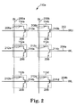
- Figure 2 is a schematic diagram illustrating one embodiment of a memory array.
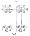
- Figure 3 is a schematic diagram illustrating another embodiment of a memory array.
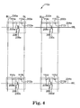
- Figure 4 is a schematic diagram illustrating another embodiment of a memory array.
- Figure 5 is a table illustrating one embodiment of memory cell values for storing three data bits per memory cell.
- Figure 6 is a table illustrating one embodiment of memory cell values for storing four data bits per memory cell.
- Figure 7 is a graph illustrating one embodiment of access time versus measurement accuracy for several memory cell resistance values.
- Figure 1 is a block diagram illustrating one embodiment of a memory device 100.
- Memory device 100 includes a controller 102, a write circuit 106, a memory array 110, and a sense circuit 118.
- Memory array 110 includes multi-bit memory cells 112 and inverted data indicators 114.
- inverted data indicators 114 are single bit memory cells.
- inverted data indicators 114 are multi-bit memory cells.
- each of the multi-bit memory cells 112 and each of the inverted data indicators 114 are phase change memory cells that store data based on the amorphous and crystalline states of phase change material in the memory cell.
- each of the inverted data indicators 114 can be programmed into one of two states by programming the phase change material to one of the amorphous and crystalline states. In another embodiment, each of the inverted data indicators 114 can be programmed into one of three or more state by programming the phase change material to have intermediate resistance values. Each of the multi-bit memory cells 112 can also be programmed into one of three or more states by programming the phase change material to have intermediate resistance values. To program one of multi-bit memory cells 112 or one of inverted data indicators 114 to an intermediate resistance value, the amount of crystalline material coexisting with amorphous material, and hence the cell resistance, is controlled using a suitable write strategy.
- multi-bit memory cells 112 store data in the lower half of the available resistance states. For example, if each multi-bit memory cell 112 stores three data bits, which corresponds to eight resistance states, the lower four resistance states are used. If each multi-bit memory cell 112 stores four data bits, which corresponds to 16 resistance states, the lower eight resistance states are used. The number of resistance states used is reduced by one half by inverting any data that would have been stored in the upper half of the available resistance states and storing the inverted data in the lower half of the available resistance states. By storing the data in the lower half of the available resistance states, the access times for reading the memory cells are reduced.
- each inverted data indicator 114 provides an inversion data bit indicating whether the data stored in a multi-bit memory cell 112 is inverted. In another embodiment, each inverted data indicator 114 provides two or more inversion data bits indicating whether the data stored in two or more respective multi-bit memory cells 112 is inverted.
- a group of multi-bit memory cells 112, such as all multi-bit memory cells 112 along a single bit line, are associated with an inverted data indicator 114.
- the inverted data indicator 114 is a single bit memory cell that indicates whether all the data stored within the group of multi-bit memory cells 112 is inverted.
- up to 50% of the multi-bit memory cells 112 in the group may include data stored in the upper half of the available resistance states. This is a reduction of 50% from the possible 100% of multi-bit memory cells 112 that could include data stored in the upper half of the available resistance states if no data were inverted.
- the inverted data indicator 114 is a multi-bit memory cell that indicates whether the data stored within each respective multi-bit memory cell 112 within the group of multi-bit memory cells 112 is inverted. In this embodiment, the upper half of the available resistance states of the multi-bit memory cells 112 is not used.
- each multi-bit memory cell 112 is paired with an inverted data indicator 114.
- each inverted data indicator 114 is a single bit memory cell that indicates whether the data stored in the multi-bit memory cell 112 is inverted. In this embodiment, the upper half of the available resistance states of the multi-bit memory cells 112 is not used.
- electrically coupled is not meant to mean that the elements must be directly coupled together and intervening elements may be provided between the “electrically coupled” elements.
- Controller 102 is electrically coupled to write circuit 106 through signal path 104 and to sense circuit 118 through signal path 120.
- Write circuit 106 is electrically coupled to memory array 110 though signal path 108.
- Memory array 110 is electrically coupled to sense circuit 118 through signal path 116.
- each of the multi-bit memory cells 112 and each of the inverted data indicators 114 include a phase change material that may be changed from an amorphous state to a crystalline state or from a crystalline state to an amorphous state under the influence of temperature change.
- each inverted data indicator 114 is a single bit memory cell
- the crystalline and amorphous phase change material in one of the single bit memory cells thereby defines two states for storing inversion data within memory array 110.
- each inverted data indicator 114 is a multi-bit memory cell
- the amount of crystalline phase change material coexisting with amorphous phase change material in one of the multi-bit memory cells thereby defines three or more state for storing inversion data within memory array 110.
- the amount of crystalline phase change material coexisting with amorphous phase change material in one of multi-bit memory cells 112 thereby defines three or more states for storing data within memory array 110.
- inverted data indicators 114 are single bit memory cells that include two states and a binary system is used, wherein the two states are assigned bit values of "0" and "1".
- inverted data indicators 114 are multi-bit memory cells that include four states, wherein the four states are assigned bit values of "00", "01", "10", and "11".
- the inverted data indicators 114 can include any suitable number of states.
- multi-bit memory cells 112 include eight states, where only the lower four states are used and are assigned multi-bit values, such as "000”, “001 “, “010”, and “011". Multi-bit values, such as “100”, “101”, “110”, and “111” are inverted and stored as “011”, “010", “001 “, and “000”, respectively.
- the three or more states of multi-bit memory cells 112 can be any suitable number of states in the phase change material of a multi-bit memory cell.
- inverted data indicators 114 are multi-bit memory cells that store fewer bits than multi-bit memory cells 112.
- Controller 102 includes a microprocessor, microcontroller, or other suitable logic circuitry for controlling the operation of memory circuit 100. Controller 102 controls read and write operations of memory circuit 100 including the application of control and data signals to memory array 110 through write circuit 106 and sense circuit 118.
- write circuit 106 provides voltage pulses through signal path 108 to multi-bit memory cells 112 and inverted data indicators 114 to program the memory cells. In other embodiments, write circuit 106 provides current pulses through signal path 108 to multi-bit memory cells 112 and inverted data indicators 114 to program the memory cells.
- Sense circuit 118 reads each of the two or more states of the inverted data indicators 114 and each of the three or more states of the multi-bit memory cells 112 through signal path 116. In one embodiment, to read the resistance of one of the inverted data indicators 114 or one of the multi-bit memory cells 112, sense circuit 118 provides current that flows through one of the inverted data indicators 114 or one of the multi-bit memory cells 112. Sense circuit 118 then reads the voltage across that one of the inverted data indicators 114 or that one of the multi-bit memory cells 112.
- sense circuit 118 provides voltage across one of the inverted data indicators 114 or one of the multi-bit memory cells 112 and reads the current that flows through that one of the inverted data indicators 114 or that one of the multi-bit memory cells 112.
- write circuit 106 provides voltage across one of the inverted data indicators 114 or one of the multi-bit memory cells 112 and sense circuit 118 reads the current that flows through that one of the inverted data indicators 114 or that one of the multi-bit memory cells 112.
- write circuit 106 provides current that flows through one of the inverted data indicators 114 or one of the multi-bit memory cells 112 and sense circuit 118 reads the voltage across that one of the inverted data indicators 114 or that one of the multi-bit memory cells 112.
- write circuit 106 To program an inverted data indicator 114 within memory device 100, write circuit 106 generates a current or voltage pulse for heating the phase change material in the target memory cell. In one embodiment, write circuit 106 generates an appropriate current or voltage pulse, which is distributed to the appropriate target inverted data indicator 114. The current or voltage pulse amplitude and duration is controlled depending on whether the memory cell is being set or reset. Generally, a "set" operation of an inverted data indicator is heating the phase change material of the target memory cell above its crystallization temperature (but below its melting temperature) long enough to achieve the crystalline state or a partially crystalline and partially amorphous state.
- a "reset" operation of an inverted data indicator is heating the phase change material of the target memory cell above its melting temperature, and then quickly quench cooling the material, thereby achieving the amorphous state or a partially amorphous and partially crystalline state.
- write circuit 106 To program a multi-bit memory cell 112 within memory device 100, write circuit 106 generates a current or voltage pulse for heating the phase change material in the target memory cell. In one embodiment, write circuit 106 generates an appropriate current or voltage pulse, which is distributed to the appropriate target multi-bit memory cell 112. The current or voltage pulse amplitude and duration is controlled depending on whether the memory cell is being set or reset. Generally, a "set" operation of a multi-bit memory cell is heating the phase change material of the target memory cell above its crystallization temperature (but below its melting temperature) long enough to achieve the crystalline state or a partially crystalline and partially amorphous state.
- a "reset" operation of a multi-bit memory cell is heating the phase change material of the target memory cell above its melting temperature, and then quickly quench cooling the material, thereby achieving the amorphous state or a partially amorphous and partially crystalline state.
- FIG. 2 is a schematic diagram illustrating one embodiment of a memory array 110a.
- memory array 110 is similar to memory array 110a.
- Memory array 110a includes inverted data indicators 114a-114b, multi-bit phase change memory cells 112a-112d, a plurality of bit lines (BLs) 200a-200b (collectively referred to as bit lines 200), a word line (WLi) for inverted data indicators 114a-114b, and a plurality of word lines (WLs) 204a-204b (collectively referred to as word lines 204) for multi-bit memory cells 112a-112d.
- BLs bit lines
- WLi word line
- word lines 204 word lines
- Each inverted data indicator 114a-114b and each multi-bit phase change memory cell 112a-112d stores data based on the amorphous and crystalline states of phase change material in the memory cell.
- each inverted data indicator 114a-114b is a single bit memory cell that can be programmed into two states by programming the phase change material to the crystalline state or to the amorphous state.
- each inverted data indicator 114a-114b is a multi-bit memory cell that can be programmed into three or more states by programming the phase change material to have intermediate resistance values.
- Each multi-bit memory cell 112a-112d can be programmed into three or more states by programming the phase change material to have intermediate resistance values.
- the amount of crystalline material coexisting with amorphous material, and hence the cell resistance is controlled via a suitable write strategy.
- Each inverted data indicator 114 is electrically coupled to word line 202, a bit line 200, and common or ground 206.
- Inverted data indicator 114a is electrically coupled to bit line 200a, word line 202, and common or ground 206.
- Inverted data indicator 114b is electrically coupled to bit line 200b, word line 202, and common or ground 206.
- Each inverted data indicator 114 includes a phase change element 208 and a transistor 210. While transistor 210 is a field-effect transistor (FET) in the illustrated embodiment, in other embodiments, transistor 210 can be other suitable devices such as a bipolar transistor or a 3D transistor structure. In other embodiments, a diode-like structure may be used in place of transistor 210.
- Inverted data indicator 114a includes phase change element 208a and transistor 210a. One side of phase change element 208a is electrically coupled to bit line 200a, and the other side of phase change element 208a is electrically coupled to one side of the source-drain path of transistor 210a. The other side of the source-drain path of transistor 210a is electrically coupled to common or ground 206. The gate of transistor 210a is electrically coupled to word line 202.
- Inverted data indicator 114b includes phase change element 208b and transistor 210b.
- One side of phase change element 208b is electrically coupled to bit line 200b, and the other side of phase change element 208b is electrically coupled to one side of the source-drain path of transistor 210b.
- the other side of the source-drain path of transistor 210b is electrically coupled to common or ground 206.
- the gate of transistor 210b is electrically coupled to word line 202.
- each phase change element 208a is electrically coupled to common or ground 206 and each transistor 210 is electrically coupled to a bit line 200.
- one side of phase change element 208a is electrically coupled to common or ground 206.
- the other side of phase change element 208a is electrically coupled to one side of the source-drain path of transistor 210a.
- the other side of the source-drain path of transistor 210a is electrically coupled to bit line 200a.
- Each multi-bit phase change memory cell 112 is electrically coupled to a word line 204, a bit line 200, and common or ground 206.
- Phase change memory cell 112a is electrically coupled to bit line 200a, word line 204a, and common or ground 206
- phase change memory cell 112b is electrically coupled to bit line 200a, word line 204b, and common or ground 206.
- Phase change memory cell 112c is electrically coupled to bit line 200b, word line 204a, and common or ground 206
- phase change memory cell 112d is electrically coupled to bit line 200b, word line 204b, and common or ground 206.
- Each phase change memory cell 112 includes a phase change element 212 and a transistor 214. While transistor 214 is a FET in the illustrated embodiment, in other embodiments, transistor 214 can be other suitable devices such as a bipolar transistor or a 3D transistor structure. In other embodiments, a diode-like structure may be used in place of transistor 214.
- Phase change memory cell 112a includes phase change element 212a and transistor 214a. One side of phase change element 212a is electrically coupled to bit line 200a, and the other side of phase change element 212a is electrically coupled to one side of the source-drain path of transistor 214a. The other side of the source-drain path of transistor 214a is electrically coupled to common or ground 206. The gate of transistor 214a is electrically coupled to word line 204a.
- Phase change memory cell 112b includes phase change element 212b and transistor 214b.
- One side of phase change element 212b is electrically coupled to bit line 200a, and the other side of phase change element 212b is electrically coupled to one side of the source-drain path of transistor 214b.
- the other side of the source-drain path of transistor 214b is electrically coupled to common or ground 206.
- the gate of transistor 214b is electrically coupled to word line 204b.
- Phase change memory cell 112c includes phase change element 212c and transistor 214c.
- One side of phase change element 212c is electrically coupled to bit line 200b, and the other side of phase change element 212c is electrically coupled to one side of the source-drain path of transistor 214c.
- the other side of the source-drain path of transistor 214c is electrically coupled to common or ground 206.
- the gate of transistor 214c is electrically coupled to word line 204a.
- Phase change memory cell 112d includes phase change element 212d and transistor 214d.
- One side of phase change element 212d is electrically coupled to bit line 200b, and the other side of phase change element 212d is electrically coupled to one side of the source-drain path of transistor 214d.
- the other side of the source-drain path of transistor 214d is electrically coupled to common or ground 206.
- the gate of transistor 214d is electrically coupled to word line 204b.
- each phase change element 212 is electrically coupled to common or ground 206 and each transistor 214 is electrically coupled to a bit line 200.
- phase change memory cell 112a one side of phase change element 212a is electrically coupled to common or ground 206.
- the other side of phase change element 212a is electrically coupled to one side of the source-drain path of transistor 214a.
- the other side of the source-drain path of transistor 214a is electrically coupled to bit line 200a.
- phase change material of phase change elements 208 and 212 may be made up of a variety of materials in accordance with the present invention. Generally, chalcogenide alloys that contain one or more elements from group VI of the periodic table are useful as such materials.
- the phase change material of phase change elements 208 and 212 is made up of a chalcogenide compound material, such as GeSbTe, SbTe, GeTe, or AgInSbTe.
- the phase change material is chalcogen free, such as GeSb, GaSb, InSb, or GeGaInSb.
- the phase change material is made up of any suitable material including one or more of the elements Ge, Sb, Te, Ga, As, In, Se, and S.
- inverted data indicator 114a is a single bit memory cell that stores a single data bit in phase change element 208a indicating whether the data stored in the multi-bit memory cells 112a-112b along bit line 200a is inverted.
- Inverted data indicator 114b stores a single data bit in phase change element 208b indicating whether the data stored in the multi-bit memory cells 112c-112d along bit line 200b is inverted.
- controller 102 determines whether to invert the data to be stored in the multi-bit memory cells 112 along a bit line 200 so that the number of multi-bit memory cells 112 storing data in the upper half of the available resistance states is less than or equal to the number of multi-bit memory cells 112 storing data in the lower half of the available resistance states.
- inverted data indicator 114a is a multi-bit memory cell that stores more than one data bit in phase change element 208a indicating whether the data stored in each respective multi-bit memory cell 112a-112b along bit line 200a is inverted.
- Inverted data indicator 114b stores more than one data bit in phase change element 208b indicating whether the data stored in each respective multi-bit memory cell 112c-112d along bit line 200b is inverted.
- controller 102 determines whether to invert data to be stored in multi-bit memory cells 112 along a bit line 200 so that no data is stored in the upper half of available resistance states.
- Sense circuit 118 reads the states of inverted data indicators 114a-114b and multi-bit memory cells 112a-112d through bit lines 200a-200b.
- sense circuit 118 provides current that flows through one of the memory cells 114a-114b or 112a-112d through a bit line 200a-200b with the word line 202 or 204 for the memory cell selected.
- Sense circuit 118 then reads the voltage across that one of the memory cells 114a-114b or 112a-112d to determine the resistance state.
- sense circuit 118 provides voltage across one of the memory cells 114a-114b or 112a-112d through a bit line 200a-200b with the word line 202 or 204 for the memory cell selected. Sense circuit 118 then reads the current through that one of the memory cells 114a-114b or 112a-112d to determine the resistance state.
- Sense circuit 118 reads the state of the inverted data indicators 114a-114b for a bit line 200a-200b each time a multi-bit memory cell 112a-112d along the same bit line 200a-200b is read.
- Sense circuit 118 sets the reference level of a sense amplifier coupled to the selected bit line 200a-200b to a first level for sensing the state of the inverted data indicator 114a-114b and to a second level for sensing the state of the multi-bit memory cells 112a-112d.
- inverted data indicators 114a-114b are single bit memory cells.
- phase change element 208a of single bit memory cell 114a being set to "0"
- the data read from phase change elements 212a-212b of multi-bit memory cells 112a-112b is not inverted before being passed to an external circuit.
- phase change element 208a of single bit memory cell 114a being set to "1”
- the data read from phase change elements 212a-212b of multi-bit memory cells 112a-112b is inverted before being passed to an external circuit.
- phase change element 208b of single bit memory cell 114b In response to phase change element 208b of single bit memory cell 114b being set to "0", the data read from phase change elements 212c-212d of multi-bit memory cells 112c-112d is not inverted before being passed to an external circuit. In response to phase change element 208b of single bit memory cell 114b being set to "1", the data read from phase change elements 212c-212d of multi-bit memory cells 112c-112d is inverted before being passed to an external circuit.
- a "1" stored in a single bit memory cell 114a-114b indicates the data stored in the associated multi-bit memory cells 112a-112d is not inverted, and a "0" stored in a single bit memory cell 114a-114b indicates the data stored in the associated multi-bit memory cells 112a-112d is inverted.
- inverted data indicators 114a-114b are multi-bit memory cells.
- phase change element 208a of multi-bit memory cell 114a being set to "00"
- the data read from phase change element 212a of multi-bit memory cell 112a is not inverted and the data read from phase change element 212b of multi-bit memory cell 112b is not inverted before being passed to an external circuit.
- phase change element 208a of multi-bit memory cell 114a being set to "0 1 ", the data read from phase change element 212a of multi-bit memory cell 112a is not inverted and the data read from phase change element 212b of multi-bit memory cell 112b is inverted before being passed to an external circuit.
- phase change element 208a of multi-bit memory cell 114a In response to phase change element 208a of multi-bit memory cell 114a being set to "10", the data read from phase change element 212a of multi-bit memory cell 112a is inverted and the data read from phase change element 212b of multi-bit memory cell 112b is not inverted before being passed to an external circuit. In response to phase change element 208a of multi-bit memory cell 114a being set to "11 ", the data read from phase change element 212a of multi-bit memory cell 112a is inverted and the data read from phase change element 212b of multi-bit memory cell 112b is inverted before being passed to an external circuit.
- Multi-bit memory cell 114b is used similarly to multi-bit memory cell 114a for multi-bit memory cells 112c and 112d along bit line 200b.
- a "11" stored in a multi-bit memory cell 114 indicates the data stored in the associated multi-bit memory cells 112 is not inverted
- a "00" stored in a multi-bit memory cell 114 indicates the data stored in the associated multi-bit memory cells 112 is inverted.
- phase change element 208a reaches the crystalline state or a partially crystalline and partially amorphous state during this set operation.
- a reset current or voltage pulse is selectively enabled and sent through bit line 200a to phase change element 208a. The reset current or voltage quickly heats phase change element 208a above its melting temperature.
- phase change element 208a quickly quench cools into the amorphous state or a partially amorphous and partially crystalline state.
- Inverted data indicator 114b and other inverted data indicators 114 in memory array 110a are set and reset similarly to inverted data indicator 114a using a similar current or voltage pulse.
- phase change element 212a During a set operation of multi-bit phase change memory cell 112a, a set current or voltage pulse is selectively enabled and sent through bit line 200a to phase change element 212a thereby heating it above its crystallization temperature (but usually below its melting temperature) with word line 204a selected to activate transistor 214a. In this way, phase change element 212a reaches its crystalline state or a partially crystalline and partially amorphous state during this set operation.
- a reset current or voltage pulse is selectively enabled and sent through bit line 200a to phase change element 212a. The reset current or voltage quickly heats phase change element 212a above its melting temperature.
- phase change element 212a quickly quench cools into the amorphous state or a partially amorphous and partially crystalline state.
- Phase change memory cells 112b-112d and other phase change memory cells 112 in memory array 110a are set and reset similarly to phase change memory cell 112a using a similar current or voltage pulse.
- FIG. 3 is a schematic diagram illustrating another embodiment of a memory array 110b.
- memory array 110 is similar to memory array 110b.
- Memory array 110b includes inverted data indicators 114a-114d, multi-bit phase change memory cells 112a-112d, a plurality of inverted data indicator bit lines (BLi) 220a-220b, a plurality of multi-bit memory cell bit lines (BLs) 200a-200b, and a plurality of word lines (WLs) 204a-204b.
- BLi inverted data indicator bit lines
- BLs multi-bit memory cell bit lines
- WLs word lines
- Each inverted data indicator 114 is electrically coupled to a word line 204, a bit line 220, and common or ground 206.
- Inverted data indicator 114a is electrically coupled to bit line 220a, word line 204a, and common or ground 206.
- Inverted data indicator 114b is electrically coupled to bit line 220a, word line 204b, and common or ground 206.
- Inverted data indicator 114c is electrically coupled to bit line 220b, word line 204a, and common or ground 206.
- Inverted data indicator 114d is electrically coupled to bit line 220b, word line 204b, and common or ground 206.
- Each multi-bit phase change memory cell 112 is configured as previously described and illustrated with reference to Figure 2 .
- Each inverted data indicator 114 includes a phase change element 208 and a transistor 210.
- Inverted data indicator 114a includes phase change element 208a and transistor 210a.
- One side of phase change element 208a is electrically coupled to bit line 220a, and the other side of phase change element 208a is electrically coupled to one side of the source-drain path of transistor 210a.
- the other side of the source-drain path of transistor 210a is electrically coupled to common or ground 206.
- the gate of transistor 210a is electrically coupled to word line 204a.
- Inverted data indicator 114b includes phase change element 208b and transistor 210b.
- One side of phase change element 208b is electrically coupled to bit line 220a, and the other side of phase change element 208b is electrically coupled to one side of the source-drain path of transistor 210b.
- the other side of the source-drain path of transistor 210b is electrically coupled to common or ground 206.
- the gate of transistor 210b is electrically coupled to word line 204b.
- Inverted data indicator 114c includes phase change element 208c and transistor 210c.
- One side of phase change element 208c is electrically coupled to bit line 220b, and the other side of phase change element 208c is electrically coupled to one side of the source-drain path of transistor 210c.
- the other side of the source-drain path of transistor 210c is electrically coupled to common or ground 206.
- the gate of transistor 210c is electrically coupled to word line 204a.
- Inverted data indicator 114d includes phase change element 208d and transistor 210d.
- One side of phase change element 208d is electrically coupled to bit line 220b, and the other side of phase change element 208d is electrically coupled to one side of the source-drain path of transistor 210d.
- the other side of the source-drain path of transistor 210d is electrically coupled to common or ground 206.
- the gate of transistor 210d is electrically coupled to word line 204b.
- each phase change element 208 is electrically coupled to common or ground 206 and each transistor 210 is electrically coupled to a bit line 220.
- one side of phase change element 208a is electrically coupled to common or ground 206.
- the other side of phase change element 208a is electrically coupled to one side of the source-drain path of transistor 210a.
- the other side of the source-drain path of transistor 210a is electrically coupled to bit line 220a.
- each inverted data indicator 114 is a single bit memory cell that stores a single data bit indicating whether the data stored in the associated multi-bit memory cell 112 is inverted.
- Single bit memory cell 114a stores a single data bit in phase change element 208a indicating whether the data stored in phase change element 212a of multi-bit memory cell 112a is inverted.
- Single bit memory cell 114b stores a single data bit in phase change element 208b indicating whether the data stored in phase change element 212b of multi-bit memory cell 112b is inverted.
- Single bit memory cell 114c stores a single data bit in phase change element 208c indicating whether the data stored in phase change element 212c of multi-bit memory cell 112c is inverted.
- Single bit memory cell 114d stores a single data bit in phase change element 208d indicating whether the data stored in phase change element 212d of multi-bit memory cell 112d is inverted. Controller 102 determines whether to invert the data to be stored in each multi-bit memory cell 112 so that the data is stored in the lower half of the available resistance states within each memory cell 112.
- each inverted data indicator 114 is a multi-bit memory cell that stores more than one data bit indicating whether the data stored in more than one respective associated multi-bit memory cell 112 is inverted.
- multi-bit memory cell 114a can store two bits. The first bit can indicate whether the data stored in multi-bit memory cell 112a is inverted. The second bit can indicate whether the data stored in multi-bit memory cell 112c is inverted.
- inverted data indicator 114c and bit line 220b can be eliminated since they are not used.
- Sense circuit 118 reads the states of inverted data indicators 114a-114d through bit lines 220a-220b. Sense circuit 118 reads the states of multi-bit memory cells 112a-112d through bit lines 200a-200b. In one embodiment, to read the resistance of one of the inverted data indicators 114a-114d sense circuit 118 provides current that flows through one of the memory cells 114a-114d through a bit line 220a-220b with the word line 204 for the memory cell selected. Sense circuit 118 then reads the voltage across that one of the memory cells 114a-114b to determine the resistance state.
- sense circuit 118 provides voltage across one of the memory cells 114a-114d through a bit line 220a-220b with the word line 204 for the memory cell selected. Sense circuit 118 then reads the current through that one of the memory cells 114a-114b to determine the resistance state.
- sense circuit 118 to read the resistance of one of the multi-bit memory cells 112a-112d, sense circuit 118 provides current that flows through one of the memory cells 112a-112d through a bit line 200a-200b with the word line 204 for the memory cell selected. Sense circuit 118 then reads the voltage across that one of the memory cells 112a-112d to determine the resistance state. In another embodiment, sense circuit 118 provides voltage across one of the memory cells 112a-112d through a bit line 200a-200b with the word line 204 for the memory cell selected. Sense circuit 118 then reads the current through that one of the memory cells 112a-112d to determine the resistance state.
- Sense circuit 118 reads the state of an inverted data indicator 114a-114d each time an associated multi-bit memory cell 112a-112d is read. Sense circuit 118 sets the reference levels of sense amplifiers coupled to bit lines 220a-220b to a first level for sensing the state of the inverted data indicators 114a-114d. Sense circuit 118 sets the reference levels of sense amplifiers coupled to bit lines 200a-200b to a second level for sensing the state of the multi-bit memory cells 112a-112d.
- inverted data indicators 114a-114d are single bit memory cells.
- phase change element 208a of single bit memory cell 114a being set to "0"
- the data read from phase change element 212a of multi-bit memory cell 112a is not inverted before being passed to an external circuit.
- phase change element 208a of single bit memory cell 114a being set to "1”
- the data read from phase change element 212a of multi-bit memory cell 112a is inverted before being passed to an external circuit.
- phase change element 208b of single bit memory cell 114b being set to "0”
- the data read from phase change element 212b of multi-bit memory cell 112b is not inverted before being passed to an external circuit.
- phase change element 208b of single bit memory cell 114b being set to "1"
- the data read from phase change element 212b of multi-bit memory cell 112b is inverted before being passed to an external circuit.
- phase change element 208c of single bit memory cell 114c In response to phase change element 208c of single bit memory cell 114c being set to "0", the data read from phase change element 212c of multi-bit memory cell 112c is not inverted before being passed to an external circuit. In response to phase change element 208c of single bit memory cell 114c being set to "1 ", the data read from phase change element 212c of multi-bit memory cell 112c is inverted before being passed to an external circuit. In response to phase change element 208d of single bit memory cell 114d being set to "0", the data read from phase change element 212d of multi-bit memory cell 112d is not inverted before being passed to an external circuit.
- phase change element 208d of single bit memory cell 114d In response to phase change element 208d of single bit memory cell 114d being set to "1", the data read from phase change element 212d of multi-bit memory cell 112d is inverted before being passed to an external circuit.
- a "1" stored in a single bit memory cell 114a-114d indicates the data stored in the associated multi-bit memory cell 112a-112d is not inverted, and a "0" stored in a single bit memory cell 114a-114d indicates the data stored in the associated multi-bit memory cell 112a-112d is inverted.
- inverted data indicators 114a-114d are multi-bit memory cells and inverted data indicators 114c-114d and bit line 220b are excluded.
- phase change element 208a of multi-bit memory cell 114a being set to "00"
- the data read from phase change element 212a of multi-bit memory cell 112a is not inverted and the data read from phase change element 212c of multi-bit memory cell 112c is not inverted before being passed to an external circuit.
- phase change element 208a of multi-bit memory cell 114a In response to phase change element 208a of multi-bit memory cell 114a being set to "01", the data read from phase change element 212a of multi-bit memory cell 112a is not inverted and the data read from phase change element 212c of multi-bit memory cell 112c is inverted before being passed to an external circuit. In response to phase change element 208a of multi-bit memory cell 114a being set to "10", the data read from phase change element 212a of multi-bit memory cell 112a is inverted and the data read from phase change element 212c of multi-bit memory cell 112c is not inverted before being passed to an external circuit.
- phase change element 208a of multi-bit memory cell 114a In response to phase change element 208a of multi-bit memory cell 114a being set to "11", the data read from phase change element 212a of multi-bit memory cell 112a is inverted and the data read from phase change element 212c of multi-bit memory cell 112c is inverted before being passed to an external circuit.
- Multi-bit memory cell 114b is used similarly to multi-bit memory cell 114a for multi-bit memory cells 112b and 112d along word line 204b.
- a "11" stored in a multi-bit memory cell 114 indicates the data stored in the associated multi-bit memory cells 112 is not inverted
- a "00" stored in a multi-bit memory cell 114 indicates the data stored in the associated multi-bit memory cells 112 is inverted.
- phase change element 208a reaches the crystalline state or a partially crystalline and partially amorphous state during this set operation.
- a reset current or voltage pulse is selectively enabled and sent through bit line 220a to phase change element 208a. The reset current or voltage quickly heats phase change element 208a above its melting temperature.
- phase change element 208a quickly quench cools into the amorphous state or a partially amorphous and partially crystalline state.
- Inverted data indicators 114b-114d and other inverted data indicators 114 in memory array 110b are set and reset similarly to inverted data indicator 114a using a similar current or voltage pulse.
- Multi-bit phase change memory cells 112a-112d are set and reset as previously described and illustrated with reference to Figure 2 .
- FIG. 4 is a schematic diagram illustrating another embodiment of a memory array 110c.
- memory array 110 is similar to memory array 110c.
- Memory array 110c includes single bit phase change memory cells 114a-114d, multi-bit phase change memory cells 112a-112d, a plurality of single bit memory cell bit lines (BLi) 220a-220b, a plurality of multi-bit memory cell bit lines (BLs) 200a-200b, and a plurality of word lines (WLs) 204a-204b.
- Memory array 110c is similar to memory array 110b previously described and illustrated with reference to Figure 3 , except that in memory array 110c each single bit memory cell 114 and multi-bit memory cell 112 pair share a single transistor.
- Each single bit phase change memory cell 114 includes a phase change element 208 and a shared transistor 230.
- Each multi-bit phase change memory cell 112 includes a phase change element 212 and a shared transistor 230.
- transistor 230 is a FET in the illustrated embodiment, in other embodiments, transistor 230 can be other suitable devices such as a bipolar transistor or a 3D transistor structure. In other embodiments, a diode-like structure may be used in place of transistor 230.
- Single bit memory cell 114a includes phase change element 208a and shared transistor 230a.
- Multi-bit memory cell 112a includes phase change element 212a and shared transistor 230a.
- phase change element 208a is electrically coupled to bit line 220a, and the other side of phase change element 208a is electrically coupled to one side of phase change element 212a and one side of the source-drain path of transistor 230a.
- the other side of phase change element 212a is electrically coupled to bit line 200a.
- the other side of the source-drain path of transistor 230a is electrically coupled to common or ground 206.
- the gate of transistor 230a is electrically coupled to word line 204a.
- Single bit memory cell 114b includes phase change element 208b and shared transistor 230b.
- Multi-bit memory cell 112b includes phase change element 212b and shared transistor 230b.
- One side of phase change element 208b is electrically coupled to bit line 220a, and the other side of phase change element 208b is electrically coupled to one side of phase change element 212b and one side of the source-drain path of transistor 230b.
- the other side of phase change element 212b is electrically coupled to bit line 200a.
- the other side of the source-drain path of transistor 230b is electrically coupled to common or ground 206.
- the gate of transistor 230b is electrically coupled to word line 204b.
- Single bit memory cell 114c includes phase change element 208c and shared transistor 230c.
- Multi-bit memory cell 112c includes phase change element 212c and shared transistor 230c.
- One side of phase change element 208c is electrically coupled to bit line 220b, and the other side of phase change element 208c is electrically coupled to one side of phase change element 212c and one side of the source-drain path of transistor 230c.
- the other side of phase change element 212c is electrically coupled to bit line 200b.
- the other side of the source-drain path of transistor 230c is electrically coupled to common or ground 206.
- the gate of transistor 230c is electrically coupled to word line 204a.
- Single bit memory cell 114d includes phase change element 208d and shared transistor 230d.
- Multi-bit memory cell 112d includes phase change element 212d and transistor 230d.
- One side of phase change element 208d is electrically coupled to bit line 220b, and the other side of phase change element 208d is electrically coupled to one side of phase change element 212d and one side of the source-drain path of transistor 230d.
- the other side of phase change element 212d is electrically coupled to bit line 200b.
- the other side of the source-drain path of transistor 230d is electrically coupled to common or ground 206.
- the gate of transistor 230d is electrically coupled to word line 204b.
- Sense circuit 118 reads the states of single bit memory cells 114a-114d through bit lines 220a-220b. Sense circuit 118 reads the states of multi-bit memory cells 112a-112d through bit lines 200a-200b. In one embodiment, to read the resistance of one of the single bit memory cells 114a-114d and the associated multi-bit memory cell 112a-112d, sense circuit 118 provides current that flows through the selected one of the single bit memory cells 114a-114d through a bit line 220a-220b and the selected one of the multi-bit memory cells 112a-112d through a bit line 200a-200b with the word line 204 for the memory cell pair selected.
- Sense circuit 118 then reads the voltage across that one of the single bit memory cells 114a-114d and that one of the multi-bit memory cells 112a-112d to determine the resistance states of each memory cell.
- sense circuit 118 provides voltage across one of the memory cells 114a-114d through a bit line 220a-220b and the associated multi-bit memory cell 112a-112d through a bit line 200a-200b with the word line 204 for the memory cell pair selected.
- Sense circuit 118 then reads the current through that one of the single bit memory cells 114a-114b and that one of the multi-bit memory cells 112a-112d to determine the resistance states of each memory cell.
- Sense circuit 118 reads the state of the single bit memory cell 114a-114d each time an associated multi-bit memory cell 112a-112d is read. Sense circuit 118 sets the reference levels of sense amplifiers coupled to bit lines 220a-220b to a first level for sensing the state of the single bit memory cells 114a-114d. Sense circuit 118 sets the reference levels of sense amplifiers coupled to bit lines 200a-200b to a second level for sensing the state of the multi-bit memory cells 112a-112d.
- Single bit memory cells 114a-114d store a single data bit indicating whether the data stored in the associated multi-bit memory cell 112a-112d is inverted.
- Single bit memory cells 114a-114d and multi-bit memory cells 112a-112d are set and reset as previously described and illustrated with reference to Figure 3 except that a shared transistor 230 is used in place of transistors 210 and 214.
- Figure 5 is a table 300 illustrating one embodiment of memory cell values for storing three data bits per multi-bit memory cell 112 in memory array 110b or memory array 110c.
- Table 300 lists original available resistance states for storing three data bits without inverting any data, original data for all possible three bit data values, inverted data where applicable (X indicates data that is not inverted), new resistance states (which change for inverted data), and the bit stored in the associated single bit memory cell 114 indicating whether the data stored in the associated multi-bit memory cell 112 is inverted.
- original available resistance states 5-8 are replaced by resistance states 4-1, respectively, by inverting the data bits and setting the single bit memory cell 114 data to "1". In this way, the upper half of the available resistance states is not used. With the upper half of the available resistance states not being used, the data stored in multi-bit memory cells 112 can be accessed faster.
- the original data assigned to each resistance state is different from the data illustrated as long as the original data assigned to resistance states 5-8 corresponds to data stored in resistance states 1-4 when inverted.
- Figure 6 is a table 350 illustrating one embodiment of memory cell values for storing four data bits per multi-bit memory cell 112 in memory array 110b or memory array 110c.
- Table 350 lists original available resistance states for storing four data bits without inverting any data, original data for all possible four bit data values, inverted data where applicable (X indicates data that is not inverted), new resistance states (which change for inverted data), and the bit stored in the associated single bit memory cell 114 indicating whether the data stored in the associated multi-bit memory cell 112 is inverted.
- original resistance states 9-16 are replaced by resistance states 8-1, respectively, by inverting the data bits and setting the single bit memory cell 114 data to "1". In this way, the upper half of the available resistance states is not used. With the upper half of the available resistance states not being used, the data stored in multi-bit memory cells 112 can be accessed faster. In other embodiments, the original data assigned to each resistance state is different from the data illustrated as long as the original data assigned to resistance states 9-16 corresponds to data stored in resistance states 1-8 when inverted.
- Figure 7 is a graph 400 illustrating one embodiment of access time 404 versus measurement accuracy 402 for several memory cell resistance values 414.
- the higher the maximum resistance state of a phase change element the longer the access time.
- the access time is approximately 300ns to achieve 5% accuracy as indicated at 412.
- the access time is approximately 100ns to achieve 5% accuracy as indicated at 408. Therefore, by using the lower half of the available resistance states of multi-bit memory cells in combination with an inverted data indicator indicating whether the data stored in an associated multi-bit memory cell or cells is inverted, access times for the multi-bit memory cells are reduced.
- phase change memory elements While the specific embodiments described herein substantially focused on using phase change memory elements, the present invention can be applied to any suitable type of resistive memory elements including a multi-bit capability.
Landscapes
- Chemical & Material Sciences (AREA)
- Crystallography & Structural Chemistry (AREA)
- Engineering & Computer Science (AREA)
- Computer Hardware Design (AREA)
- Semiconductor Memories (AREA)
- Dram (AREA)
- For Increasing The Reliability Of Semiconductor Memories (AREA)
Applications Claiming Priority (1)
| Application Number | Priority Date | Filing Date | Title |
|---|---|---|---|
| US11/633,210 US7692949B2 (en) | 2006-12-04 | 2006-12-04 | Multi-bit resistive memory |
Publications (2)
| Publication Number | Publication Date |
|---|---|
| EP1930909A2 true EP1930909A2 (de) | 2008-06-11 |
| EP1930909A3 EP1930909A3 (de) | 2009-01-21 |
Family
ID=39199996
Family Applications (1)
| Application Number | Title | Priority Date | Filing Date |
|---|---|---|---|
| EP07023356A Withdrawn EP1930909A3 (de) | 2006-12-04 | 2007-12-03 | Resistiver Multibitspeicher |
Country Status (5)
| Country | Link |
|---|---|
| US (1) | US7692949B2 (de) |
| EP (1) | EP1930909A3 (de) |
| JP (1) | JP2008217963A (de) |
| KR (1) | KR20080051094A (de) |
| CN (1) | CN101221811B (de) |
Cited By (1)
| Publication number | Priority date | Publication date | Assignee | Title |
|---|---|---|---|---|
| US10319439B1 (en) | 2018-05-15 | 2019-06-11 | International Business Machines Corporation | Resistive processing unit weight reading via collection of differential current from first and second memory elements |
Families Citing this family (11)
| Publication number | Priority date | Publication date | Assignee | Title |
|---|---|---|---|---|
| US7729166B2 (en) | 2008-07-02 | 2010-06-01 | Mosaid Technologies Incorporated | Multiple-bit per cell (MBC) non-volatile memory apparatus and system having polarity control and method of programming same |
| KR101490421B1 (ko) * | 2008-07-11 | 2015-02-06 | 삼성전자주식회사 | 메모리 셀 사이의 간섭을 억제할 수 있는 불휘발성 메모리장치, 컴퓨팅 시스템 및 그것의 프로그램 방법 |
| US8116115B2 (en) | 2008-11-06 | 2012-02-14 | Micron Technology, Inc. | Multilevel phase change memory operation |
| KR101097435B1 (ko) | 2009-06-15 | 2011-12-23 | 주식회사 하이닉스반도체 | 멀티 레벨을 갖는 상변화 메모리 장치 및 그 구동방법 |
| US20100332922A1 (en) * | 2009-06-30 | 2010-12-30 | Mediatek Inc. | Method for managing device and solid state disk drive utilizing the same |
| US9251897B2 (en) | 2009-12-31 | 2016-02-02 | Micron Technology, Inc. | Methods for a phase-change memory array |
| JP2013175258A (ja) * | 2012-02-27 | 2013-09-05 | Sony Corp | 多値メモリ、多値メモリ書き込み方法及び多値メモリ読み出し方法 |
| US9001554B2 (en) | 2013-01-10 | 2015-04-07 | Intermolecular, Inc. | Resistive random access memory cell having three or more resistive states |
| JP5563125B2 (ja) * | 2013-05-29 | 2014-07-30 | 株式会社東芝 | メモリアクセス装置 |
| US11646079B2 (en) * | 2020-08-26 | 2023-05-09 | Taiwan Semiconductor Manufacturing Company, Ltd. | Memory cell including programmable resistors with transistor components |
| US11854594B2 (en) * | 2022-03-18 | 2023-12-26 | Taiwan Semiconductor Manufacturing Company, Ltpd. | Data processing method, data processing circuit, and computing apparatus |
Family Cites Families (24)
| Publication number | Priority date | Publication date | Assignee | Title |
|---|---|---|---|---|
| JPH06267283A (ja) * | 1993-03-16 | 1994-09-22 | Mitsubishi Electric Corp | データ書き込み可能な読み出し専用メモリ及びそのデータ書き込み/読み出し方法 |
| JPH09204783A (ja) * | 1996-01-25 | 1997-08-05 | Sony Corp | 半導体不揮発性記憶装置 |
| US5687112A (en) * | 1996-04-19 | 1997-11-11 | Energy Conversion Devices, Inc. | Multibit single cell memory element having tapered contact |
| JPH1055687A (ja) * | 1996-08-09 | 1998-02-24 | Sony Corp | 不揮発性半導体記憶装置 |
| US5825046A (en) * | 1996-10-28 | 1998-10-20 | Energy Conversion Devices, Inc. | Composite memory material comprising a mixture of phase-change memory material and dielectric material |
| US5933365A (en) * | 1997-06-19 | 1999-08-03 | Energy Conversion Devices, Inc. | Memory element with energy control mechanism |
| EP0924766B1 (de) * | 1997-12-17 | 2008-02-20 | Qimonda AG | Speicherzellenanordnung und Verfahren zu deren Herstellung |
| US6943365B2 (en) * | 1999-03-25 | 2005-09-13 | Ovonyx, Inc. | Electrically programmable memory element with reduced area of contact and method for making same |
| US7177181B1 (en) * | 2001-03-21 | 2007-02-13 | Sandisk 3D Llc | Current sensing method and apparatus particularly useful for a memory array of cells having diode-like characteristics |
| US6996660B1 (en) | 2001-04-09 | 2006-02-07 | Matrix Semiconductor, Inc. | Memory device and method for storing and reading data in a write-once memory array |
| US6545907B1 (en) * | 2001-10-30 | 2003-04-08 | Ovonyx, Inc. | Technique and apparatus for performing write operations to a phase change material memory device |
| US6625054B2 (en) * | 2001-12-28 | 2003-09-23 | Intel Corporation | Method and apparatus to program a phase change memory |
| US6859382B2 (en) * | 2002-08-02 | 2005-02-22 | Unity Semiconductor Corporation | Memory array of a non-volatile ram |
| US6791867B2 (en) * | 2002-11-18 | 2004-09-14 | Hewlett-Packard Development Company, L.P. | Selection of memory cells in data storage devices |
| US6813177B2 (en) * | 2002-12-13 | 2004-11-02 | Ovoynx, Inc. | Method and system to store information |
| US7227170B2 (en) * | 2003-03-10 | 2007-06-05 | Energy Conversion Devices, Inc. | Multiple bit chalcogenide storage device |
| US7308067B2 (en) * | 2003-08-04 | 2007-12-11 | Intel Corporation | Read bias scheme for phase change memories |
| JP2005116132A (ja) | 2003-10-10 | 2005-04-28 | Toshiba Corp | 不揮発性半導体記憶装置 |
| US6937507B2 (en) * | 2003-12-05 | 2005-08-30 | Silicon Storage Technology, Inc. | Memory device and method of operating same |
| JP4524455B2 (ja) * | 2004-11-26 | 2010-08-18 | ルネサスエレクトロニクス株式会社 | 半導体装置 |
| TWI261356B (en) | 2005-01-03 | 2006-09-01 | Macronix Int Co Ltd | Phase-change multi-level cell and operating method thereof |
| US7280392B2 (en) * | 2005-01-26 | 2007-10-09 | Infineon Technologies, Ag | Integrated memory device and method for operating the same |
| US8531863B2 (en) * | 2005-05-20 | 2013-09-10 | Adesto Technologies Corporation | Method for operating an integrated circuit having a resistivity changing memory cell |
| US7324365B2 (en) * | 2006-03-02 | 2008-01-29 | Infineon Technologies Ag | Phase change memory fabricated using self-aligned processing |
-
2006
- 2006-12-04 US US11/633,210 patent/US7692949B2/en not_active Expired - Fee Related
-
2007
- 2007-12-03 JP JP2007312541A patent/JP2008217963A/ja not_active Withdrawn
- 2007-12-03 EP EP07023356A patent/EP1930909A3/de not_active Withdrawn
- 2007-12-04 KR KR1020070124788A patent/KR20080051094A/ko not_active Ceased
- 2007-12-04 CN CN2007101952100A patent/CN101221811B/zh not_active Expired - Fee Related
Cited By (1)
| Publication number | Priority date | Publication date | Assignee | Title |
|---|---|---|---|---|
| US10319439B1 (en) | 2018-05-15 | 2019-06-11 | International Business Machines Corporation | Resistive processing unit weight reading via collection of differential current from first and second memory elements |
Also Published As
| Publication number | Publication date |
|---|---|
| CN101221811A (zh) | 2008-07-16 |
| KR20080051094A (ko) | 2008-06-10 |
| CN101221811B (zh) | 2012-03-28 |
| JP2008217963A (ja) | 2008-09-18 |
| EP1930909A3 (de) | 2009-01-21 |
| US20080130351A1 (en) | 2008-06-05 |
| US7692949B2 (en) | 2010-04-06 |
Similar Documents
| Publication | Publication Date | Title |
|---|---|---|
| KR20080051094A (ko) | 멀티 비트 저항성 메모리 | |
| US7436695B2 (en) | Resistive memory including bipolar transistor access devices | |
| US7457146B2 (en) | Memory cell programmed using a temperature controlled set pulse | |
| EP1927990A2 (de) | Resistiver Speicher mit selektiver Aktualisierung | |
| US7571901B2 (en) | Circuit for programming a memory element | |
| US7539050B2 (en) | Resistive memory including refresh operation | |
| KR100851940B1 (ko) | 저항성 메모리용 기록 회로 | |
| US7426134B2 (en) | Sense circuit for resistive memory | |
| US7652914B2 (en) | Memory including two access devices per phase change element | |
| KR20070112040A (ko) | 온도 버짓 센서를 갖는 상 변화 메모리 | |
| EP2048668A1 (de) | Integrierte Speicherschaltung mit Dateninvertierschaltung | |
| KR101435128B1 (ko) | 저항체를 이용한 비휘발성 메모리 장치 | |
| EP1865512A2 (de) | Verwendung von Strom aus einer Zugangsvorrichtung zur Programmierung einer Speicherzelle | |
| US20080084738A1 (en) | Semiconductor device including multi-bit memory cells and a temperature budget sensor | |
| EP1930910A1 (de) | Speicher zur Stromverbrauchsbegrenzung | |
| EP1901307A2 (de) | Resistiver Speicher mit parallel geschalteten Speicherzellen | |
| EP2278590A2 (de) | Integrierte Speicherschaltung mit begrenztem Lesezugriff | |
| US20070153569A1 (en) | Read circuit for resistive memory | |
| US7551476B2 (en) | Resistive memory having shunted memory cells | |
| US20070047160A1 (en) | Reprogrammable switch using phase change material | |
| KR102684076B1 (ko) | 저항성 메모리 장치 | |
| KR20090016198A (ko) | 상 변화 메모리 장치 및 그 동작방법 |
Legal Events
| Date | Code | Title | Description |
|---|---|---|---|
| PUAI | Public reference made under article 153(3) epc to a published international application that has entered the european phase |
Free format text: ORIGINAL CODE: 0009012 |
|
| AK | Designated contracting states |
Kind code of ref document: A2 Designated state(s): AT BE BG CH CY CZ DE DK EE ES FI FR GB GR HU IE IS IT LI LT LU LV MC MT NL PL PT RO SE SI SK TR |
|
| AX | Request for extension of the european patent |
Extension state: AL BA HR MK RS |
|
| PUAL | Search report despatched |
Free format text: ORIGINAL CODE: 0009013 |
|
| AK | Designated contracting states |
Kind code of ref document: A3 Designated state(s): AT BE BG CH CY CZ DE DK EE ES FI FR GB GR HU IE IS IT LI LT LU LV MC MT NL PL PT RO SE SI SK TR |
|
| AX | Request for extension of the european patent |
Extension state: AL BA HR MK RS |
|
| AKX | Designation fees paid | ||
| STAA | Information on the status of an ep patent application or granted ep patent |
Free format text: STATUS: THE APPLICATION IS DEEMED TO BE WITHDRAWN |
|
| 18D | Application deemed to be withdrawn |
Effective date: 20090722 |
|
| REG | Reference to a national code |
Ref country code: DE Ref legal event code: 8566 |