EP1930992A2 - Blockiervorrichtung gegen Fehlsteckungen bei Leiterplattensteckverbindern - Google Patents
Blockiervorrichtung gegen Fehlsteckungen bei Leiterplattensteckverbindern Download PDFInfo
- Publication number
- EP1930992A2 EP1930992A2 EP07023314A EP07023314A EP1930992A2 EP 1930992 A2 EP1930992 A2 EP 1930992A2 EP 07023314 A EP07023314 A EP 07023314A EP 07023314 A EP07023314 A EP 07023314A EP 1930992 A2 EP1930992 A2 EP 1930992A2
- Authority
- EP
- European Patent Office
- Prior art keywords
- plug
- blocking block
- printed circuit
- circuit board
- blocking
- Prior art date
- Legal status (The legal status is an assumption and is not a legal conclusion. Google has not performed a legal analysis and makes no representation as to the accuracy of the status listed.)
- Granted
Links
Images


Classifications
-
- H—ELECTRICITY
- H01—ELECTRIC ELEMENTS
- H01R—ELECTRICALLY-CONDUCTIVE CONNECTIONS; STRUCTURAL ASSOCIATIONS OF A PLURALITY OF MUTUALLY-INSULATED ELECTRICAL CONNECTING ELEMENTS; COUPLING DEVICES; CURRENT COLLECTORS
- H01R13/00—Details of coupling devices of the kinds covered by groups H01R12/70 or H01R24/00 - H01R33/00
- H01R13/64—Means for preventing incorrect coupling
- H01R13/645—Means for preventing incorrect coupling by exchangeable elements on case or base
- H01R13/6456—Means for preventing incorrect coupling by exchangeable elements on case or base comprising keying elements at different positions along the periphery of the connector
-
- H—ELECTRICITY
- H01—ELECTRIC ELEMENTS
- H01R—ELECTRICALLY-CONDUCTIVE CONNECTIONS; STRUCTURAL ASSOCIATIONS OF A PLURALITY OF MUTUALLY-INSULATED ELECTRICAL CONNECTING ELEMENTS; COUPLING DEVICES; CURRENT COLLECTORS
- H01R12/00—Structural associations of a plurality of mutually-insulated electrical connecting elements, specially adapted for printed circuits, e.g. printed circuit boards [PCB], flat or ribbon cables, or like generally planar structures, e.g. terminal strips, terminal blocks; Coupling devices specially adapted for printed circuits, flat or ribbon cables, or like generally planar structures; Terminals specially adapted for contact with, or insertion into, printed circuits, flat or ribbon cables, or like generally planar structures
- H01R12/70—Coupling devices
- H01R12/7005—Guiding, mounting, polarizing or locking means; Extractors
-
- H—ELECTRICITY
- H01—ELECTRIC ELEMENTS
- H01R—ELECTRICALLY-CONDUCTIVE CONNECTIONS; STRUCTURAL ASSOCIATIONS OF A PLURALITY OF MUTUALLY-INSULATED ELECTRICAL CONNECTING ELEMENTS; COUPLING DEVICES; CURRENT COLLECTORS
- H01R12/00—Structural associations of a plurality of mutually-insulated electrical connecting elements, specially adapted for printed circuits, e.g. printed circuit boards [PCB], flat or ribbon cables, or like generally planar structures, e.g. terminal strips, terminal blocks; Coupling devices specially adapted for printed circuits, flat or ribbon cables, or like generally planar structures; Terminals specially adapted for contact with, or insertion into, printed circuits, flat or ribbon cables, or like generally planar structures
- H01R12/70—Coupling devices
- H01R12/71—Coupling devices for rigid printing circuits or like structures
- H01R12/712—Coupling devices for rigid printing circuits or like structures co-operating with the surface of the printed circuit or with a coupling device exclusively provided on the surface of the printed circuit
- H01R12/716—Coupling device provided on the PCB
-
- H—ELECTRICITY
- H01—ELECTRIC ELEMENTS
- H01R—ELECTRICALLY-CONDUCTIVE CONNECTIONS; STRUCTURAL ASSOCIATIONS OF A PLURALITY OF MUTUALLY-INSULATED ELECTRICAL CONNECTING ELEMENTS; COUPLING DEVICES; CURRENT COLLECTORS
- H01R12/00—Structural associations of a plurality of mutually-insulated electrical connecting elements, specially adapted for printed circuits, e.g. printed circuit boards [PCB], flat or ribbon cables, or like generally planar structures, e.g. terminal strips, terminal blocks; Coupling devices specially adapted for printed circuits, flat or ribbon cables, or like generally planar structures; Terminals specially adapted for contact with, or insertion into, printed circuits, flat or ribbon cables, or like generally planar structures
- H01R12/70—Coupling devices
- H01R12/7082—Coupling device supported only by cooperation with PCB
Definitions
- the invention relates to a blocking device against misinsertion of daughter boards on a motherboard, in particular, when a plurality of daughter boards are combined to form a plug-in unit and contact on the motherboard at least two PCB connectors.
- Such a device is needed to prevent one or more daughter boards, which in turn are assembled into a plug-in unit on a mother board occupied by a large number of similar board connectors, from being plugged into areas on the mother board that are for them Configuration are not provided and thereby possibly cause system failure.
- AMCs Advanced Mezzanine Card
- MCH MicroTCA Carrier Hub Modules
- the multitongue AMC modules are card edge connectors with attached printed circuit boards, in which on the circuit board such a large number of signal contacts is provided, so that for forwarding the signals at least two separate plug-in areas on the motherboard are necessary.
- the combined daughter boards can be plugged as a card edge connector on their conductor ends directly or plugged by means of a so-called multi-board plug-in attachment in the PCB connectors on the motherboard.
- This multi-board connector is manufactured separately, connected to the circuit boards and contacts the PCB connectors on the backplane.
- the invention is therefore based on the object that a plug-in unit consisting of several daughter boards are not pluggable into areas on the motherboard that are not provided for this plug-in unit.
- This object is achieved in that between two arranged in a regular spacing PCB connectors a blocking block is inserted, that locking tabs are provided on the blocking block that the PCB connectors on their longitudinal sides have window-like recesses in which engage the locking tabs of the blocking block, the blocking block a Plugging the summarized as plug-in daughter circuit boards on the mother board prevented.
- a composite of several staggered connector referred to here as a multi-circuit board connector, used.
- the printed circuit board connectors on the backplane or motherboard plate are advantageously provided on their longitudinal sides with window-like recesses, which are formed by longitudinal ribs and these crossing transverse ribs.
- the blocking elements provided advantageously have flexible locking tabs which latch when inserted between two PCB connectors to the longitudinal ribs and thus prevent plugging the plug-in unit with the.
- Predictable are different sizes for the coding blocks, which are also inserted between differently spaced apart PCB connectors.
- the Fig. 1 shows a side view of a printed circuit board connector 3 on its longitudinal side, in which case four window-like recesses 4 can be seen.
- the window-like recesses 4 are formed as depressions, which are formed by a plurality of vertical transverse ribs 6 and they crossing horizontal longitudinal ribs 5.
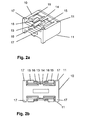
- FIG. 2a an isometric representation and the Fig. 2b a plan view of the blocking block.
- the blocking block 10 has a cuboidal basic shape and is designed as a hollow body. On both sides of its longitudinal sides 11 each two outwardly projecting, three-sided freestanding locking tabs 15 are formed, which are separated by a central strut 13.
- a partially wedge-shaped recess 16 is provided on each of the locking tabs 15, on both sides of the central strut 13.
- projections 17 are integrally formed on the four corner sides, which remain positioned when inserting a blocking block between two PCB connectors 3 above the horizontal longitudinal ribs 5, while the locking tabs 15 engage below the longitudinal ribs 5 in one of the window-like recesses 4. (See also Fig. 3 )
- part of the two locking lugs 15 adjoining the central strut 13 are wedge-shaped. Since the central strut 13 is withdrawn here, a Steckschlitz18, in which a corresponding tool, for. B. the tip of a screwdriver, can be used up to the level 14, so that each two adjacent locking tabs 15 bent back and the blocking block can be removed.
- the Fig. 3 shows a plan view of a plurality of parallel PCB connectors 3 between each of which a blocking block 10 has been used. It is in principle irrelevant at which of the four possible window-like recesses, a blocking block 10 is used to prevent the insertion of a particular version of the card stock.
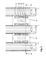
- Fig. 4 are in a sectional view of several of the Fig. 3 side by side spaced and arranged on a motherboard 1 printed circuit board connector 3 is shown, wherein between the connectors blocking blocks 10 are inserted.
- the daughter boards 2 can be designed for direct connection as a card edge connector or are combined in a multi-board plug-in attachment 22.
- the plug-in unit 20 shown here three daughter boards 2 are combined, which are provided for direct plugging into the printed circuit board connectors 3, the middle daughter board having a recess 24.
- This plug-in unit can be inserted easily, since the blocking block 10 fits exactly into the recess 24 of the middle daughter board. It is ensured in this plug-in unit that the middle daughter board forwards their signals through the two limiting circuit boards.
Landscapes
- Details Of Connecting Devices For Male And Female Coupling (AREA)
- Coupling Device And Connection With Printed Circuit (AREA)
- Combinations Of Printed Boards (AREA)
Abstract
Description
- Die Erfindung betrifft eine Blockiervorrichtung gegen Fehlsteckungen von Tochterleiterplatten auf einer Mutterleiterplatte, insbesondere, wenn mehrere Tochterleiterplatten zu einer Steckeinheit zusammengefasst sind und auf der Mutterleiterplatte mindestens zwei Leiterplattensteckverbinder kontaktieren.
- Eine derartige Vorrichtung wird benötigt, um zu verhindern, dass auf einer Mutterleiterplatte, die mit einer großen Anzahl von gleichartigen Leiterplattensteckverbindern besetzt ist, eine oder mehrere Tochterleiterplatten die wiederum zu einer Steckeinheit zusammengefasst sind, nicht in Bereiche auf der Mutterleiterplatte gesteckt wird, die für diese Konfiguration nicht vorgesehen sind und dabei eventuell Systemausfälle verursachen.
- Bei umfangreichen Backplanesystemen - also großen Mutterleiterplatten - mit gleichartigen Leiterplattensteckverbindern, die einem MicroTCA-System zugeordnet sind, können zwei verschiedene Arten von Modulsteckverbindern gesteckt werden. Das eine System ist unter dem Namen "Advanced Mezzanine Card" (AMCs) bekannt, während eine weiteres unter "Mezzanines with Auxiliary Connections" (Multitongue-AMCs) bekannt ist, das auch MicroTCA-Carrier-Hub-Module aufnimmt (MCH).
- Die Multitongue-AMC - Module sind Kartenrandsteckverbinder mit angefügten Leiterplatten, bei denen auf der Leiterkarte eine derartig große Anzahl von Signalkontakten vorgesehen ist, so dass zur Weiterleitung der Signale mindestens zwei separate Steckbereiche auf der Mutterleiterplatte notwendig sind.
- Werden darüber hinaus zwei Tochterleiterplatten zusammengefasst, so können drei oder vier Steckbereiche erforderlich sein, die über eine gleiche Anzahl von Leiterplattensteckverbindern ihre Signale auf die Backplane übertragen.
- Dabei können die zusammengefassten Tochterleiterplatten als Kartenrandstecker über deren Leiterbahnenenden direkt gesteckt werden oder mittels eines so genannten Mehrfach-Leiterplatten-Steckaufsatzes in die Leiterplattensteckverbinder auf der Mutterleiterplatte gesteckt werden.
- Dieser Mehrfach-Leiterplatten-Steckaufsatz wird separat gefertigt, mit den Leiterplatten verbunden und kontaktiert die Leiterplattensteckverbinder auf der Backplane.
- Da die Leiterplattensteckverbinder auf der Mutterleiterplatte für die AMCs und die Multitongue-AMCs jedoch die gleichen sind, aber eine unterschiedliche Kontaktbelegung aufweisen, muss sichergestellt werden, dass Fehlsteckungen bzw. Steckungen in nicht zulässigen Leiterplattensteckerbereichen vermieden werden.
- Der Erfindung liegt daher die Aufgabe zugrunde, dass eine aus mehreren Tochterleiterplatten bestehende Steckeinheit nicht in Bereiche auf der Mutterleiterplatte steckbar sind, die für diese Steckeinheit nicht vorgesehen sind.
- Diese Aufgabe wird dadurch gelöst, dass zwischen zwei in einem regulären Steckabstand angeordneten Leiterplattensteckverbindern ein Blockierblock eingefügt ist, dass an dem Blockierblock Rastlaschen vorgesehen sind, dass die Leiterplattensteckverbinder auf ihren Längsseiten fensterartige Ausnehmungen aufweisen, in denen die Rastlaschen des Blockierblockes einrasten, wobei der Blockierblock eine Steckung der als Steckeinheit zusammengefassten Tochterleiterplatten auf der Mutterleiterplatte verhindert.
- Eine vorteilhafte Ausgestaltung der Erfindung ist in den Ansprüchen 2-6 angegeben.
- Für die Übertragung einer großen Anzahl von Signalen von einer oder mehrerer Tochterleiterplatten steckbar auf eine Mutterleiterplatte, sind prinzipiell zwei Kontaktierungsmöglichkeiten vorgegeben, einmal eine direkte Steckung der Leiterbahnenden der Tochterleiterplatte in einen Leiterplattensteckverbinder auf der Mutterleiterplatte, und eine Steckung unter Inanspruchnahme eines zusätzlichen Steckverbinders, der mit der Tochterleiterplatte fest verbunden ist und dann in den Leiterplattensteckverbinder gesteckt wird.
- Wenn die Anzahl der nebeneinander oder in Sandwichkarten übereinander angeordneten Signalkontakte nicht mehr von einem Steckverbinder übertragen werden kann, wird ein Verbund mehrerer gestaffelter Steckverbinder, hier als Mehrfach-Leiterplatten-Steckaufsatz bezeichnet, genutzt.
- Da bei vielen Anwendungsfällen auf größeren Mutterleiterplatten auch gleichartige Leiterplattensteckverbinder eine unterschiedliche Kontaktbelegung aufweisen, besteht die Gefahr, dass Tochterleiterplatten an einem falschen Steckplatz gesteckt, zu kompletten Systemausfällen führen können.
- Zu einer Blockierung derartiger Steckbereiche ist vorgesehen, in die Zwischenräume des regulären Steckabstandes der Leiterplattensteckverbinder, ein Blockierelement einzufügen, das eine Fehlsteckung der Tochterleiterplatten-Steckeinheit verhindert.
- Dazu sind vorteilhafterweise die Leiterplattensteckverbinder auf der Backplane oder Mutterleiterplatte an ihren Längsseiten mit fensterartigen Ausnehmungen versehen, die durch Längsrippen und diese kreuzende Querrippen gebildet werden.
- Weiterhin weisen die vorgesehenen Blockierelemente vorteilhafterweise flexible Rastlaschen auf, die beim Einfügen zwischen zwei Leiterplattensteckverbindern an den Längsrippen verrasten und damit ein Stecken der Steckeinheit mit den verhindern.
- Vorsehbar sind dabei unterschiedliche Größen für die Kodierblöcke, die auch zwischen unterschiedlich voneinander entfernten angeordneten Leiterplattensteckverbinder eingefügbar sind.
- Ein Ausführungsbeispiel der Erfindung ist in der Zeichnung dargestellt und wird im folgenden näher erläutert. Es zeigen:
- Fig. 1
- einen Leiterplattensteckverbinder,
- Fig. 2a
- eine isometrische Darstellung eines Blockierblockes,
- Fig. 2b
- eine Draufsicht auf den Blockierblock,
- Fig. 3
- eine Draufsicht auf mehrere Leiterplattensteckverbinder mit dazwischen angeordneten Blockierblöcken,
- Fig. 4
- eine Schnittansicht aus der
Fig. 3 , und - Fig. 5
- die Kodierung einer Steckeinheit mittels des Blockierblockes.
- Die
Fig. 1 . zeigt eine Seitenansicht eines Leiterplattensteckverbinders 3 auf seine Längsseite, wobei hier vier fensterartige Ausnehmungen 4 erkennbar sind. - Die fensterartigen Ausnehmungen 4 sind als Vertiefungen ausgebildet, die durch mehrere senkrechte Querrippen 6 und sie kreuzende waagrechte Längsrippen 5 geformt sind.
- In den
Fig. 2a, 2b ist ein erfindungsgemäßer Blockierblock dargestellt. - Dabei zeigt die
Fig. 2a eine isometrische Darstellung und dieFig. 2b eine Draufsicht des Blockierblockes. - Der Blockierblock 10 weist eine quaderförmige Grundform auf und ist als Hohlkörper ausgeführt. Beidseitig seiner Längsseiten 11 sind jeweils zwei nach außen abstehende, dreiseitig freistehende Rastlaschen 15 ausgebildet, die durch eine mittige Strebe 13 getrennt sind.
- Weiterhin ist an jeder der Rastlaschen 15, beidseitig der mittigen Strebe 13, eine teilweise keilförmige Ausnehmung 16 vorgesehen.
- In diesem Bereich ist die mittige Strebe 13 um eine Stufe 14 gegenüber dem übrigen Niveau der Längsseite 11 zurückgenommen.
- Weiterhin sind an den vier Eckseiten Vorsprünge 17 angeformt, die beim Einfügen eines Blockierblockes zwischen zwei Leiterplattensteckverbinder 3 oberhalb der waagrechten Längsrippen 5 positioniert bleiben, während die Rastlaschen 15 unterhalb der Längsrippen 5 in einer der fensterartigen Ausnehmungen 4 verrasten. (Siehe dazu auch
Fig. 3 ) - Um einen verrasteten Blockierblock wieder entfernen zu können, ist ein Teil der beiden an die mittige Strebe 13 angrenzenden Rastlaschen 15 keilförmig ausgenommen. Da die mittige Strebe 13 hier zurückgenommen ist, entsteht ein Steckschlitz18, in den ein entsprechendes Werkzeug, z. B. die Spitze eines Schraubendrehers, bis zu der Stufe 14 eingesetzt werden kann, so dass jeweils zwei benachbarte Rastlaschen 15 zurückgebogen und der Blockierblock entfernt werden kann.
- Die
Fig. 3 zeigt eine Draufsicht auf mehrere parallel angeordnete Leiterplattensteckverbinder 3 zwischen denen jeweils ein Blockierblock 10 eingesetzt wurde. Dabei ist es prinzipiell unerheblich, an welcher der vier möglichen fensterartigen Ausnehmungen ein Blockierblock 10 eingesetzt wird, um die Steckung einer bestimmten Steckkartenversion zu unterbinden. - In der
Fig. 4 sind in einer Schnittansicht mehrere der aus derFig. 3 nebeneinander beabstandete und auf einer Mutterleiterplatte 1 angeordnete Leiterplattensteckverbinder 3 dargestellt, wobei zwischen den Steckverbindern Blockierblöcke 10 eingefügt sind. - Dabei ist deutlich erkennbar, wie die Enden der Rastlaschen 15 an den waagrechten Längsrippen 5 verrastet sind.
- Hieraus wird ersichtlich, wie ein eingefügter Blockierblock 10 die Steckung eine mehrere Tochterleiterplatten umfassende Steckeinheit 20 wirksam verhindert.
- Wobei die Tochterleiterplatten 2 zur direkten Steckung als Kartenrandstecker ausgeführt sein können oder in einem Mehrfach-Leiterplatten-Steckaufsatz 22 zusammengeführt sind.
- Eine einzelne Tochterleiterplatte kann hier natürlich problemlos gesteckt werden.
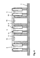
- Mittels der in den Leiterplattensteckverbindern 3 eingeformten Fenster 4 und mindestens einem Blockierblock 10 ist jedoch auch eine Kodierung einer Steckeinheit 20 möglich, wie dies in der
Fig. 5 dargestellt ist. - Dabei sind bei der hier gezeigten Steckeinheit 20 drei Tochterleiterplatten 2 zusammengefasst, die für eine direkte Steckung in die Leiterplattensteckverbinder 3 vorgesehen sind, wobei die mittlere Tochterleiterplatte eine Ausnehmung 24 aufweist.
- Auf der skizzierten Mutterleiterplatte 1 sind zwei Leiterplattensteckverbinder 3 und ein zwischen diesen verrasteter Blockierblock 10 angeordnet.
- Diese Steckeinheit kann problemlos gesteckt werden, da der Blockierblock 10 exakt in die Ausnehmung 24 der mittleren Tochterleiterplatte hineinpasst. Dabei ist bei dieser Steckeinheit sichergestellt, dass die mittlere Tochterleiterplatte ihre Signale über die beiden begrenzenden Leiterplatten weiterleitet.
- Somit kann nur diese eine Steckeinheit gesteckt werden - trotz der eigentlich blockierenden Aufgabe des Blockierblockes, die gegeben wäre, wenn die mittlere Tochterleiterplatte keine Ausnehmung aufweisen würde.
Claims (6)
- Blockiervorrichtung gegen Fehlsteckungen von Tochterleiterplatten (2) auf einer Mutterleiterplatte (1), insbesondere, wenn mehrere Tochterleiterplatten (2) zu einer Steckeinheit (20) zusammengefasst sind und auf der Mutterleiterplatte (1) mindestens zwei Leiterplattensteckverbinder (3) kontaktieren, dadurch gekennzeichnet,
dass zwischen zwei in einem regulären Steckabstand angeordneten Leiterplattensteckverbindern (3) ein Blockierblock (10) eingefügt ist, dass an dem Blockierblock (10) Rastlaschen (15) vorgesehen sind, dass die Leiterplattensteckverbinder (3) auf ihren Längsseiten fensterartige Ausnehmungen (4) aufweisen, in denen die Rastlaschen (15) des Blockierblockes (10) einrasten, wobei der Blockierblock (10) eine Steckung der als Steckeinheit (20) zusammengefassten Tochterleiterplatten (2) auf der Mutterleiterplatte (1) verhindert. - Blockiervorrichtung nach Anspruch 1, dadurch gekennzeichnet,
dass die fensterartigen Ausnehmungen (4) auf den Längsseiten der Leiterplattensteckverbinder (3) mittels Längsrippen (5) und sie kreuzende Querrippen (6) gebildet werden. - Blockiervorrichtung nach Anspruch 1, dadurch gekennzeichnet,
dass die Rastlaschen (15) des Blockierblockes (10) bereichsweise eine keilförmige Ausnehmung (16) aufweisen. - Blockiervorrichtung nach Anspruch 1, dadurch gekennzeichnet,
dass zwischen den Rastlaschen (15) eine mittlere Strebe (13) mit einer Stufe (14) vorgesehen ist. - Blockiervorrichtung nach Anspruch 1, dadurch gekennzeichnet,
dass ein verrasteter Blockierblock (10) mittels eines flachen Werkzeuges, welches in die keilförmigen Ausnehmungen (16) der beiden Rastlaschen (15) eingefügt wird, durch ein Zurückbiegen der Rastlaschen entgegen den Längsrippen (5) der Leiterplattensteckverbinder (3) entriegelbar ist. - Blockiervorrichtung nach Anspruch 1, dadurch gekennzeichnet,
dass der Blockierblock (10) in Zusammenhang mit einer oder mehreren Ausnehmungen (24) an der Steckseite an mindestens einer der Tochterleiterplatten (2) einer Steckeinheit (20) zu deren Kodierung vorgesehen ist.
Priority Applications (1)
| Application Number | Priority Date | Filing Date | Title |
|---|---|---|---|
| PL07023314T PL1930992T3 (pl) | 2006-12-08 | 2007-12-01 | Urządzenie blokujące błędne wetknięcia w złączach wtykowych płytek obwodu drukowanego |
Applications Claiming Priority (1)
| Application Number | Priority Date | Filing Date | Title |
|---|---|---|---|
| DE202006018590U DE202006018590U1 (de) | 2006-12-08 | 2006-12-08 | Blockiervorrichtung gegen Fehlsteckungen bei Leiterplattensteckverbindern |
Publications (3)
| Publication Number | Publication Date |
|---|---|
| EP1930992A2 true EP1930992A2 (de) | 2008-06-11 |
| EP1930992A3 EP1930992A3 (de) | 2009-12-16 |
| EP1930992B1 EP1930992B1 (de) | 2011-10-05 |
Family
ID=37776369
Family Applications (1)
| Application Number | Title | Priority Date | Filing Date |
|---|---|---|---|
| EP07023314A Active EP1930992B1 (de) | 2006-12-08 | 2007-12-01 | Blockiervorrichtung gegen Fehlsteckungen bei Leiterplattensteckverbindern |
Country Status (9)
| Country | Link |
|---|---|
| US (1) | US7503766B2 (de) |
| EP (1) | EP1930992B1 (de) |
| JP (1) | JP4700674B2 (de) |
| CN (1) | CN101197477B (de) |
| AT (1) | ATE527724T1 (de) |
| DE (1) | DE202006018590U1 (de) |
| DK (1) | DK1930992T3 (de) |
| ES (1) | ES2372764T3 (de) |
| PL (1) | PL1930992T3 (de) |
Families Citing this family (7)
| Publication number | Priority date | Publication date | Assignee | Title |
|---|---|---|---|---|
| FR3004859B1 (fr) * | 2013-04-19 | 2016-12-09 | Hypertac Sa | Connecteur electrique pour connecter une carte fille a une carte mere. |
| DE102013108888A1 (de) * | 2013-08-16 | 2015-02-19 | Phoenix Contact Gmbh & Co. Kg | Kodierung für Grundleisten mit einer Mehrzahl an Kammern |
| DE102014117233B4 (de) | 2014-11-25 | 2018-03-01 | Phoenix Contact Gmbh & Co. Kg | Grundleiste zum Verbinden mit einer Leiterplatte |
| US9609779B1 (en) * | 2015-02-03 | 2017-03-28 | Rick Sheffield | Apparatus for securing printed circuit boards |
| DE102015111972A1 (de) * | 2015-07-23 | 2017-01-26 | Abb Schweiz Ag | Schaltung auf Platinen in mehreren Ebenen mit Schnittstelle für Steckkarte |
| CN108566756B (zh) * | 2017-12-30 | 2024-04-26 | 河南思维轨道交通技术研究院有限公司 | 一种无线扎连接结构 |
| CN117222169B (zh) * | 2023-11-07 | 2024-03-08 | 江苏华鲲振宇智能科技有限责任公司 | 一种服务器双电源防误插拔互锁结构 |
Family Cites Families (9)
| Publication number | Priority date | Publication date | Assignee | Title |
|---|---|---|---|---|
| US3533045A (en) * | 1968-05-29 | 1970-10-06 | Amp Inc | Supporting and keying means for printed circuit boards or the like |
| DE2119709C3 (de) * | 1971-04-22 | 1986-02-13 | Siemens AG, 1000 Berlin und 8000 München | Baugruppenträger zur Aufnahme einschiebbarer elektrischer Baugruppen |
| US4046452A (en) * | 1975-04-16 | 1977-09-06 | Amp Incorporated | Electrical connector housing having an improved locking means |
| JPS555475U (de) * | 1978-06-26 | 1980-01-14 | ||
| JPH0299583U (de) * | 1989-01-27 | 1990-08-08 | ||
| US5014163A (en) * | 1990-01-30 | 1991-05-07 | John Lin | Structure of circuit board assembly |
| US6385053B1 (en) * | 1999-02-26 | 2002-05-07 | Cisco Technology, Inc. | PCB vertical and horizontal guide |
| JP2002298953A (ja) * | 2001-03-30 | 2002-10-11 | Nec Corp | コネクタ |
| JP4223525B2 (ja) * | 2005-10-27 | 2009-02-12 | 山一電機株式会社 | プラグコネクタ |
-
2006
- 2006-12-08 DE DE202006018590U patent/DE202006018590U1/de not_active Expired - Lifetime
-
2007
- 2007-11-27 US US11/945,863 patent/US7503766B2/en active Active
- 2007-12-01 ES ES07023314T patent/ES2372764T3/es active Active
- 2007-12-01 PL PL07023314T patent/PL1930992T3/pl unknown
- 2007-12-01 AT AT07023314T patent/ATE527724T1/de active
- 2007-12-01 DK DK07023314.3T patent/DK1930992T3/da active
- 2007-12-01 EP EP07023314A patent/EP1930992B1/de active Active
- 2007-12-06 JP JP2007316168A patent/JP4700674B2/ja not_active Expired - Fee Related
- 2007-12-07 CN CN2007101989181A patent/CN101197477B/zh active Active
Also Published As
| Publication number | Publication date |
|---|---|
| US7503766B2 (en) | 2009-03-17 |
| EP1930992A3 (de) | 2009-12-16 |
| CN101197477B (zh) | 2010-09-29 |
| DE202006018590U1 (de) | 2007-02-15 |
| US20080139010A1 (en) | 2008-06-12 |
| ATE527724T1 (de) | 2011-10-15 |
| ES2372764T3 (es) | 2012-01-26 |
| JP2008147192A (ja) | 2008-06-26 |
| CN101197477A (zh) | 2008-06-11 |
| PL1930992T3 (pl) | 2012-03-30 |
| JP4700674B2 (ja) | 2011-06-15 |
| EP1930992B1 (de) | 2011-10-05 |
| DK1930992T3 (da) | 2012-01-23 |
Similar Documents
| Publication | Publication Date | Title |
|---|---|---|
| DE69327132T2 (de) | Schalt-Zwischenebene und Zwischenverbindungssystem zum Untereinanderverbinden einer grossen Anzahl von Signalen | |
| EP2068228B1 (de) | Datenverarbeitungssystem | |
| EP1930992B1 (de) | Blockiervorrichtung gegen Fehlsteckungen bei Leiterplattensteckverbindern | |
| DE10036934A1 (de) | Hauptplatine | |
| DE102020123188A1 (de) | Modularer Steckverbinder zum Kontaktieren eines Gegensteckverbinders, insbesondere eines Leiterplattensteckverbinders | |
| EP1780837A2 (de) | Elektrische Anschlusseinrichtung für eine Leiterplatte | |
| DE9304928U1 (de) | Schirmeinrichtung für Kabelstecker | |
| DE10333913A1 (de) | Aderanschlussmodul für Leiterplatten | |
| DE10109571A1 (de) | Leiterplattenanordnung | |
| DE102011001486A1 (de) | Leiterplatten-Direktverbinder und Leiterplattenanordnung | |
| DE202010017834U1 (de) | Leiterplattenverbund | |
| DE9304929U1 (de) | Schirmeinrichtung für rechteckige Kabelstecker | |
| EP3066723B1 (de) | Prüfkabel sowie buchsenadapter für ein prüfkabel | |
| DE102021117571A1 (de) | Kraftfahrzeugsteuergerät | |
| DE102005059990A1 (de) | Steckverbinder zur Verbindung elektronischer Bauelemente | |
| DE3442056A1 (de) | Steckverbindervorrichtung | |
| DE102012204069B4 (de) | Elektrische Steckerverbindung | |
| WO2020114557A1 (de) | Adaptergehäuse für einen kontakteinsatz zur fixierung auf einer hutschiene | |
| EP1208727B1 (de) | Vorrichtung und brückenkarte für einen computer | |
| DE19526330C2 (de) | Vorrichtung zur Herstellung einer elektrischen und/oder optischen Verbindung | |
| DE202024101274U1 (de) | Zum Befestigen auf einer Befestigungsschiene eingerichtetes Modul | |
| DE102004031949A1 (de) | Elektrischer Steckverbinder | |
| DE102010040542B4 (de) | Überbrückungsbaustein und Verfahren mit einem Überbrückungsbaustein | |
| DE102011011995A1 (de) | Elektronikgerät, aufgebaut aus mindestens zwei Funktionsmodulen | |
| DE9315592U1 (de) | Computerbaugruppe |
Legal Events
| Date | Code | Title | Description |
|---|---|---|---|
| PUAI | Public reference made under article 153(3) epc to a published international application that has entered the european phase |
Free format text: ORIGINAL CODE: 0009012 |
|
| AK | Designated contracting states |
Kind code of ref document: A2 Designated state(s): AT BE BG CH CY CZ DE DK EE ES FI FR GB GR HU IE IS IT LI LT LU LV MC MT NL PL PT RO SE SI SK TR |
|
| AX | Request for extension of the european patent |
Extension state: AL BA HR MK RS |
|
| PUAL | Search report despatched |
Free format text: ORIGINAL CODE: 0009013 |
|
| AK | Designated contracting states |
Kind code of ref document: A3 Designated state(s): AT BE BG CH CY CZ DE DK EE ES FI FR GB GR HU IE IS IT LI LT LU LV MC MT NL PL PT RO SE SI SK TR |
|
| AX | Request for extension of the european patent |
Extension state: AL BA HR MK RS |
|
| 17P | Request for examination filed |
Effective date: 20100301 |
|
| AKX | Designation fees paid |
Designated state(s): AT BE BG CH CY CZ DE DK EE ES FI FR GB GR HU IE IS IT LI LT LU LV MC MT NL PL PT RO SE SI SK TR |
|
| REG | Reference to a national code |
Ref country code: DE Ref legal event code: R079 Ref document number: 502007008286 Country of ref document: DE Free format text: PREVIOUS MAIN CLASS: H01R0013640000 Ipc: H01R0012730000 |
|
| GRAP | Despatch of communication of intention to grant a patent |
Free format text: ORIGINAL CODE: EPIDOSNIGR1 |
|
| RIC1 | Information provided on ipc code assigned before grant |
Ipc: H01R 12/73 20110101AFI20110420BHEP Ipc: H01R 13/64 20060101ALI20110420BHEP |
|
| GRAS | Grant fee paid |
Free format text: ORIGINAL CODE: EPIDOSNIGR3 |
|
| GRAA | (expected) grant |
Free format text: ORIGINAL CODE: 0009210 |
|
| AK | Designated contracting states |
Kind code of ref document: B1 Designated state(s): AT BE BG CH CY CZ DE DK EE ES FI FR GB GR HU IE IS IT LI LT LU LV MC MT NL PL PT RO SE SI SK TR |
|
| REG | Reference to a national code |
Ref country code: GB Ref legal event code: FG4D Free format text: NOT ENGLISH |
|
| REG | Reference to a national code |
Ref country code: CH Ref legal event code: EP |
|
| REG | Reference to a national code |
Ref country code: IE Ref legal event code: FG4D |
|
| REG | Reference to a national code |
Ref country code: DE Ref legal event code: R096 Ref document number: 502007008286 Country of ref document: DE Effective date: 20111208 |
|
| REG | Reference to a national code |
Ref country code: RO Ref legal event code: EPE |
|
| REG | Reference to a national code |
Ref country code: SE Ref legal event code: TRGR |
|
| REG | Reference to a national code |
Ref country code: NL Ref legal event code: T3 |
|
| REG | Reference to a national code |
Ref country code: DK Ref legal event code: T3 |
|
| REG | Reference to a national code |
Ref country code: ES Ref legal event code: FG2A Ref document number: 2372764 Country of ref document: ES Kind code of ref document: T3 Effective date: 20120126 |
|
| PG25 | Lapsed in a contracting state [announced via postgrant information from national office to epo] |
Ref country code: SI Free format text: LAPSE BECAUSE OF FAILURE TO SUBMIT A TRANSLATION OF THE DESCRIPTION OR TO PAY THE FEE WITHIN THE PRESCRIBED TIME-LIMIT Effective date: 20111005 |
|
| LTIE | Lt: invalidation of european patent or patent extension |
Effective date: 20111005 |
|
| REG | Reference to a national code |
Ref country code: PL Ref legal event code: T3 |
|
| PG25 | Lapsed in a contracting state [announced via postgrant information from national office to epo] |
Ref country code: IS Free format text: LAPSE BECAUSE OF FAILURE TO SUBMIT A TRANSLATION OF THE DESCRIPTION OR TO PAY THE FEE WITHIN THE PRESCRIBED TIME-LIMIT Effective date: 20120205 Ref country code: LT Free format text: LAPSE BECAUSE OF FAILURE TO SUBMIT A TRANSLATION OF THE DESCRIPTION OR TO PAY THE FEE WITHIN THE PRESCRIBED TIME-LIMIT Effective date: 20111005 |
|
| REG | Reference to a national code |
Ref country code: IE Ref legal event code: FD4D |
|
| PG25 | Lapsed in a contracting state [announced via postgrant information from national office to epo] |
Ref country code: LV Free format text: LAPSE BECAUSE OF FAILURE TO SUBMIT A TRANSLATION OF THE DESCRIPTION OR TO PAY THE FEE WITHIN THE PRESCRIBED TIME-LIMIT Effective date: 20111005 Ref country code: GR Free format text: LAPSE BECAUSE OF FAILURE TO SUBMIT A TRANSLATION OF THE DESCRIPTION OR TO PAY THE FEE WITHIN THE PRESCRIBED TIME-LIMIT Effective date: 20120106 Ref country code: PT Free format text: LAPSE BECAUSE OF FAILURE TO SUBMIT A TRANSLATION OF THE DESCRIPTION OR TO PAY THE FEE WITHIN THE PRESCRIBED TIME-LIMIT Effective date: 20120206 |
|
| PG25 | Lapsed in a contracting state [announced via postgrant information from national office to epo] |
Ref country code: CY Free format text: LAPSE BECAUSE OF FAILURE TO SUBMIT A TRANSLATION OF THE DESCRIPTION OR TO PAY THE FEE WITHIN THE PRESCRIBED TIME-LIMIT Effective date: 20111005 |
|
| PG25 | Lapsed in a contracting state [announced via postgrant information from national office to epo] |
Ref country code: MC Free format text: LAPSE BECAUSE OF NON-PAYMENT OF DUE FEES Effective date: 20111231 Ref country code: SK Free format text: LAPSE BECAUSE OF FAILURE TO SUBMIT A TRANSLATION OF THE DESCRIPTION OR TO PAY THE FEE WITHIN THE PRESCRIBED TIME-LIMIT Effective date: 20111005 Ref country code: BG Free format text: LAPSE BECAUSE OF FAILURE TO SUBMIT A TRANSLATION OF THE DESCRIPTION OR TO PAY THE FEE WITHIN THE PRESCRIBED TIME-LIMIT Effective date: 20120105 Ref country code: EE Free format text: LAPSE BECAUSE OF FAILURE TO SUBMIT A TRANSLATION OF THE DESCRIPTION OR TO PAY THE FEE WITHIN THE PRESCRIBED TIME-LIMIT Effective date: 20111005 Ref country code: IE Free format text: LAPSE BECAUSE OF FAILURE TO SUBMIT A TRANSLATION OF THE DESCRIPTION OR TO PAY THE FEE WITHIN THE PRESCRIBED TIME-LIMIT Effective date: 20111005 |
|
| PLBE | No opposition filed within time limit |
Free format text: ORIGINAL CODE: 0009261 |
|
| STAA | Information on the status of an ep patent application or granted ep patent |
Free format text: STATUS: NO OPPOSITION FILED WITHIN TIME LIMIT |
|
| 26N | No opposition filed |
Effective date: 20120706 |
|
| REG | Reference to a national code |
Ref country code: DE Ref legal event code: R097 Ref document number: 502007008286 Country of ref document: DE Effective date: 20120706 |
|
| PG25 | Lapsed in a contracting state [announced via postgrant information from national office to epo] |
Ref country code: MT Free format text: LAPSE BECAUSE OF FAILURE TO SUBMIT A TRANSLATION OF THE DESCRIPTION OR TO PAY THE FEE WITHIN THE PRESCRIBED TIME-LIMIT Effective date: 20111005 |
|
| PG25 | Lapsed in a contracting state [announced via postgrant information from national office to epo] |
Ref country code: LU Free format text: LAPSE BECAUSE OF NON-PAYMENT OF DUE FEES Effective date: 20111201 |
|
| PG25 | Lapsed in a contracting state [announced via postgrant information from national office to epo] |
Ref country code: HU Free format text: LAPSE BECAUSE OF FAILURE TO SUBMIT A TRANSLATION OF THE DESCRIPTION OR TO PAY THE FEE WITHIN THE PRESCRIBED TIME-LIMIT Effective date: 20111005 |
|
| REG | Reference to a national code |
Ref country code: FR Ref legal event code: PLFP Year of fee payment: 9 |
|
| PGFP | Annual fee paid to national office [announced via postgrant information from national office to epo] |
Ref country code: TR Payment date: 20151022 Year of fee payment: 9 Ref country code: CH Payment date: 20151211 Year of fee payment: 9 Ref country code: FI Payment date: 20151209 Year of fee payment: 9 Ref country code: DK Payment date: 20151210 Year of fee payment: 9 |
|
| PGFP | Annual fee paid to national office [announced via postgrant information from national office to epo] |
Ref country code: NL Payment date: 20151210 Year of fee payment: 9 Ref country code: AT Payment date: 20151125 Year of fee payment: 9 Ref country code: BE Payment date: 20151207 Year of fee payment: 9 Ref country code: CZ Payment date: 20151116 Year of fee payment: 9 Ref country code: RO Payment date: 20151106 Year of fee payment: 9 Ref country code: PL Payment date: 20151013 Year of fee payment: 9 Ref country code: SE Payment date: 20151211 Year of fee payment: 9 Ref country code: ES Payment date: 20151111 Year of fee payment: 9 |
|
| PGFP | Annual fee paid to national office [announced via postgrant information from national office to epo] |
Ref country code: IT Payment date: 20151221 Year of fee payment: 9 |
|
| REG | Reference to a national code |
Ref country code: DE Ref legal event code: R081 Ref document number: 502007008286 Country of ref document: DE Owner name: HARTING ELECTRONICS GMBH, DE Free format text: FORMER OWNER: HARTING ELECTRONICS GMBH & CO. KG, 32339 ESPELKAMP, DE |
|
| REG | Reference to a national code |
Ref country code: FR Ref legal event code: PLFP Year of fee payment: 10 |
|
| PG25 | Lapsed in a contracting state [announced via postgrant information from national office to epo] |
Ref country code: BE Free format text: LAPSE BECAUSE OF NON-PAYMENT OF DUE FEES Effective date: 20161231 |
|
| PG25 | Lapsed in a contracting state [announced via postgrant information from national office to epo] |
Ref country code: CZ Free format text: LAPSE BECAUSE OF NON-PAYMENT OF DUE FEES Effective date: 20161201 Ref country code: RO Free format text: LAPSE BECAUSE OF NON-PAYMENT OF DUE FEES Effective date: 20161201 Ref country code: FI Free format text: LAPSE BECAUSE OF NON-PAYMENT OF DUE FEES Effective date: 20161201 |
|
| REG | Reference to a national code |
Ref country code: DK Ref legal event code: EBP Effective date: 20161231 Ref country code: CH Ref legal event code: PL |
|
| REG | Reference to a national code |
Ref country code: SE Ref legal event code: EUG |
|
| REG | Reference to a national code |
Ref country code: NL Ref legal event code: MM Effective date: 20170101 |
|
| REG | Reference to a national code |
Ref country code: AT Ref legal event code: MM01 Ref document number: 527724 Country of ref document: AT Kind code of ref document: T Effective date: 20161201 |
|
| PG25 | Lapsed in a contracting state [announced via postgrant information from national office to epo] |
Ref country code: SE Free format text: LAPSE BECAUSE OF NON-PAYMENT OF DUE FEES Effective date: 20161202 |
|
| PG25 | Lapsed in a contracting state [announced via postgrant information from national office to epo] |
Ref country code: NL Free format text: LAPSE BECAUSE OF NON-PAYMENT OF DUE FEES Effective date: 20170101 |
|
| PG25 | Lapsed in a contracting state [announced via postgrant information from national office to epo] |
Ref country code: CH Free format text: LAPSE BECAUSE OF NON-PAYMENT OF DUE FEES Effective date: 20161231 Ref country code: AT Free format text: LAPSE BECAUSE OF NON-PAYMENT OF DUE FEES Effective date: 20161201 Ref country code: LI Free format text: LAPSE BECAUSE OF NON-PAYMENT OF DUE FEES Effective date: 20161231 Ref country code: IT Free format text: LAPSE BECAUSE OF NON-PAYMENT OF DUE FEES Effective date: 20161201 |
|
| REG | Reference to a national code |
Ref country code: FR Ref legal event code: PLFP Year of fee payment: 11 |
|
| PG25 | Lapsed in a contracting state [announced via postgrant information from national office to epo] |
Ref country code: DK Free format text: LAPSE BECAUSE OF NON-PAYMENT OF DUE FEES Effective date: 20161231 |
|
| REG | Reference to a national code |
Ref country code: BE Ref legal event code: MM Effective date: 20161231 |
|
| PG25 | Lapsed in a contracting state [announced via postgrant information from national office to epo] |
Ref country code: PL Free format text: LAPSE BECAUSE OF NON-PAYMENT OF DUE FEES Effective date: 20161201 |
|
| PG25 | Lapsed in a contracting state [announced via postgrant information from national office to epo] |
Ref country code: ES Free format text: LAPSE BECAUSE OF NON-PAYMENT OF DUE FEES Effective date: 20161202 |
|
| REG | Reference to a national code |
Ref country code: ES Ref legal event code: FD2A Effective date: 20181120 |
|
| PG25 | Lapsed in a contracting state [announced via postgrant information from national office to epo] |
Ref country code: TR Free format text: LAPSE BECAUSE OF NON-PAYMENT OF DUE FEES Effective date: 20161201 |
|
| P01 | Opt-out of the competence of the unified patent court (upc) registered |
Effective date: 20230603 |
|
| PGFP | Annual fee paid to national office [announced via postgrant information from national office to epo] |
Ref country code: GB Payment date: 20251223 Year of fee payment: 19 |
|
| PGFP | Annual fee paid to national office [announced via postgrant information from national office to epo] |
Ref country code: FR Payment date: 20251223 Year of fee payment: 19 |
|
| PGFP | Annual fee paid to national office [announced via postgrant information from national office to epo] |
Ref country code: DE Payment date: 20251229 Year of fee payment: 19 |