EP1930992A2 - Dispositif de blocage contre les mauvais enfichages pour connecteurs enfichables de cartes de circuits imprimés - Google Patents
Dispositif de blocage contre les mauvais enfichages pour connecteurs enfichables de cartes de circuits imprimés Download PDFInfo
- Publication number
- EP1930992A2 EP1930992A2 EP07023314A EP07023314A EP1930992A2 EP 1930992 A2 EP1930992 A2 EP 1930992A2 EP 07023314 A EP07023314 A EP 07023314A EP 07023314 A EP07023314 A EP 07023314A EP 1930992 A2 EP1930992 A2 EP 1930992A2
- Authority
- EP
- European Patent Office
- Prior art keywords
- plug
- blocking block
- printed circuit
- circuit board
- blocking
- Prior art date
- Legal status (The legal status is an assumption and is not a legal conclusion. Google has not performed a legal analysis and makes no representation as to the accuracy of the status listed.)
- Granted
Links
Images


Classifications
-
- H—ELECTRICITY
- H01—ELECTRIC ELEMENTS
- H01R—ELECTRICALLY-CONDUCTIVE CONNECTIONS; STRUCTURAL ASSOCIATIONS OF A PLURALITY OF MUTUALLY-INSULATED ELECTRICAL CONNECTING ELEMENTS; COUPLING DEVICES; CURRENT COLLECTORS
- H01R13/00—Details of coupling devices of the kinds covered by groups H01R12/70 or H01R24/00 - H01R33/00
- H01R13/64—Means for preventing incorrect coupling
- H01R13/645—Means for preventing incorrect coupling by exchangeable elements on case or base
- H01R13/6456—Means for preventing incorrect coupling by exchangeable elements on case or base comprising keying elements at different positions along the periphery of the connector
-
- H—ELECTRICITY
- H01—ELECTRIC ELEMENTS
- H01R—ELECTRICALLY-CONDUCTIVE CONNECTIONS; STRUCTURAL ASSOCIATIONS OF A PLURALITY OF MUTUALLY-INSULATED ELECTRICAL CONNECTING ELEMENTS; COUPLING DEVICES; CURRENT COLLECTORS
- H01R12/00—Structural associations of a plurality of mutually-insulated electrical connecting elements, specially adapted for printed circuits, e.g. printed circuit boards [PCB], flat or ribbon cables, or like generally planar structures, e.g. terminal strips, terminal blocks; Coupling devices specially adapted for printed circuits, flat or ribbon cables, or like generally planar structures; Terminals specially adapted for contact with, or insertion into, printed circuits, flat or ribbon cables, or like generally planar structures
- H01R12/70—Coupling devices
- H01R12/7005—Guiding, mounting, polarizing or locking means; Extractors
-
- H—ELECTRICITY
- H01—ELECTRIC ELEMENTS
- H01R—ELECTRICALLY-CONDUCTIVE CONNECTIONS; STRUCTURAL ASSOCIATIONS OF A PLURALITY OF MUTUALLY-INSULATED ELECTRICAL CONNECTING ELEMENTS; COUPLING DEVICES; CURRENT COLLECTORS
- H01R12/00—Structural associations of a plurality of mutually-insulated electrical connecting elements, specially adapted for printed circuits, e.g. printed circuit boards [PCB], flat or ribbon cables, or like generally planar structures, e.g. terminal strips, terminal blocks; Coupling devices specially adapted for printed circuits, flat or ribbon cables, or like generally planar structures; Terminals specially adapted for contact with, or insertion into, printed circuits, flat or ribbon cables, or like generally planar structures
- H01R12/70—Coupling devices
- H01R12/71—Coupling devices for rigid printing circuits or like structures
- H01R12/712—Coupling devices for rigid printing circuits or like structures co-operating with the surface of the printed circuit or with a coupling device exclusively provided on the surface of the printed circuit
- H01R12/716—Coupling device provided on the PCB
-
- H—ELECTRICITY
- H01—ELECTRIC ELEMENTS
- H01R—ELECTRICALLY-CONDUCTIVE CONNECTIONS; STRUCTURAL ASSOCIATIONS OF A PLURALITY OF MUTUALLY-INSULATED ELECTRICAL CONNECTING ELEMENTS; COUPLING DEVICES; CURRENT COLLECTORS
- H01R12/00—Structural associations of a plurality of mutually-insulated electrical connecting elements, specially adapted for printed circuits, e.g. printed circuit boards [PCB], flat or ribbon cables, or like generally planar structures, e.g. terminal strips, terminal blocks; Coupling devices specially adapted for printed circuits, flat or ribbon cables, or like generally planar structures; Terminals specially adapted for contact with, or insertion into, printed circuits, flat or ribbon cables, or like generally planar structures
- H01R12/70—Coupling devices
- H01R12/7082—Coupling device supported only by cooperation with PCB
Definitions
- the invention relates to a blocking device against misinsertion of daughter boards on a motherboard, in particular, when a plurality of daughter boards are combined to form a plug-in unit and contact on the motherboard at least two PCB connectors.
- Such a device is needed to prevent one or more daughter boards, which in turn are assembled into a plug-in unit on a mother board occupied by a large number of similar board connectors, from being plugged into areas on the mother board that are for them Configuration are not provided and thereby possibly cause system failure.
- AMCs Advanced Mezzanine Card
- MCH MicroTCA Carrier Hub Modules
- the multitongue AMC modules are card edge connectors with attached printed circuit boards, in which on the circuit board such a large number of signal contacts is provided, so that for forwarding the signals at least two separate plug-in areas on the motherboard are necessary.
- the combined daughter boards can be plugged as a card edge connector on their conductor ends directly or plugged by means of a so-called multi-board plug-in attachment in the PCB connectors on the motherboard.
- This multi-board connector is manufactured separately, connected to the circuit boards and contacts the PCB connectors on the backplane.
- the invention is therefore based on the object that a plug-in unit consisting of several daughter boards are not pluggable into areas on the motherboard that are not provided for this plug-in unit.
- This object is achieved in that between two arranged in a regular spacing PCB connectors a blocking block is inserted, that locking tabs are provided on the blocking block that the PCB connectors on their longitudinal sides have window-like recesses in which engage the locking tabs of the blocking block, the blocking block a Plugging the summarized as plug-in daughter circuit boards on the mother board prevented.
- a composite of several staggered connector referred to here as a multi-circuit board connector, used.
- the printed circuit board connectors on the backplane or motherboard plate are advantageously provided on their longitudinal sides with window-like recesses, which are formed by longitudinal ribs and these crossing transverse ribs.
- the blocking elements provided advantageously have flexible locking tabs which latch when inserted between two PCB connectors to the longitudinal ribs and thus prevent plugging the plug-in unit with the.
- Predictable are different sizes for the coding blocks, which are also inserted between differently spaced apart PCB connectors.
- the Fig. 1 shows a side view of a printed circuit board connector 3 on its longitudinal side, in which case four window-like recesses 4 can be seen.
- the window-like recesses 4 are formed as depressions, which are formed by a plurality of vertical transverse ribs 6 and they crossing horizontal longitudinal ribs 5.
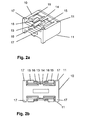
- FIG. 2a an isometric representation and the Fig. 2b a plan view of the blocking block.
- the blocking block 10 has a cuboidal basic shape and is designed as a hollow body. On both sides of its longitudinal sides 11 each two outwardly projecting, three-sided freestanding locking tabs 15 are formed, which are separated by a central strut 13.
- a partially wedge-shaped recess 16 is provided on each of the locking tabs 15, on both sides of the central strut 13.
- projections 17 are integrally formed on the four corner sides, which remain positioned when inserting a blocking block between two PCB connectors 3 above the horizontal longitudinal ribs 5, while the locking tabs 15 engage below the longitudinal ribs 5 in one of the window-like recesses 4. (See also Fig. 3 )
- part of the two locking lugs 15 adjoining the central strut 13 are wedge-shaped. Since the central strut 13 is withdrawn here, a Steckschlitz18, in which a corresponding tool, for. B. the tip of a screwdriver, can be used up to the level 14, so that each two adjacent locking tabs 15 bent back and the blocking block can be removed.
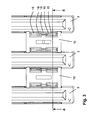
- the Fig. 3 shows a plan view of a plurality of parallel PCB connectors 3 between each of which a blocking block 10 has been used. It is in principle irrelevant at which of the four possible window-like recesses, a blocking block 10 is used to prevent the insertion of a particular version of the card stock.
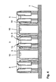
- Fig. 4 are in a sectional view of several of the Fig. 3 side by side spaced and arranged on a motherboard 1 printed circuit board connector 3 is shown, wherein between the connectors blocking blocks 10 are inserted.
- the daughter boards 2 can be designed for direct connection as a card edge connector or are combined in a multi-board plug-in attachment 22.
- the plug-in unit 20 shown here three daughter boards 2 are combined, which are provided for direct plugging into the printed circuit board connectors 3, the middle daughter board having a recess 24.
- This plug-in unit can be inserted easily, since the blocking block 10 fits exactly into the recess 24 of the middle daughter board. It is ensured in this plug-in unit that the middle daughter board forwards their signals through the two limiting circuit boards.
Landscapes
- Details Of Connecting Devices For Male And Female Coupling (AREA)
- Coupling Device And Connection With Printed Circuit (AREA)
- Combinations Of Printed Boards (AREA)
Priority Applications (1)
| Application Number | Priority Date | Filing Date | Title |
|---|---|---|---|
| PL07023314T PL1930992T3 (pl) | 2006-12-08 | 2007-12-01 | Urządzenie blokujące błędne wetknięcia w złączach wtykowych płytek obwodu drukowanego |
Applications Claiming Priority (1)
| Application Number | Priority Date | Filing Date | Title |
|---|---|---|---|
| DE202006018590U DE202006018590U1 (de) | 2006-12-08 | 2006-12-08 | Blockiervorrichtung gegen Fehlsteckungen bei Leiterplattensteckverbindern |
Publications (3)
| Publication Number | Publication Date |
|---|---|
| EP1930992A2 true EP1930992A2 (fr) | 2008-06-11 |
| EP1930992A3 EP1930992A3 (fr) | 2009-12-16 |
| EP1930992B1 EP1930992B1 (fr) | 2011-10-05 |
Family
ID=37776369
Family Applications (1)
| Application Number | Title | Priority Date | Filing Date |
|---|---|---|---|
| EP07023314A Active EP1930992B1 (fr) | 2006-12-08 | 2007-12-01 | Dispositif de blocage contre les mauvais enfichages pour connecteurs enfichables de cartes de circuits imprimés |
Country Status (9)
| Country | Link |
|---|---|
| US (1) | US7503766B2 (fr) |
| EP (1) | EP1930992B1 (fr) |
| JP (1) | JP4700674B2 (fr) |
| CN (1) | CN101197477B (fr) |
| AT (1) | ATE527724T1 (fr) |
| DE (1) | DE202006018590U1 (fr) |
| DK (1) | DK1930992T3 (fr) |
| ES (1) | ES2372764T3 (fr) |
| PL (1) | PL1930992T3 (fr) |
Families Citing this family (7)
| Publication number | Priority date | Publication date | Assignee | Title |
|---|---|---|---|---|
| FR3004859B1 (fr) * | 2013-04-19 | 2016-12-09 | Hypertac Sa | Connecteur electrique pour connecter une carte fille a une carte mere. |
| DE102013108888A1 (de) * | 2013-08-16 | 2015-02-19 | Phoenix Contact Gmbh & Co. Kg | Kodierung für Grundleisten mit einer Mehrzahl an Kammern |
| DE102014117233B4 (de) | 2014-11-25 | 2018-03-01 | Phoenix Contact Gmbh & Co. Kg | Grundleiste zum Verbinden mit einer Leiterplatte |
| US9609779B1 (en) * | 2015-02-03 | 2017-03-28 | Rick Sheffield | Apparatus for securing printed circuit boards |
| DE102015111972A1 (de) * | 2015-07-23 | 2017-01-26 | Abb Schweiz Ag | Schaltung auf Platinen in mehreren Ebenen mit Schnittstelle für Steckkarte |
| CN108566756B (zh) * | 2017-12-30 | 2024-04-26 | 河南思维轨道交通技术研究院有限公司 | 一种无线扎连接结构 |
| CN117222169B (zh) * | 2023-11-07 | 2024-03-08 | 江苏华鲲振宇智能科技有限责任公司 | 一种服务器双电源防误插拔互锁结构 |
Family Cites Families (9)
| Publication number | Priority date | Publication date | Assignee | Title |
|---|---|---|---|---|
| US3533045A (en) * | 1968-05-29 | 1970-10-06 | Amp Inc | Supporting and keying means for printed circuit boards or the like |
| DE2119709C3 (de) * | 1971-04-22 | 1986-02-13 | Siemens AG, 1000 Berlin und 8000 München | Baugruppenträger zur Aufnahme einschiebbarer elektrischer Baugruppen |
| US4046452A (en) * | 1975-04-16 | 1977-09-06 | Amp Incorporated | Electrical connector housing having an improved locking means |
| JPS555475U (fr) * | 1978-06-26 | 1980-01-14 | ||
| JPH0299583U (fr) * | 1989-01-27 | 1990-08-08 | ||
| US5014163A (en) * | 1990-01-30 | 1991-05-07 | John Lin | Structure of circuit board assembly |
| US6385053B1 (en) * | 1999-02-26 | 2002-05-07 | Cisco Technology, Inc. | PCB vertical and horizontal guide |
| JP2002298953A (ja) * | 2001-03-30 | 2002-10-11 | Nec Corp | コネクタ |
| JP4223525B2 (ja) * | 2005-10-27 | 2009-02-12 | 山一電機株式会社 | プラグコネクタ |
-
2006
- 2006-12-08 DE DE202006018590U patent/DE202006018590U1/de not_active Expired - Lifetime
-
2007
- 2007-11-27 US US11/945,863 patent/US7503766B2/en active Active
- 2007-12-01 ES ES07023314T patent/ES2372764T3/es active Active
- 2007-12-01 AT AT07023314T patent/ATE527724T1/de active
- 2007-12-01 DK DK07023314.3T patent/DK1930992T3/da active
- 2007-12-01 PL PL07023314T patent/PL1930992T3/pl unknown
- 2007-12-01 EP EP07023314A patent/EP1930992B1/fr active Active
- 2007-12-06 JP JP2007316168A patent/JP4700674B2/ja not_active Expired - Fee Related
- 2007-12-07 CN CN2007101989181A patent/CN101197477B/zh active Active
Also Published As
| Publication number | Publication date |
|---|---|
| PL1930992T3 (pl) | 2012-03-30 |
| ATE527724T1 (de) | 2011-10-15 |
| ES2372764T3 (es) | 2012-01-26 |
| EP1930992B1 (fr) | 2011-10-05 |
| US20080139010A1 (en) | 2008-06-12 |
| JP2008147192A (ja) | 2008-06-26 |
| EP1930992A3 (fr) | 2009-12-16 |
| DE202006018590U1 (de) | 2007-02-15 |
| CN101197477A (zh) | 2008-06-11 |
| DK1930992T3 (da) | 2012-01-23 |
| JP4700674B2 (ja) | 2011-06-15 |
| US7503766B2 (en) | 2009-03-17 |
| CN101197477B (zh) | 2010-09-29 |
Similar Documents
| Publication | Publication Date | Title |
|---|---|---|
| DE69327132T2 (de) | Schalt-Zwischenebene und Zwischenverbindungssystem zum Untereinanderverbinden einer grossen Anzahl von Signalen | |
| EP2068228B1 (fr) | Système de traitement des données | |
| EP1930992B1 (fr) | Dispositif de blocage contre les mauvais enfichages pour connecteurs enfichables de cartes de circuits imprimés | |
| DE10036934A1 (de) | Hauptplatine | |
| DE102020123188A1 (de) | Modularer Steckverbinder zum Kontaktieren eines Gegensteckverbinders, insbesondere eines Leiterplattensteckverbinders | |
| EP1780837A2 (fr) | Dispositif de raccordement électrique pour carte de circuit | |
| DE9304928U1 (de) | Schirmeinrichtung für Kabelstecker | |
| DE10333913A1 (de) | Aderanschlussmodul für Leiterplatten | |
| DE10109571A1 (de) | Leiterplattenanordnung | |
| DE102011001486A1 (de) | Leiterplatten-Direktverbinder und Leiterplattenanordnung | |
| DE202010017834U1 (de) | Leiterplattenverbund | |
| DE9304929U1 (de) | Schirmeinrichtung für rechteckige Kabelstecker | |
| EP3066723B1 (fr) | Câble d'essai ainsi qu'adaptateur de prise pour un câble d'essai | |
| DE102021117571A1 (de) | Kraftfahrzeugsteuergerät | |
| DE102005059990A1 (de) | Steckverbinder zur Verbindung elektronischer Bauelemente | |
| DE3442056A1 (de) | Steckverbindervorrichtung | |
| DE102012204069B4 (de) | Elektrische Steckerverbindung | |
| EP1208727B1 (fr) | Dispositif et carte en pont pour un ordinateur | |
| DE19526330C2 (de) | Vorrichtung zur Herstellung einer elektrischen und/oder optischen Verbindung | |
| DE202024101274U1 (de) | Zum Befestigen auf einer Befestigungsschiene eingerichtetes Modul | |
| DE102004031949A1 (de) | Elektrischer Steckverbinder | |
| DE102010040542B4 (de) | Überbrückungsbaustein und Verfahren mit einem Überbrückungsbaustein | |
| DE102011011995A1 (de) | Elektronikgerät, aufgebaut aus mindestens zwei Funktionsmodulen | |
| DE9315592U1 (de) | Computerbaugruppe | |
| WO2023202743A1 (fr) | Connecteur de bus pour un système de commande électrique |
Legal Events
| Date | Code | Title | Description |
|---|---|---|---|
| PUAI | Public reference made under article 153(3) epc to a published international application that has entered the european phase |
Free format text: ORIGINAL CODE: 0009012 |
|
| AK | Designated contracting states |
Kind code of ref document: A2 Designated state(s): AT BE BG CH CY CZ DE DK EE ES FI FR GB GR HU IE IS IT LI LT LU LV MC MT NL PL PT RO SE SI SK TR |
|
| AX | Request for extension of the european patent |
Extension state: AL BA HR MK RS |
|
| PUAL | Search report despatched |
Free format text: ORIGINAL CODE: 0009013 |
|
| AK | Designated contracting states |
Kind code of ref document: A3 Designated state(s): AT BE BG CH CY CZ DE DK EE ES FI FR GB GR HU IE IS IT LI LT LU LV MC MT NL PL PT RO SE SI SK TR |
|
| AX | Request for extension of the european patent |
Extension state: AL BA HR MK RS |
|
| 17P | Request for examination filed |
Effective date: 20100301 |
|
| AKX | Designation fees paid |
Designated state(s): AT BE BG CH CY CZ DE DK EE ES FI FR GB GR HU IE IS IT LI LT LU LV MC MT NL PL PT RO SE SI SK TR |
|
| REG | Reference to a national code |
Ref country code: DE Ref legal event code: R079 Ref document number: 502007008286 Country of ref document: DE Free format text: PREVIOUS MAIN CLASS: H01R0013640000 Ipc: H01R0012730000 |
|
| GRAP | Despatch of communication of intention to grant a patent |
Free format text: ORIGINAL CODE: EPIDOSNIGR1 |
|
| RIC1 | Information provided on ipc code assigned before grant |
Ipc: H01R 12/73 20110101AFI20110420BHEP Ipc: H01R 13/64 20060101ALI20110420BHEP |
|
| GRAS | Grant fee paid |
Free format text: ORIGINAL CODE: EPIDOSNIGR3 |
|
| GRAA | (expected) grant |
Free format text: ORIGINAL CODE: 0009210 |
|
| AK | Designated contracting states |
Kind code of ref document: B1 Designated state(s): AT BE BG CH CY CZ DE DK EE ES FI FR GB GR HU IE IS IT LI LT LU LV MC MT NL PL PT RO SE SI SK TR |
|
| REG | Reference to a national code |
Ref country code: GB Ref legal event code: FG4D Free format text: NOT ENGLISH |
|
| REG | Reference to a national code |
Ref country code: CH Ref legal event code: EP |
|
| REG | Reference to a national code |
Ref country code: IE Ref legal event code: FG4D |
|
| REG | Reference to a national code |
Ref country code: DE Ref legal event code: R096 Ref document number: 502007008286 Country of ref document: DE Effective date: 20111208 |
|
| REG | Reference to a national code |
Ref country code: RO Ref legal event code: EPE |
|
| REG | Reference to a national code |
Ref country code: SE Ref legal event code: TRGR |
|
| REG | Reference to a national code |
Ref country code: NL Ref legal event code: T3 |
|
| REG | Reference to a national code |
Ref country code: DK Ref legal event code: T3 |
|
| REG | Reference to a national code |
Ref country code: ES Ref legal event code: FG2A Ref document number: 2372764 Country of ref document: ES Kind code of ref document: T3 Effective date: 20120126 |
|
| PG25 | Lapsed in a contracting state [announced via postgrant information from national office to epo] |
Ref country code: SI Free format text: LAPSE BECAUSE OF FAILURE TO SUBMIT A TRANSLATION OF THE DESCRIPTION OR TO PAY THE FEE WITHIN THE PRESCRIBED TIME-LIMIT Effective date: 20111005 |
|
| LTIE | Lt: invalidation of european patent or patent extension |
Effective date: 20111005 |
|
| REG | Reference to a national code |
Ref country code: PL Ref legal event code: T3 |
|
| PG25 | Lapsed in a contracting state [announced via postgrant information from national office to epo] |
Ref country code: IS Free format text: LAPSE BECAUSE OF FAILURE TO SUBMIT A TRANSLATION OF THE DESCRIPTION OR TO PAY THE FEE WITHIN THE PRESCRIBED TIME-LIMIT Effective date: 20120205 Ref country code: LT Free format text: LAPSE BECAUSE OF FAILURE TO SUBMIT A TRANSLATION OF THE DESCRIPTION OR TO PAY THE FEE WITHIN THE PRESCRIBED TIME-LIMIT Effective date: 20111005 |
|
| REG | Reference to a national code |
Ref country code: IE Ref legal event code: FD4D |
|
| PG25 | Lapsed in a contracting state [announced via postgrant information from national office to epo] |
Ref country code: LV Free format text: LAPSE BECAUSE OF FAILURE TO SUBMIT A TRANSLATION OF THE DESCRIPTION OR TO PAY THE FEE WITHIN THE PRESCRIBED TIME-LIMIT Effective date: 20111005 Ref country code: GR Free format text: LAPSE BECAUSE OF FAILURE TO SUBMIT A TRANSLATION OF THE DESCRIPTION OR TO PAY THE FEE WITHIN THE PRESCRIBED TIME-LIMIT Effective date: 20120106 Ref country code: PT Free format text: LAPSE BECAUSE OF FAILURE TO SUBMIT A TRANSLATION OF THE DESCRIPTION OR TO PAY THE FEE WITHIN THE PRESCRIBED TIME-LIMIT Effective date: 20120206 |
|
| PG25 | Lapsed in a contracting state [announced via postgrant information from national office to epo] |
Ref country code: CY Free format text: LAPSE BECAUSE OF FAILURE TO SUBMIT A TRANSLATION OF THE DESCRIPTION OR TO PAY THE FEE WITHIN THE PRESCRIBED TIME-LIMIT Effective date: 20111005 |
|
| PG25 | Lapsed in a contracting state [announced via postgrant information from national office to epo] |
Ref country code: MC Free format text: LAPSE BECAUSE OF NON-PAYMENT OF DUE FEES Effective date: 20111231 Ref country code: SK Free format text: LAPSE BECAUSE OF FAILURE TO SUBMIT A TRANSLATION OF THE DESCRIPTION OR TO PAY THE FEE WITHIN THE PRESCRIBED TIME-LIMIT Effective date: 20111005 Ref country code: BG Free format text: LAPSE BECAUSE OF FAILURE TO SUBMIT A TRANSLATION OF THE DESCRIPTION OR TO PAY THE FEE WITHIN THE PRESCRIBED TIME-LIMIT Effective date: 20120105 Ref country code: EE Free format text: LAPSE BECAUSE OF FAILURE TO SUBMIT A TRANSLATION OF THE DESCRIPTION OR TO PAY THE FEE WITHIN THE PRESCRIBED TIME-LIMIT Effective date: 20111005 Ref country code: IE Free format text: LAPSE BECAUSE OF FAILURE TO SUBMIT A TRANSLATION OF THE DESCRIPTION OR TO PAY THE FEE WITHIN THE PRESCRIBED TIME-LIMIT Effective date: 20111005 |
|
| PLBE | No opposition filed within time limit |
Free format text: ORIGINAL CODE: 0009261 |
|
| STAA | Information on the status of an ep patent application or granted ep patent |
Free format text: STATUS: NO OPPOSITION FILED WITHIN TIME LIMIT |
|
| 26N | No opposition filed |
Effective date: 20120706 |
|
| REG | Reference to a national code |
Ref country code: DE Ref legal event code: R097 Ref document number: 502007008286 Country of ref document: DE Effective date: 20120706 |
|
| PG25 | Lapsed in a contracting state [announced via postgrant information from national office to epo] |
Ref country code: MT Free format text: LAPSE BECAUSE OF FAILURE TO SUBMIT A TRANSLATION OF THE DESCRIPTION OR TO PAY THE FEE WITHIN THE PRESCRIBED TIME-LIMIT Effective date: 20111005 |
|
| PG25 | Lapsed in a contracting state [announced via postgrant information from national office to epo] |
Ref country code: LU Free format text: LAPSE BECAUSE OF NON-PAYMENT OF DUE FEES Effective date: 20111201 |
|
| PG25 | Lapsed in a contracting state [announced via postgrant information from national office to epo] |
Ref country code: HU Free format text: LAPSE BECAUSE OF FAILURE TO SUBMIT A TRANSLATION OF THE DESCRIPTION OR TO PAY THE FEE WITHIN THE PRESCRIBED TIME-LIMIT Effective date: 20111005 |
|
| REG | Reference to a national code |
Ref country code: FR Ref legal event code: PLFP Year of fee payment: 9 |
|
| PGFP | Annual fee paid to national office [announced via postgrant information from national office to epo] |
Ref country code: TR Payment date: 20151022 Year of fee payment: 9 Ref country code: CH Payment date: 20151211 Year of fee payment: 9 Ref country code: FI Payment date: 20151209 Year of fee payment: 9 Ref country code: DK Payment date: 20151210 Year of fee payment: 9 |
|
| PGFP | Annual fee paid to national office [announced via postgrant information from national office to epo] |
Ref country code: NL Payment date: 20151210 Year of fee payment: 9 Ref country code: AT Payment date: 20151125 Year of fee payment: 9 Ref country code: BE Payment date: 20151207 Year of fee payment: 9 Ref country code: CZ Payment date: 20151116 Year of fee payment: 9 Ref country code: RO Payment date: 20151106 Year of fee payment: 9 Ref country code: PL Payment date: 20151013 Year of fee payment: 9 Ref country code: SE Payment date: 20151211 Year of fee payment: 9 Ref country code: ES Payment date: 20151111 Year of fee payment: 9 |
|
| PGFP | Annual fee paid to national office [announced via postgrant information from national office to epo] |
Ref country code: IT Payment date: 20151221 Year of fee payment: 9 |
|
| REG | Reference to a national code |
Ref country code: DE Ref legal event code: R081 Ref document number: 502007008286 Country of ref document: DE Owner name: HARTING ELECTRONICS GMBH, DE Free format text: FORMER OWNER: HARTING ELECTRONICS GMBH & CO. KG, 32339 ESPELKAMP, DE |
|
| REG | Reference to a national code |
Ref country code: FR Ref legal event code: PLFP Year of fee payment: 10 |
|
| PG25 | Lapsed in a contracting state [announced via postgrant information from national office to epo] |
Ref country code: BE Free format text: LAPSE BECAUSE OF NON-PAYMENT OF DUE FEES Effective date: 20161231 |
|
| PG25 | Lapsed in a contracting state [announced via postgrant information from national office to epo] |
Ref country code: CZ Free format text: LAPSE BECAUSE OF NON-PAYMENT OF DUE FEES Effective date: 20161201 Ref country code: RO Free format text: LAPSE BECAUSE OF NON-PAYMENT OF DUE FEES Effective date: 20161201 Ref country code: FI Free format text: LAPSE BECAUSE OF NON-PAYMENT OF DUE FEES Effective date: 20161201 |
|
| REG | Reference to a national code |
Ref country code: DK Ref legal event code: EBP Effective date: 20161231 Ref country code: CH Ref legal event code: PL |
|
| REG | Reference to a national code |
Ref country code: SE Ref legal event code: EUG |
|
| REG | Reference to a national code |
Ref country code: NL Ref legal event code: MM Effective date: 20170101 |
|
| REG | Reference to a national code |
Ref country code: AT Ref legal event code: MM01 Ref document number: 527724 Country of ref document: AT Kind code of ref document: T Effective date: 20161201 |
|
| PG25 | Lapsed in a contracting state [announced via postgrant information from national office to epo] |
Ref country code: SE Free format text: LAPSE BECAUSE OF NON-PAYMENT OF DUE FEES Effective date: 20161202 |
|
| PG25 | Lapsed in a contracting state [announced via postgrant information from national office to epo] |
Ref country code: NL Free format text: LAPSE BECAUSE OF NON-PAYMENT OF DUE FEES Effective date: 20170101 |
|
| PG25 | Lapsed in a contracting state [announced via postgrant information from national office to epo] |
Ref country code: CH Free format text: LAPSE BECAUSE OF NON-PAYMENT OF DUE FEES Effective date: 20161231 Ref country code: AT Free format text: LAPSE BECAUSE OF NON-PAYMENT OF DUE FEES Effective date: 20161201 Ref country code: LI Free format text: LAPSE BECAUSE OF NON-PAYMENT OF DUE FEES Effective date: 20161231 Ref country code: IT Free format text: LAPSE BECAUSE OF NON-PAYMENT OF DUE FEES Effective date: 20161201 |
|
| REG | Reference to a national code |
Ref country code: FR Ref legal event code: PLFP Year of fee payment: 11 |
|
| PG25 | Lapsed in a contracting state [announced via postgrant information from national office to epo] |
Ref country code: DK Free format text: LAPSE BECAUSE OF NON-PAYMENT OF DUE FEES Effective date: 20161231 |
|
| REG | Reference to a national code |
Ref country code: BE Ref legal event code: MM Effective date: 20161231 |
|
| PG25 | Lapsed in a contracting state [announced via postgrant information from national office to epo] |
Ref country code: PL Free format text: LAPSE BECAUSE OF NON-PAYMENT OF DUE FEES Effective date: 20161201 |
|
| PG25 | Lapsed in a contracting state [announced via postgrant information from national office to epo] |
Ref country code: ES Free format text: LAPSE BECAUSE OF NON-PAYMENT OF DUE FEES Effective date: 20161202 |
|
| REG | Reference to a national code |
Ref country code: ES Ref legal event code: FD2A Effective date: 20181120 |
|
| PG25 | Lapsed in a contracting state [announced via postgrant information from national office to epo] |
Ref country code: TR Free format text: LAPSE BECAUSE OF NON-PAYMENT OF DUE FEES Effective date: 20161201 |
|
| P01 | Opt-out of the competence of the unified patent court (upc) registered |
Effective date: 20230603 |
|
| PGFP | Annual fee paid to national office [announced via postgrant information from national office to epo] |
Ref country code: GB Payment date: 20251223 Year of fee payment: 19 |
|
| PGFP | Annual fee paid to national office [announced via postgrant information from national office to epo] |
Ref country code: FR Payment date: 20251223 Year of fee payment: 19 |
|
| PGFP | Annual fee paid to national office [announced via postgrant information from national office to epo] |
Ref country code: DE Payment date: 20251229 Year of fee payment: 19 |