EP1931187A1 - Dispositif de fixation pour modules électroniques tout comme appareil électronique doté d'un tel dispositif de fixation - Google Patents
Dispositif de fixation pour modules électroniques tout comme appareil électronique doté d'un tel dispositif de fixation Download PDFInfo
- Publication number
- EP1931187A1 EP1931187A1 EP06025153A EP06025153A EP1931187A1 EP 1931187 A1 EP1931187 A1 EP 1931187A1 EP 06025153 A EP06025153 A EP 06025153A EP 06025153 A EP06025153 A EP 06025153A EP 1931187 A1 EP1931187 A1 EP 1931187A1
- Authority
- EP
- European Patent Office
- Prior art keywords
- fastening device
- shaped
- connecting element
- contact
- contact element
- Prior art date
- Legal status (The legal status is an assumption and is not a legal conclusion. Google has not performed a legal analysis and makes no representation as to the accuracy of the status listed.)
- Granted
Links
- 239000004065 semiconductor Substances 0.000 claims abstract description 14
- 229910052802 copper Inorganic materials 0.000 claims description 7
- 239000010949 copper Substances 0.000 claims description 7
- RYGMFSIKBFXOCR-UHFFFAOYSA-N Copper Chemical compound [Cu] RYGMFSIKBFXOCR-UHFFFAOYSA-N 0.000 claims description 6
- 229910000881 Cu alloy Inorganic materials 0.000 claims description 3
- 230000000712 assembly Effects 0.000 abstract description 6
- 238000000429 assembly Methods 0.000 abstract description 6
- 238000005452 bending Methods 0.000 description 9
- 238000000034 method Methods 0.000 description 4
- 239000000969 carrier Substances 0.000 description 3
- 230000004323 axial length Effects 0.000 description 2
- 239000000919 ceramic Substances 0.000 description 2
- 238000004519 manufacturing process Methods 0.000 description 2
- 238000005476 soldering Methods 0.000 description 2
- 239000000725 suspension Substances 0.000 description 2
- 230000001447 compensatory effect Effects 0.000 description 1
- 238000001816 cooling Methods 0.000 description 1
- 238000002788 crimping Methods 0.000 description 1
- 230000001419 dependent effect Effects 0.000 description 1
- 230000018109 developmental process Effects 0.000 description 1
- 239000003822 epoxy resin Substances 0.000 description 1
- 238000005530 etching Methods 0.000 description 1
- 239000000463 material Substances 0.000 description 1
- 239000004033 plastic Substances 0.000 description 1
- 229920000647 polyepoxide Polymers 0.000 description 1
- 239000007787 solid Substances 0.000 description 1
- 239000000758 substrate Substances 0.000 description 1
Images




Classifications
-
- H—ELECTRICITY
- H05—ELECTRIC TECHNIQUES NOT OTHERWISE PROVIDED FOR
- H05K—PRINTED CIRCUITS; CASINGS OR CONSTRUCTIONAL DETAILS OF ELECTRIC APPARATUS; MANUFACTURE OF ASSEMBLAGES OF ELECTRICAL COMPONENTS
- H05K7/00—Constructional details common to different types of electric apparatus
- H05K7/14—Mounting supporting structure in casing or on frame or rack
- H05K7/1417—Mounting supporting structure in casing or on frame or rack having securing means for mounting boards, plates or wiring boards
- H05K7/142—Spacers not being card guides
Definitions
- the invention relates to a fastening device for fastening and / or electrical contacting of a first electronic module to a second electronic module.
- the modules each have a circuit carrier for electronic components.
- At least one first contact element is arranged on a contacting side of the first assembly, which corresponds in each case to a second contact element arranged on a connection side of the second assembly.
- the invention further relates to an electronic device, in particular a semiconductor power module, with a first and second electronic module, each having a circuit carrier for electronic components. At least one first contact element is arranged on a contacting side of the first assembly, which corresponds in each case to a second contact element arranged on a connection side of the second assembly.
- a plurality of pin or socket-shaped contact elements can be arranged in one or more rows on a contacting side of a circuit carrier of an electronic module.
- the circuit carrier may have one or even two contacting sides for attachment and / or contacting with one or two further assemblies.
- the contact elements can be plugged into corresponding recesses, such as in holes, in the circuit carrier and then, for example by means of a wave soldering process, contacted on the circuit board.
- the contact elements glued on the circuit substrate and then soldered or pressed into corresponding recesses in the circuit board.
- the circuit carriers are typically a single or double-sided printed circuit board.
- a printed circuit board has an insulating layer which is surrounded on both sides with a copper layer or a copper layer. By means of an exposure and etching process of the copper layers remain only the tracks, pads and the like, that is, the printed circuit left.
- the insulating layer may be e.g. be made of epoxy resin. It can, in particular be a ceramic, if electronic components, in particular power semiconductors, are arranged with a high power loss on the printed circuit board.
- Such a printed circuit board or such a circuit carrier is also referred to as DCB (for direct copper bonding).
- the pin or socket-shaped contact elements correspond with bush or pin-shaped contact elements on a connection side of another electronic module.
- the further electronic module may have one connection side or two connection sides.
- the contact elements of one assembly are connected to the corresponding contact elements of the other assembly.
- the connection is preferably a plug connection and in particular a detachable plug connection.
- Such a device is for example a power semiconductor module. It typically has a power section and a control section, which each form separate modules.
- the power unit usually has power semiconductors, such as an IGBT transistor, with a high power loss in the two- or three-digit watt range.
- the Power semiconductors are therefore typically arranged on a DCB due to the high temperature development.
- Such a power unit can have one or more heat sinks for cooling the power semiconductors. Often the power unit is housed in a separate housing.
- the drive part is separated from the power unit for thermal reasons, the drive part preferably being fixed to the housing of the power unit, e.g. screwed or clipped.
- the contact elements described at the beginning are preferably used.
- Manufacturing tolerances of the individual modules and the housing of the power unit as well as changes in the dimensions due to the large temperature differences between the power unit and the control part can lead to an offset between the corresponding contact elements.
- Another disadvantage is the difficult assembly of the modules, if the position of the contact elements of a module does not match exactly with the position of the contact elements of the other module.
- An essential feature of the invention is a soupgelenkige connection between the two circuit carriers to be contacted with each other.
- the fastening device has a connecting element with two opposite end pieces.
- the first end piece can be contacted with the first contact element and the second end piece with the second contact element.
- the respective end pieces are hingedly connected to the respective contact element.
- the longitudinal axes of the contact elements and the longitudinal axis of the connecting element are in alignment.
- the longitudinal axis of the contact elements is parallel to the normal of the contacting or connection side of the first and second electronic assembly.
- the respective end pieces of the connecting element in the first and / or second contact element are axially displaceable with application of force.
- axial is a direction parallel to the longitudinal axis of the connecting element.
- the connecting element has a longitudinal axis.
- the connecting element is formed substantially rotationally symmetrical. This simplifies the mechanical structure of such a connecting element.
- the two end pieces of the connecting element are socket-shaped and the two contact elements are pin-shaped.
- the bush-shaped end pieces form a clamping ring.
- the clamping diameter is slightly smaller than the outer diameter of the associated pin-shaped contact element.
- the connecting element has at least one cavity adjoining the axial center of the connecting element.
- the inner diameter of the cavity is slightly larger than the outer diameter of the pin-shaped contact element.
- the end pieces of the connecting element have axially extending slots towards the respective axial end. Contact fingers are formed between the slots.
- the axial ends of the contact fingers form the clamping ring whose diameter can be slightly increased by the suspension of the contact fingers. This is an even greater swing possible.
- the suspension of the contact spring ensures that the contact springs do not lift off and always have contact with the contacted contact element.
- the tips of the contact fingers are chamfered, so that they lie as flat as possible on the radial outer surface of the pin-shaped contact element.
- the contact fingers are bent in the direction of the respective axial end and to the longitudinal axis of the connecting element out, in particular crimped. This can e.g. be accomplished by means of a bending process.
- Such a connecting element according to the invention can advantageously consist of a hollow-cylindrical basic body, such as e.g. a sleeve, are prepared in which first the axial slots are introduced into the end pieces of the connecting element and in which then the contact fingers are bent along a bending edge to the longitudinal axis.
- a hollow-cylindrical basic body such as e.g. a sleeve
- the bush-shaped end pieces on a funnel-shaped, the clamping ring forming constriction advantageously forms a centering receptacle for the respective pin-shaped contact elements to be contacted.
- the pin-shaped contact elements are wire pins. These are inexpensive to produce in large quantities.
- the connecting element may be pin-shaped and the two contact elements may be socket-shaped.
- the connecting element is a wire pin.
- the bush-shaped contact elements form a clamping ring whose clamping diameter is slightly smaller than the outer diameter of the pin-shaped connecting element.
- the contact elements each have a cavity adjoining the clamping ring in the axial direction toward the connection or contacting side.
- axial is a direction parallel to the longitudinal axis of the contact element.
- the inner diameter of the clamping ring is slightly larger than the outer diameter of the pin-shaped connecting element.
- the contact element has axially extending slots for the respective axial end opposite the connection or the contacting side. There are contact fingers formed between the slots.
- the contact fingers can be bent toward the respective axial end opposite the connection or the contacting side and to a longitudinal axis of the contact element.
- the socket-shaped contact element may have a funnel-shaped, the clamping ring forming constriction.
- the first end piece of the connecting element is formed sleeve-shaped.
- the second end piece is pin-shaped. It is the first or second contact element pin-shaped.
- the second or first contact element is socket-shaped.
- This embodiment corresponds to a combination of the two previously described basic forms of the connecting element, that is to say with exclusively pin-shaped or bush-shaped end pieces.
- the first or second pin-shaped contact element can in turn be a wire pin.
- the bush-shaped first end piece of the connecting element forms a clamping ring whose clamping diameter is slightly smaller than the outer diameter of the associated first or second contact element.
- the first end piece has a cavity adjoining the axial center, the inside diameter of which is slightly larger than the outside diameter of the first or second contact element.
- the sleeve-shaped first end piece may have axially extending slots towards the axial end.
- the contact fingers are formed between the slots.
- the contact fingers are bent in the direction of the axial end and the longitudinal axis of the connecting element.
- the bush-shaped first end piece may have a funnel-shaped, the clamping ring forming constriction.
- the pin-shaped second end piece of the connecting element is in particular a wire pin.
- the contact elements and the connecting element made of tinned copper or copper alloys.
- Such a material has a low ohmic resistance, a very good contact behavior and a very good soldering behavior.
- the object of the invention is further by an electronic device with a fastening device according to the invention for fastening and / or contacting the first electronic Assembly solved to the second electronic module.
- the second electronic module is housed in a housing.
- the housing has at least one opening. In the region of the respective opening, a first end piece of the connecting element of the fastening device is arranged.
- the housing has a plurality of openings, which likewise corresponds to a plurality of connecting elements.
- the openings are in particular bores or recesses with a circular cross-section.
- the diameter of an opening is slightly larger, so that an end piece located in the region of the opening has sufficient clearance to the inner edge of the respective opening.
- the connecting elements are already connected to the second contact elements on the second assembly.
- the dimensions of the respective connecting element are matched to the dimensions of the second contact element such that the connecting elements articulated with the second contact elements can be aligned substantially in the normal direction to the connection side of the second module.
- the housing of the second module with the openings can be slipped over the freestanding end pieces of the connecting elements and fixed. Due to the lateral play of the end pieces in the openings, offsets to the first contact elements of the first assembly to be electrically contacted or fastened within the play area can be compensated.
- the electronic device is a power semiconductor module having a drive part as a first electronic subassembly and a semiconductor power part as a second electronic subassembly.
- FIG. 1 shows an example of an electronic device 1 with two electronic assemblies 2, 3 and a fastening device according to the invention in a perspective view.
- the electronic device 1 is a semiconductor power module having a drive part as the first electronic module 3 and a power part 2 as a second electronic module 2.
- the reference numbers 21, 31 designate circuit carriers for the electronic components 22, 32 mounted thereon ,
- the power unit 2 is housed in a housing 23, preferably made of a heat-resistant plastic or of a ceramic.
- the housing 23 shown has, by way of example only, an opening OP on a housing outer side designated by the reference symbol S.
- the housing has a plurality of openings OP, such as e.g. 16, up.
- the openings OP can be e.g. be arranged grid-shaped. They can be arranged in one, two or more rows.
- a first contact element 4 is arranged on a contacting side KS of the drive unit 3, which corresponds to a second contact element 5 arranged on a connection side AS of the power section 2.
- the fastening device has a connecting element 6 with two opposite end pieces 6a, 6b.
- the first end piece 6a is contactable with the first contact element 4 and the second end piece 6b with the second contact element 5.
- the respective end pieces 6a, 6b are pivotally connected to the respective contact element 4, 5.
- the contact elements 4, 5 and the connecting element 6 are preferably made of tinned copper or copper alloys.
- the first end piece 6a of the connecting element 6 is arranged in the region of the illustrated opening OP.
- the diameter of the opening OP is slightly larger than the maximum diameter of the end piece 6a in this range, such as in a range of 10% to 25%.
- FIG. 2 shows the electronic device 1 according to FIG. 1 with slightly staggered assemblies 2, 3 in a sectional view.
- the offset is compensated by the educategelenkige execution of the fastening device. This is by the one in the FIG. 2 symbolized arrow symbolizes.
- FIG. 2 shows further, learn neither the first nor the second contact element 4, 5 a particularly high bending stress, as is the case for example in fastening devices according to the prior art. This is also supported by the possible axial displaceability of the end pieces 6a, 6b of the connecting element 6 in the first and / or second contact element 4, 5, in particular during a larger pivoting movement.
- the connecting element 6 has a longitudinal axis L. It is also rotationally symmetrical.
- the two end pieces 6a, 6b are according to the present FIG. 2 socket-shaped and the two contact elements 4, 5 pin-shaped.
- the pin-shaped contact elements 4, 5 have a cylindrical shape.
- FIG. 3 shows an enlarged view of a hinged with a connecting element 6 first contact element 4 according to the invention.
- Its clamping diameter KD is slightly smaller than the designated (AD) (outer diameter) of the associated contact element 4.
- the connecting element 6 further has at least one to the axial center M of the connecting element 6 subsequent cavity 61 (see also FIG. 2 ).
- the (minimum) inner diameter ID is slightly larger than the outer diameter AD of the associated contact element 4.
- the differences of the diameters KD, AD, ID to each other are typically in the tenth of a millimeter range.
- the connecting element 6 has two cavities 61, which are separated in the central axial region M by a massively executed piece.
- the two cavities 61 are introduced by way of example in a solid cylinder Holes. Due to the massive center piece, the bending stiffness of the connecting element 6 is increased. Alternatively, the cavity 61 can extend over the entire axial length of the connecting element 6.
- Reference symbol R denotes a pivoting radius about which the pin-shaped end of the first contact element 4 projecting into the cavity 61 can pivot approximately. With SL the associated pivot line is designated.
- the reference numeral 41 is an example chamfered end of the contact element 4 is designated.
- FIG. 4 shows an outside view of the in 1 to FIG. 3 sectioned connecting element 6.
- the end pieces 6a, 6b have axially extending slots 65 to the respective axial end E out. Between the slots 65 contact fingers 64 are formed. Furthermore, the contact fingers 64 are bent in the direction of the respective axial end E and to the longitudinal axis L of the connecting element 6 out. In the example of FIG. 4 the contact fingers 64 are bent tangentially along a bending line or bending edge 66 running on the cylindrical jacket surface of the connecting element 6. By “tangential" a direction about the longitudinal axis L of the connecting element 6 is designated. The projection of the bending edge 66 on the longitudinal axis L is in the axial direction approximately in the region of the outer third to the outer fifth, measured from the axial center M of the connecting element 6.
- the slots 65 as in the example of FIG. 4 are shown extending approximately from the axial center M to the respective axial end, wherein preferably a central part remains, which has an axial extent in a range of 10 to 25% with respect to the entire axial length of the connecting element 6.
- the slot width is selected so that the tips of the contact fingers 64 form a closed clamping ring 63 after bending towards the longitudinal axis L.
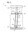
- FIG. 5 shows a first embodiment of the fastening device according to the invention.
- the bush-shaped end pieces 6a, 6b of the connecting element 6 a funnel-shaped, the clamping ring 63 forming constriction 62.
- the advantage of this embodiment is the conceivable simple production of the connecting element 6.
- a constriction is introduced by means of a crimping at the two end portions of a hollow cylindrical sleeve.
- FIG. 6 shows a second embodiment of the fastening device according to the invention.
- the connecting element 6 are pin-shaped and the two contact elements 4, 5 bush-shaped.
- the connecting element 6 shown is a wire pin having a substantially constant outer diameter.
- first contact element 4 corresponds in terms of the function and design essentially one in FIG. 1 to FIG. 4 shown connecting element 6, which is divided in the axial center M.
- second contact element 4 corresponds in terms of the function and design essentially a in FIG. 5 illustrated connecting element 6, which is divided in the axial center M.
- FIG. 7 shows a third embodiment of the fastening device according to the invention.
- the embodiment shown there differs from that in FIG. 6 in that, for example, two sleeve-shaped contact elements 4, 5, each with a funnel-shaped constriction for articulated connection with the pin-shaped connecting element 6 are used.
- FIG. 8 shows a fourth embodiment of the fastening device according to the invention.
- the connecting element 6 is a combination of the connecting element 6 according to 1 to FIG 4 and FIG. 6 ,
- the first end piece 6a of the connecting element 6 is socket-shaped and the second end piece 6b is pin-shaped.
- the first or second contact element 4, 5 is pin-shaped and the second or the first contact element 5, 4 in the form of a bush.
- the combined connecting element 6 substantially corresponds to that described in the previous figures.
- FIG. 9 shows a fifth embodiment of the fastening device according to the invention.
- the embodiment shown there differs from that according to FIG. 8 in that the first end piece 6b has a funnel-shaped constriction 62.
- this combined connecting element 6 substantially corresponds to in the FIG. 8 described.
Landscapes
- Engineering & Computer Science (AREA)
- Microelectronics & Electronic Packaging (AREA)
- Coupling Device And Connection With Printed Circuit (AREA)
- Control Of Motors That Do Not Use Commutators (AREA)
- Details Of Connecting Devices For Male And Female Coupling (AREA)
Priority Applications (3)
| Application Number | Priority Date | Filing Date | Title |
|---|---|---|---|
| DE502006007548T DE502006007548D1 (de) | 2006-12-05 | 2006-12-05 | Befestigungseinrichtung für elektronische Baugruppen sowie elektronisches Gerät mit einer derartigen Befestigungseinrichtung |
| EP06025153A EP1931187B1 (fr) | 2006-12-05 | 2006-12-05 | Dispositif de fixation pour modules électroniques ainsi qu'un appareil électronique doté d'un tel dispositif de fixation |
| AT06025153T ATE476090T1 (de) | 2006-12-05 | 2006-12-05 | Befestigungseinrichtung für elektronische baugruppen sowie elektronisches gerät mit einer derartigen befestigungseinrichtung |
Applications Claiming Priority (1)
| Application Number | Priority Date | Filing Date | Title |
|---|---|---|---|
| EP06025153A EP1931187B1 (fr) | 2006-12-05 | 2006-12-05 | Dispositif de fixation pour modules électroniques ainsi qu'un appareil électronique doté d'un tel dispositif de fixation |
Publications (2)
| Publication Number | Publication Date |
|---|---|
| EP1931187A1 true EP1931187A1 (fr) | 2008-06-11 |
| EP1931187B1 EP1931187B1 (fr) | 2010-07-28 |
Family
ID=38283165
Family Applications (1)
| Application Number | Title | Priority Date | Filing Date |
|---|---|---|---|
| EP06025153A Not-in-force EP1931187B1 (fr) | 2006-12-05 | 2006-12-05 | Dispositif de fixation pour modules électroniques ainsi qu'un appareil électronique doté d'un tel dispositif de fixation |
Country Status (3)
| Country | Link |
|---|---|
| EP (1) | EP1931187B1 (fr) |
| AT (1) | ATE476090T1 (fr) |
| DE (1) | DE502006007548D1 (fr) |
Cited By (3)
| Publication number | Priority date | Publication date | Assignee | Title |
|---|---|---|---|---|
| EP2964004A3 (fr) * | 2014-07-04 | 2016-10-12 | Karlsruher Institut für Technologie | Agencement de composant electronique |
| CN106402121A (zh) * | 2015-03-25 | 2017-02-15 | 罗伯特·博世有限公司 | 用于机械连接电子设备壳体的连接元件 |
| EP4353057B1 (fr) * | 2022-04-27 | 2025-04-23 | FRONIUS INTERNATIONAL GmbH | Module électronique pourvu d'au moins une carte de circuit imprimé et de composants électroniques externes, ainsi qu'onduleur doté d'un tel module électronique |
Citations (4)
| Publication number | Priority date | Publication date | Assignee | Title |
|---|---|---|---|---|
| FR2590104A1 (fr) | 1985-11-13 | 1987-05-15 | Legrand Sa | Module, en particulier appareillage electrique modulaire, propre a etre assemble a un autre |
| EP0626712A1 (fr) * | 1993-05-26 | 1994-11-30 | Bticino S.P.A. | Dispositif de couplage entre deux appareils électriques modulaires |
| DE19547011C1 (de) * | 1995-12-15 | 1997-01-09 | Siemens Ag | Schaltgerät |
| EP1109277A2 (fr) * | 1999-12-18 | 2001-06-20 | ABBPATENT GmbH | Elément d'accouplement de deux appareils électriques montés côte-à-côte, et méthode d'accouplement d'appareillages électriques |
-
2006
- 2006-12-05 EP EP06025153A patent/EP1931187B1/fr not_active Not-in-force
- 2006-12-05 AT AT06025153T patent/ATE476090T1/de active
- 2006-12-05 DE DE502006007548T patent/DE502006007548D1/de active Active
Patent Citations (4)
| Publication number | Priority date | Publication date | Assignee | Title |
|---|---|---|---|---|
| FR2590104A1 (fr) | 1985-11-13 | 1987-05-15 | Legrand Sa | Module, en particulier appareillage electrique modulaire, propre a etre assemble a un autre |
| EP0626712A1 (fr) * | 1993-05-26 | 1994-11-30 | Bticino S.P.A. | Dispositif de couplage entre deux appareils électriques modulaires |
| DE19547011C1 (de) * | 1995-12-15 | 1997-01-09 | Siemens Ag | Schaltgerät |
| EP1109277A2 (fr) * | 1999-12-18 | 2001-06-20 | ABBPATENT GmbH | Elément d'accouplement de deux appareils électriques montés côte-à-côte, et méthode d'accouplement d'appareillages électriques |
Cited By (3)
| Publication number | Priority date | Publication date | Assignee | Title |
|---|---|---|---|---|
| EP2964004A3 (fr) * | 2014-07-04 | 2016-10-12 | Karlsruher Institut für Technologie | Agencement de composant electronique |
| CN106402121A (zh) * | 2015-03-25 | 2017-02-15 | 罗伯特·博世有限公司 | 用于机械连接电子设备壳体的连接元件 |
| EP4353057B1 (fr) * | 2022-04-27 | 2025-04-23 | FRONIUS INTERNATIONAL GmbH | Module électronique pourvu d'au moins une carte de circuit imprimé et de composants électroniques externes, ainsi qu'onduleur doté d'un tel module électronique |
Also Published As
| Publication number | Publication date |
|---|---|
| DE502006007548D1 (de) | 2010-09-09 |
| ATE476090T1 (de) | 2010-08-15 |
| EP1931187B1 (fr) | 2010-07-28 |
Similar Documents
| Publication | Publication Date | Title |
|---|---|---|
| EP1157448B1 (fr) | Liaison coaxiale pour carte de circuits imprimes | |
| EP3262666B1 (fr) | Composant électrique et procédé de manufacture de ce composant | |
| EP1855319B1 (fr) | Module semi-conducteur à haute puissance | |
| DE10048290C5 (de) | Induktiver Sensor | |
| DE202008018126U1 (de) | Lötanschlusselement | |
| DE102005017849B4 (de) | Elektronisches Bauteil | |
| WO2005032224A1 (fr) | Carte de circuits imprimes comprenant un dispositif de maintien concu pour maintenir des composants electroniques cables, procede pour produire une telle carte de circuits imprimes et son utilisation dans un four a braser | |
| EP1931187B1 (fr) | Dispositif de fixation pour modules électroniques ainsi qu'un appareil électronique doté d'un tel dispositif de fixation | |
| DE102020100364B4 (de) | Leistungselektronische Baugruppe mit einem Substrat, einer Hülse und einem Kontaktstift und Verfahren zur Herstellung einer solchen Baugruppe | |
| EP3482465B1 (fr) | Élément de contact à conducteur interne, sollicité par un ressort | |
| DE102005021959A1 (de) | Batteriestromsensor für ein Kraftfahrzeug | |
| EP0915343A2 (fr) | Dispositif de contact facile à entretenir | |
| DE102012204069B4 (de) | Elektrische Steckerverbindung | |
| EP1535364B1 (fr) | Element d'attenuation ou de terminaison a structure coaxiale pour ondes electromagnetiques haute frequence | |
| WO2009143863A1 (fr) | Arrangement d’antenne en boîtier | |
| DE10259320B4 (de) | Druckkontaktiertes elektrisches Bauelement | |
| DE112017007766B4 (de) | Halbleitereinrichtung | |
| DE102009022659B4 (de) | Kontakteinrichtung für ein Leistungshalbleitermodul | |
| WO2022152410A1 (fr) | Connexion électrique enfichable et agencement de carte de circuit imprimé | |
| DE10047126A1 (de) | Befestigungseinrichtung | |
| DE10163574C2 (de) | Kontaktvorrichtung | |
| EP3740050A1 (fr) | Carte de circuit imprimé dotée d'un connecteur enfichable | |
| EP0735372A1 (fr) | Adaptateur de test | |
| DE102013203536B4 (de) | Vorrichtung zum Prüfen von elektronischen Bauteilen | |
| EP1921643B1 (fr) | Matrice de contact par pression |
Legal Events
| Date | Code | Title | Description |
|---|---|---|---|
| PUAI | Public reference made under article 153(3) epc to a published international application that has entered the european phase |
Free format text: ORIGINAL CODE: 0009012 |
|
| AK | Designated contracting states |
Kind code of ref document: A1 Designated state(s): AT BE BG CH CY CZ DE DK EE ES FI FR GB GR HU IE IS IT LI LT LU LV MC NL PL PT RO SE SI SK TR |
|
| AX | Request for extension of the european patent |
Extension state: AL BA HR MK RS |
|
| 17P | Request for examination filed |
Effective date: 20080710 |
|
| 17Q | First examination report despatched |
Effective date: 20080811 |
|
| AKX | Designation fees paid |
Designated state(s): AT BE BG CH CY CZ DE DK EE ES FI FR GB GR HU IE IS IT LI LT LU LV MC NL PL PT RO SE SI SK TR |
|
| GRAP | Despatch of communication of intention to grant a patent |
Free format text: ORIGINAL CODE: EPIDOSNIGR1 |
|
| GRAS | Grant fee paid |
Free format text: ORIGINAL CODE: EPIDOSNIGR3 |
|
| GRAA | (expected) grant |
Free format text: ORIGINAL CODE: 0009210 |
|
| AK | Designated contracting states |
Kind code of ref document: B1 Designated state(s): AT BE BG CH CY CZ DE DK EE ES FI FR GB GR HU IE IS IT LI LT LU LV MC NL PL PT RO SE SI SK TR |
|
| REG | Reference to a national code |
Ref country code: GB Ref legal event code: FG4D Free format text: NOT ENGLISH |
|
| REG | Reference to a national code |
Ref country code: CH Ref legal event code: EP |
|
| REG | Reference to a national code |
Ref country code: IE Ref legal event code: FG4D Free format text: LANGUAGE OF EP DOCUMENT: GERMAN |
|
| REF | Corresponds to: |
Ref document number: 502006007548 Country of ref document: DE Date of ref document: 20100909 Kind code of ref document: P |
|
| REG | Reference to a national code |
Ref country code: SE Ref legal event code: TRGR |
|
| REG | Reference to a national code |
Ref country code: NL Ref legal event code: VDEP Effective date: 20100728 |
|
| LTIE | Lt: invalidation of european patent or patent extension |
Effective date: 20100728 |
|
| PG25 | Lapsed in a contracting state [announced via postgrant information from national office to epo] |
Ref country code: FI Free format text: LAPSE BECAUSE OF FAILURE TO SUBMIT A TRANSLATION OF THE DESCRIPTION OR TO PAY THE FEE WITHIN THE PRESCRIBED TIME-LIMIT Effective date: 20100728 Ref country code: LT Free format text: LAPSE BECAUSE OF FAILURE TO SUBMIT A TRANSLATION OF THE DESCRIPTION OR TO PAY THE FEE WITHIN THE PRESCRIBED TIME-LIMIT Effective date: 20100728 Ref country code: NL Free format text: LAPSE BECAUSE OF FAILURE TO SUBMIT A TRANSLATION OF THE DESCRIPTION OR TO PAY THE FEE WITHIN THE PRESCRIBED TIME-LIMIT Effective date: 20100728 |
|
| PG25 | Lapsed in a contracting state [announced via postgrant information from national office to epo] |
Ref country code: SI Free format text: LAPSE BECAUSE OF FAILURE TO SUBMIT A TRANSLATION OF THE DESCRIPTION OR TO PAY THE FEE WITHIN THE PRESCRIBED TIME-LIMIT Effective date: 20100728 Ref country code: BG Free format text: LAPSE BECAUSE OF FAILURE TO SUBMIT A TRANSLATION OF THE DESCRIPTION OR TO PAY THE FEE WITHIN THE PRESCRIBED TIME-LIMIT Effective date: 20101028 Ref country code: CY Free format text: LAPSE BECAUSE OF FAILURE TO SUBMIT A TRANSLATION OF THE DESCRIPTION OR TO PAY THE FEE WITHIN THE PRESCRIBED TIME-LIMIT Effective date: 20100728 Ref country code: IS Free format text: LAPSE BECAUSE OF FAILURE TO SUBMIT A TRANSLATION OF THE DESCRIPTION OR TO PAY THE FEE WITHIN THE PRESCRIBED TIME-LIMIT Effective date: 20101128 Ref country code: PL Free format text: LAPSE BECAUSE OF FAILURE TO SUBMIT A TRANSLATION OF THE DESCRIPTION OR TO PAY THE FEE WITHIN THE PRESCRIBED TIME-LIMIT Effective date: 20100728 Ref country code: PT Free format text: LAPSE BECAUSE OF FAILURE TO SUBMIT A TRANSLATION OF THE DESCRIPTION OR TO PAY THE FEE WITHIN THE PRESCRIBED TIME-LIMIT Effective date: 20101129 |
|
| REG | Reference to a national code |
Ref country code: IE Ref legal event code: FD4D |
|
| PG25 | Lapsed in a contracting state [announced via postgrant information from national office to epo] |
Ref country code: LV Free format text: LAPSE BECAUSE OF FAILURE TO SUBMIT A TRANSLATION OF THE DESCRIPTION OR TO PAY THE FEE WITHIN THE PRESCRIBED TIME-LIMIT Effective date: 20100728 Ref country code: GR Free format text: LAPSE BECAUSE OF FAILURE TO SUBMIT A TRANSLATION OF THE DESCRIPTION OR TO PAY THE FEE WITHIN THE PRESCRIBED TIME-LIMIT Effective date: 20101029 |
|
| PG25 | Lapsed in a contracting state [announced via postgrant information from national office to epo] |
Ref country code: DK Free format text: LAPSE BECAUSE OF FAILURE TO SUBMIT A TRANSLATION OF THE DESCRIPTION OR TO PAY THE FEE WITHIN THE PRESCRIBED TIME-LIMIT Effective date: 20100728 Ref country code: IE Free format text: LAPSE BECAUSE OF FAILURE TO SUBMIT A TRANSLATION OF THE DESCRIPTION OR TO PAY THE FEE WITHIN THE PRESCRIBED TIME-LIMIT Effective date: 20100728 |
|
| PG25 | Lapsed in a contracting state [announced via postgrant information from national office to epo] |
Ref country code: EE Free format text: LAPSE BECAUSE OF FAILURE TO SUBMIT A TRANSLATION OF THE DESCRIPTION OR TO PAY THE FEE WITHIN THE PRESCRIBED TIME-LIMIT Effective date: 20100728 Ref country code: RO Free format text: LAPSE BECAUSE OF FAILURE TO SUBMIT A TRANSLATION OF THE DESCRIPTION OR TO PAY THE FEE WITHIN THE PRESCRIBED TIME-LIMIT Effective date: 20100728 Ref country code: SK Free format text: LAPSE BECAUSE OF FAILURE TO SUBMIT A TRANSLATION OF THE DESCRIPTION OR TO PAY THE FEE WITHIN THE PRESCRIBED TIME-LIMIT Effective date: 20100728 Ref country code: CZ Free format text: LAPSE BECAUSE OF FAILURE TO SUBMIT A TRANSLATION OF THE DESCRIPTION OR TO PAY THE FEE WITHIN THE PRESCRIBED TIME-LIMIT Effective date: 20100728 |
|
| PLBE | No opposition filed within time limit |
Free format text: ORIGINAL CODE: 0009261 |
|
| STAA | Information on the status of an ep patent application or granted ep patent |
Free format text: STATUS: NO OPPOSITION FILED WITHIN TIME LIMIT |
|
| BERE | Be: lapsed |
Owner name: SIEMENS A.G. Effective date: 20101231 |
|
| PG25 | Lapsed in a contracting state [announced via postgrant information from national office to epo] |
Ref country code: ES Free format text: LAPSE BECAUSE OF FAILURE TO SUBMIT A TRANSLATION OF THE DESCRIPTION OR TO PAY THE FEE WITHIN THE PRESCRIBED TIME-LIMIT Effective date: 20101108 |
|
| 26N | No opposition filed |
Effective date: 20110429 |
|
| PG25 | Lapsed in a contracting state [announced via postgrant information from national office to epo] |
Ref country code: MC Free format text: LAPSE BECAUSE OF NON-PAYMENT OF DUE FEES Effective date: 20101231 |
|
| REG | Reference to a national code |
Ref country code: CH Ref legal event code: PL |
|
| GBPC | Gb: european patent ceased through non-payment of renewal fee |
Effective date: 20101205 |
|
| REG | Reference to a national code |
Ref country code: DE Ref legal event code: R097 Ref document number: 502006007548 Country of ref document: DE Effective date: 20110429 |
|
| PG25 | Lapsed in a contracting state [announced via postgrant information from national office to epo] |
Ref country code: BE Free format text: LAPSE BECAUSE OF NON-PAYMENT OF DUE FEES Effective date: 20101231 |
|
| PG25 | Lapsed in a contracting state [announced via postgrant information from national office to epo] |
Ref country code: LI Free format text: LAPSE BECAUSE OF NON-PAYMENT OF DUE FEES Effective date: 20101231 Ref country code: CH Free format text: LAPSE BECAUSE OF NON-PAYMENT OF DUE FEES Effective date: 20101231 |
|
| PG25 | Lapsed in a contracting state [announced via postgrant information from national office to epo] |
Ref country code: GB Free format text: LAPSE BECAUSE OF NON-PAYMENT OF DUE FEES Effective date: 20101205 |
|
| PG25 | Lapsed in a contracting state [announced via postgrant information from national office to epo] |
Ref country code: LU Free format text: LAPSE BECAUSE OF NON-PAYMENT OF DUE FEES Effective date: 20101205 Ref country code: HU Free format text: LAPSE BECAUSE OF FAILURE TO SUBMIT A TRANSLATION OF THE DESCRIPTION OR TO PAY THE FEE WITHIN THE PRESCRIBED TIME-LIMIT Effective date: 20110129 |
|
| PG25 | Lapsed in a contracting state [announced via postgrant information from national office to epo] |
Ref country code: TR Free format text: LAPSE BECAUSE OF FAILURE TO SUBMIT A TRANSLATION OF THE DESCRIPTION OR TO PAY THE FEE WITHIN THE PRESCRIBED TIME-LIMIT Effective date: 20100728 |
|
| REG | Reference to a national code |
Ref country code: AT Ref legal event code: MM01 Ref document number: 476090 Country of ref document: AT Kind code of ref document: T Effective date: 20111205 |
|
| PGFP | Annual fee paid to national office [announced via postgrant information from national office to epo] |
Ref country code: IT Payment date: 20121220 Year of fee payment: 7 Ref country code: SE Payment date: 20121210 Year of fee payment: 7 |
|
| PGFP | Annual fee paid to national office [announced via postgrant information from national office to epo] |
Ref country code: DE Payment date: 20130218 Year of fee payment: 7 Ref country code: FR Payment date: 20130131 Year of fee payment: 7 |
|
| PG25 | Lapsed in a contracting state [announced via postgrant information from national office to epo] |
Ref country code: AT Free format text: LAPSE BECAUSE OF NON-PAYMENT OF DUE FEES Effective date: 20111205 |
|
| REG | Reference to a national code |
Ref country code: DE Ref legal event code: R119 Ref document number: 502006007548 Country of ref document: DE |
|
| REG | Reference to a national code |
Ref country code: SE Ref legal event code: EUG |
|
| PG25 | Lapsed in a contracting state [announced via postgrant information from national office to epo] |
Ref country code: SE Free format text: LAPSE BECAUSE OF NON-PAYMENT OF DUE FEES Effective date: 20131206 |
|
| REG | Reference to a national code |
Ref country code: FR Ref legal event code: ST Effective date: 20140829 |
|
| REG | Reference to a national code |
Ref country code: DE Ref legal event code: R119 Ref document number: 502006007548 Country of ref document: DE Effective date: 20140701 |
|
| PG25 | Lapsed in a contracting state [announced via postgrant information from national office to epo] |
Ref country code: DE Free format text: LAPSE BECAUSE OF NON-PAYMENT OF DUE FEES Effective date: 20140701 |
|
| PG25 | Lapsed in a contracting state [announced via postgrant information from national office to epo] |
Ref country code: FR Free format text: LAPSE BECAUSE OF NON-PAYMENT OF DUE FEES Effective date: 20131231 |
|
| PG25 | Lapsed in a contracting state [announced via postgrant information from national office to epo] |
Ref country code: IT Free format text: LAPSE BECAUSE OF NON-PAYMENT OF DUE FEES Effective date: 20131231 |
|
| PG25 | Lapsed in a contracting state [announced via postgrant information from national office to epo] |
Ref country code: IT Free format text: LAPSE BECAUSE OF NON-PAYMENT OF DUE FEES Effective date: 20131205 |