EP1933341A2 - Composant SMD inductif - Google Patents
Composant SMD inductif Download PDFInfo
- Publication number
- EP1933341A2 EP1933341A2 EP07020361A EP07020361A EP1933341A2 EP 1933341 A2 EP1933341 A2 EP 1933341A2 EP 07020361 A EP07020361 A EP 07020361A EP 07020361 A EP07020361 A EP 07020361A EP 1933341 A2 EP1933341 A2 EP 1933341A2
- Authority
- EP
- European Patent Office
- Prior art keywords
- housing
- component according
- support element
- component
- electrical connections
- Prior art date
- Legal status (The legal status is an assumption and is not a legal conclusion. Google has not performed a legal analysis and makes no representation as to the accuracy of the status listed.)
- Withdrawn
Links
Images
Classifications
-
- H—ELECTRICITY
- H01—ELECTRIC ELEMENTS
- H01F—MAGNETS; INDUCTANCES; TRANSFORMERS; SELECTION OF MATERIALS FOR THEIR MAGNETIC PROPERTIES
- H01F27/00—Details of transformers or inductances, in general
- H01F27/28—Coils; Windings; Conductive connections
- H01F27/29—Terminals; Tapping arrangements for signal inductances
- H01F27/292—Surface mounted devices
-
- H—ELECTRICITY
- H01—ELECTRIC ELEMENTS
- H01F—MAGNETS; INDUCTANCES; TRANSFORMERS; SELECTION OF MATERIALS FOR THEIR MAGNETIC PROPERTIES
- H01F27/00—Details of transformers or inductances, in general
- H01F27/02—Casings
- H01F27/027—Casings specially adapted for combination of signal type inductors or transformers with electronic circuits, e.g. mounting on printed circuit boards
-
- H—ELECTRICITY
- H05—ELECTRIC TECHNIQUES NOT OTHERWISE PROVIDED FOR
- H05K—PRINTED CIRCUITS; CASINGS OR CONSTRUCTIONAL DETAILS OF ELECTRIC APPARATUS; MANUFACTURE OF ASSEMBLAGES OF ELECTRICAL COMPONENTS
- H05K3/00—Apparatus or processes for manufacturing printed circuits
- H05K3/30—Assembling printed circuits with electric components, e.g. with resistors
- H05K3/303—Assembling printed circuits with electric components, e.g. with resistors with surface mounted components
-
- H—ELECTRICITY
- H01—ELECTRIC ELEMENTS
- H01F—MAGNETS; INDUCTANCES; TRANSFORMERS; SELECTION OF MATERIALS FOR THEIR MAGNETIC PROPERTIES
- H01F17/00—Fixed inductances of the signal type
- H01F17/04—Fixed inductances of the signal type with magnetic core
- H01F2017/048—Fixed inductances of the signal type with magnetic core with encapsulating core, e.g. made of resin and magnetic powder
-
- H—ELECTRICITY
- H05—ELECTRIC TECHNIQUES NOT OTHERWISE PROVIDED FOR
- H05K—PRINTED CIRCUITS; CASINGS OR CONSTRUCTIONAL DETAILS OF ELECTRIC APPARATUS; MANUFACTURE OF ASSEMBLAGES OF ELECTRICAL COMPONENTS
- H05K2201/00—Indexing scheme relating to printed circuits covered by H05K1/00
- H05K2201/09—Shape and layout
- H05K2201/09209—Shape and layout details of conductors
- H05K2201/09654—Shape and layout details of conductors covering at least two types of conductors provided for in H05K2201/09218 - H05K2201/095
- H05K2201/09781—Dummy conductors, i.e. not used for normal transport of current; Dummy electrodes of components
-
- H—ELECTRICITY
- H05—ELECTRIC TECHNIQUES NOT OTHERWISE PROVIDED FOR
- H05K—PRINTED CIRCUITS; CASINGS OR CONSTRUCTIONAL DETAILS OF ELECTRIC APPARATUS; MANUFACTURE OF ASSEMBLAGES OF ELECTRICAL COMPONENTS
- H05K2201/00—Indexing scheme relating to printed circuits covered by H05K1/00
- H05K2201/10—Details of components or other objects attached to or integrated in a printed circuit board
- H05K2201/10007—Types of components
- H05K2201/1003—Non-printed inductor
-
- H—ELECTRICITY
- H05—ELECTRIC TECHNIQUES NOT OTHERWISE PROVIDED FOR
- H05K—PRINTED CIRCUITS; CASINGS OR CONSTRUCTIONAL DETAILS OF ELECTRIC APPARATUS; MANUFACTURE OF ASSEMBLAGES OF ELECTRICAL COMPONENTS
- H05K3/00—Apparatus or processes for manufacturing printed circuits
- H05K3/30—Assembling printed circuits with electric components, e.g. with resistors
- H05K3/32—Assembling printed circuits with electric components, e.g. with resistors electrically connecting electric components or wires to printed circuits
- H05K3/34—Assembling printed circuits with electric components, e.g. with resistors electrically connecting electric components or wires to printed circuits by soldering
- H05K3/341—Surface mounted components
- H05K3/3421—Leaded components
-
- Y—GENERAL TAGGING OF NEW TECHNOLOGICAL DEVELOPMENTS; GENERAL TAGGING OF CROSS-SECTIONAL TECHNOLOGIES SPANNING OVER SEVERAL SECTIONS OF THE IPC; TECHNICAL SUBJECTS COVERED BY FORMER USPC CROSS-REFERENCE ART COLLECTIONS [XRACs] AND DIGESTS
- Y02—TECHNOLOGIES OR APPLICATIONS FOR MITIGATION OR ADAPTATION AGAINST CLIMATE CHANGE
- Y02P—CLIMATE CHANGE MITIGATION TECHNOLOGIES IN THE PRODUCTION OR PROCESSING OF GOODS
- Y02P70/00—Climate change mitigation technologies in the production process for final industrial or consumer products
- Y02P70/50—Manufacturing or production processes characterised by the final manufactured product
Definitions
- the invention relates to an inductive SMD component (SMD: surface mounted device) with an inductive element in a housing, and an arrangement of an electrical circuit board and the inductive SMD component.
- SMD surface mounted device
- SMT surface-mounting technology
- PTH pin through hole
- SMD components are soldered on one side only to the pads of a printed circuit board, saving material and reducing the size of electronic circuits.
- a printed circuit board can be equipped on both sides.
- the SMD component is not fixed on the printed circuit board prior to the production of a solder connection between an SMD component and the SMT circuit board, with secure positioning of the SMD component solely via the contact surface of the connection of the SMD component and the SMT board is not guaranteed. Due to the limited SMT contact surface per connection results in particular in a throttle with only two electrical connections at their ends so far the problem that this must be laboriously positioned on a circuit board in order to be reliably soldered can.
- the present invention is based on the object, a suitable for SMT assembly and safe with little effort to provide positionable inductive component with two electrical connections, as well as an arrangement with such a component and a circuit board.
- the object is achieved in that in addition to two existing terminals of an inductive element, a relative to the inductive element fixed support member is provided on the component in the component.
- the end of the support element leading away from the inductive element forms a mounting surface outside the component with the ends of the electrical connections.
- a mounting plane of the component the plane is considered, which is formed after the SMT assembly by the component facing side of the printed circuit board to be contacted.
- inductive elements in addition to coils with magnetic cores air coils, wound films, strip conductors, etc. can be used.
- One aspect of the invention is that the contact areas of the terminal ends on the printed circuit board do not lie in a line, but form a triangle, no matter how many electrical connections are present. With only two electrical connections, without the presence of a support element, positioning the device on an SMT board would be difficult because the device would threaten to fall over. Also, more than two connection elements can be unfavorable for the stability of the component, for example, when the connection elements are arranged in a line. Also in this case, the additional provision of a support element outside this line can be useful for mounting a mounting surface.
- bearing areas it is advantageous if all bearing areas are aligned as coplanar as possible to the defined mounting surface. But it can also be provided that the support areas are not flat, but each with a circuit board facing tip or edge are formed to each other by the thus formed tapering space between the support area and the circuit board to form a space in which liquid soldering material is sucked in by the surface tension. Also in this case, it is advantageous to allow a defined position of the SMD component on a circuit board by means of a support element.
- an adhesive or a solder paste can be used, which are placed before the application of the component, for example by means of a screen printing method or by applying a thin tube. Thereafter, for example, by means of a programmable placement machine, a component is placed and then this conductively connected to the printed circuit with heat.
- the solder paste used typically contains a mixture of a flux and very small solder balls.
- soldering of SMD components various soldering methods are known, in which case, in particular, the reflow soldering method can be used favorably.
- the soldering provides both an electrical and a mechanical connection.
- the so-called tombstoning has been found in which components are subjected as part of their soldering by asymmetric action of the surface tension of the liquefied solder of a force that the corresponding component tilts out of the circuit board level and leads to non-contacted terminals.
- the support element consists of an electrically conductive material.
- the support element as well as the electrical connections for example, consist of an electrically conductive wire, which may be bent to form support areas at its end. This can be the case both in the support element and in the electrical connection elements, wherein the bend can advantageously be provided at right angles.
- connection elements can also be designed as strip-shaped conductors. At the ends of the conductors may be provided instead of bent wire ends and widened metal pads, similar to those provided on the corresponding circuit boards.
- the soldering of the support areas on mostly round pads of the circuit board is centered due to the surface tension of the liquefied solder used. This effect is exacerbated when the support areas of the component are formed as round pads.
- the support element can be attached directly to the inductive element. This has the advantage that the positioning of the electrical connections and support areas of the inductive element are fixed relative to the support element and are stable.
- the component has a stabilizing element connected to the inductive element.
- a stabilizing element can be for example a housing body or a potting compound connected to the inductive element or another stabilizing body, for example a plate, to which the inductive element is glued.
- Such stabilizing elements can on the one hand serve to protect the inductive element on the circuit board, on the other hand also to make the inductive element transportable and shield in the SMT assembly against external influences, since some inductive elements are so unstable that they require mechanical protection.
- the component may for example comprise a housing made of a conductive material, wherein the material may be processed, for example as a powder metallic material by pressing or sintering and also may also have soft magnetic properties.
- the material of the housing can also take over magnetic properties in connection with the inductive element.
- the conductive property of the material can serve to shield the inductive element or to place the housing at ground potential by means of the support element.
- the stabilizing element may have a potting compound, in which the inductive element is embedded.
- the potting compound may be provided alone as a stabilizing element or in turn be surrounded by the housing.
- the potting compound may for example consist of a soft magnetic material to cooperate in the function of the inductive element with this, in particular, if it is a coil, in the desired manner.
- the support member may for example be attached to the housing or even connected in one piece and made of the same material as this.
- the support element may for example also be produced in a single production step together with the housing.
- the support member may also be partially poured into the potting compound and connected in this way with the inductive element or one of the parts of the stabilizing element may have a receptacle for fixing and positioning of the support element, in which this is insertable and in which it can be fixed, for example by gluing ,
- This may, for example, simply be a hole in the potting compound or in the housing, into which a pin of the support element can be inserted.
- the stabilizing element may have a shell core of a soft magnetic material, which influences the magnetic flux lines of the air coil in a desired manner.
- the shell core may have a pin passing through the inductive element.
- the shell core is advantageously designed in several parts, so that it can be wrapped around this after the provision of the inductive element.
- the invention also relates to an arrangement of an electrical circuit board and an inductive SMD component, wherein at least the electrical connections of the inductive element are soldered to the circuit board by SMT technology, whereby an electrical and mechanical connection is created.
- a support element can either rest unsoldered on the circuit board, whereby it ensures during the assembly process by its supporting and positioning effect for a positionally accurate fixation of the component or the support element can be soldered as well as the electrical connections of the inductive element to the circuit board and so for an additional Stabilize the connection. additionally
- the supporting element can also cause the housing, as part of the stabilizing element, to be connected to a specific desired potential.
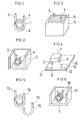
- FIG. 1 shows as an example of an inductive element 1, an electric coil, which consists of a simple conductor 2 with several turns and two electrical terminals 3, 4, but no core of magnetically active, such as soft magnetic, material has, which is generally referred to as an air coil ,
- Such coils can be embedded as inductive elements in a potting compound or produced in a housing both as classic electronic components for the PTH technique (pin through hole) and as SMD components.
- FIG. 2 shows a coil, as in FIG. 1 is shown, in a housing 5, in which the coil is glued or cast, for example, such that the electrical connections 3, 4 protrude.
- the housing may for example consist of an insulating material to electrically energize the coil isolate, alternatively, from a conductive material, so that the housing can be placed, for example at ground potential.
- FIG. 3 In the FIG. 3 is the component made FIG. 2 shown shed, with a casting material 6 is shown hatched.
- Both the material of the housing 5 and the casting material may have special magnetic properties, for example, be soft magnetic.
- the properties of the inductive element as far as it is an inductive element as in the present example, can be selectively influenced.
- the housing 5 may for example be made of a powder metallurgical material by pressing or sintering.
- FIG. 4 shows an electronic component 7 with an inductive element 2 in the form of a coil, from which the electrical connections 3, 4 protrude, wherein the component 7 is shown floating over a printed circuit board 8.
- the printed circuit board 8 corresponds to the conventional, conventional PTH (pin through hole) technique and has bores 9, 10 for receiving the electrical connections 3, 4.
- PTH pin through hole
- An inductive component as in the FIGS. 1 to 4 is illustrated, could in principle also be produced as an SMD component.
- a prerequisite is that the terminals 13, 14 have such contact areas, which allow the plant to the surface of an electrical circuit board for the purpose of soldering.
- the SMD component must first be positioned on the circuit board before the actual Soldering takes place.
- the component can first be glued or fixed by means of a solder paste, but remains a certain uncertainty that the component changes its position by tilting. This is especially a problem when there are only two electrical connections that are naturally in line and do not span a mounting surface, such as a coil. But even with more than two electrical connections, these can lie in a line or close to each other, so that an additional support element according to the invention has the advantageous effect of better support.
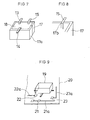
- the support element will be positioned relative to the inductive element or the rest of the support areas so that a mounting surface is clamped.
- both the electrical connections 13, 14 as well as in the FIG. 5 designated 15 supporting member which terminates in a connecting wire 16, bent to form support areas at right angles.
- the electrical connections 13, 14 and the support element 15 may consist of enameled wires, wherein the wire ends of the electrical connections (13, 14) and the support element 15 are advantageously either stripped or stripped and tinned.
- Suitable materials for the leads are Cu, Cu alloys such as CuSn 6 or other conductive materials in question.
- inductive element 1 and the support member 15 are shown together in a housing part 17, which in turn together with another, for example mirror-symmetrically attached housing part 17a forms an overall housing for receiving the inductive element 1 and the support element 15.
- Such a component in already finished potted state is in the FIG. 7 shown, where there already the support areas by right-angled bending of the terminals 13, 14 and the support element 15 are formed.
- the electrical connections 13, 14 and the support element 15 extend bent at the edges of the open side of the housing 17 away from the inductive element 1 in the mounting plane.
- the ends of the electrical connections 13, 14 and of the support element 15 bent into the mounting plane are in contact with the housing 17, 25.
- the electrical terminals 13, 14 and the support element 15 may also be bent to the inductive element 1 leading in the mounting plane, for example as J-shaped elements (J-leads).
- the potting material 18 does not fill the housing 17, 17 a completely, so that a disability can be excluded by the potting material 18 when placing the component on a circuit board.
- Suitable potting materials are, for example, epoxy, pure or silicone. Other materials are possible.
- a recess 17b is shown in the housing 17 in which a curved support member 15 extends.
- the recess 17 causes in addition to the in FIG. 7 Guide shown by the edges of the housing 17 is a guide of the support member 15 in the plane of the open side of the housing 17.
- the recess 17b is open in the direction of the normal on the level of the open side of the housing 17 of the inductive element 1 (not shown ) leading away. In cross section, the recess 17b may have a substantially round or semicircular shape. Due to the course of the support element 15 below the housing edge, the support member 15 is not outside the housing 17. In course of the electrical contacts 13, 14 (not shown) in guides 17b, the housing 17 can rest flat on the mounting surface.
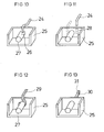
- the three angled bearing areas of the electrical connections and the support element span a mounting surface which lies below the housing and faces the circuit board. This is clearer in the FIG. 9 shown where a component 19 is shown floating with correspondingly formed electrical connections and a support element over a printed circuit board 20.
- solder pads 21, 22, 23 is applied to the soldering paste during the manufacturing process, for example by means of a screen printing method, before the component 19 is placed. Thereafter, the arrangement is heated at least for a short time, so that the solder balls melt in the solder paste and a solder connection is made at least in the region of the electrical connections.
- the support element can be soldered to increase the supporting action.
- FIG. 9 On the printed circuit board 20 and printed conductors 21a, 22a, 23a are shown, which are arranged on the side facing the component of the printed circuit board. This has the consequence that on the underside of the circuit board 20, a similar arrangement can be additionally arranged with other components.
- the provision according to the invention of a support element 15 under the component 19 has the consequence that the component can be permanently and safely positioned on the printed circuit board 20. For a stable positioning, a plurality of supporting elements can be mounted next to the electrical connections under the component 15.
- FIG. 10 a variant is shown which shows the attachment of a support element 24 to a housing 25 by means of a receiving bore 26.
- the bore 26 is provided in a slug 27, which may be integrally connected to the housing 25 and also may consist of a soft magnetic material.
- a corresponding receptacle 28 as in the FIG. 11 also be arranged in a housing wall of the housing 25.
- the support element 29 of the FIG. 12 can advantageously be attached to the housing 25 with a loop which is clamped on the slug 27.
- the support element 29 may be formed, for example, by a wire bent into a loop. This is shed after being pushed onto the slug 27 with the (not shown) inductive element together.
- the support member 30 is directly connected to the housing 25 in one piece.
- the support member 30 may be pressed as a web with a cranked head 31 directly to the housing material 25.
- the housing material 25 may also be wholly or partially solderable, in order to be able to fix the support element 30 to the housing in this way.
- the right-angled bends of the electrical connections 3, 4, 13, 14 are then designed such that the cranked head 31 of the support element 30 lies in a mounting surface, which is advantageously parallel to the underside of the housing 25.
- the assembly of SMT printed circuit boards is simplified and SMD components are easier and with lower loss rate than previously used without much design effort.
Landscapes
- Engineering & Computer Science (AREA)
- Power Engineering (AREA)
- Manufacturing & Machinery (AREA)
- Microelectronics & Electronic Packaging (AREA)
- Coils Or Transformers For Communication (AREA)
Applications Claiming Priority (1)
| Application Number | Priority Date | Filing Date | Title |
|---|---|---|---|
| DE102006058336A DE102006058336A1 (de) | 2006-12-11 | 2006-12-11 | Induktives SMD-Bauteil |
Publications (2)
| Publication Number | Publication Date |
|---|---|
| EP1933341A2 true EP1933341A2 (fr) | 2008-06-18 |
| EP1933341A3 EP1933341A3 (fr) | 2009-04-29 |
Family
ID=39092809
Family Applications (1)
| Application Number | Title | Priority Date | Filing Date |
|---|---|---|---|
| EP07020361A Withdrawn EP1933341A3 (fr) | 2006-12-11 | 2007-10-18 | Composant SMD inductif |
Country Status (2)
| Country | Link |
|---|---|
| EP (1) | EP1933341A3 (fr) |
| DE (1) | DE102006058336A1 (fr) |
Cited By (3)
| Publication number | Priority date | Publication date | Assignee | Title |
|---|---|---|---|---|
| DE102013208176A1 (de) * | 2013-05-03 | 2014-11-20 | Robert Bosch Gmbh | Stabkerndrossel |
| WO2018135357A1 (fr) * | 2017-01-17 | 2018-07-26 | 株式会社オートネットワーク技術研究所 | Bobine à étages multiples et structure de circuit |
| US20190378641A1 (en) * | 2017-01-26 | 2019-12-12 | Samsung Electronics Co., Ltd. | Inductor and inductor manufacturing method |
Family Cites Families (5)
| Publication number | Priority date | Publication date | Assignee | Title |
|---|---|---|---|---|
| DE3477438D1 (en) * | 1984-03-23 | 1989-04-27 | Siemens Ag | Electronic component, in particular a chip inductance |
| DE4206813A1 (de) * | 1992-03-04 | 1993-09-09 | Siemens Matsushita Components | Induktives bauelement |
| JP2002043131A (ja) * | 2000-07-25 | 2002-02-08 | Taiyo Yuden Co Ltd | インダクタンス素子及びインダクタンス素子の製造方法 |
| EP1752997B1 (fr) * | 2004-06-04 | 2010-10-20 | Sumida Corporation | Bobine d'inductance |
| DE102004048030A1 (de) * | 2004-09-29 | 2006-03-30 | Robert Bosch Gmbh | Elektrische Drosselspule |
-
2006
- 2006-12-11 DE DE102006058336A patent/DE102006058336A1/de not_active Withdrawn
-
2007
- 2007-10-18 EP EP07020361A patent/EP1933341A3/fr not_active Withdrawn
Cited By (3)
| Publication number | Priority date | Publication date | Assignee | Title |
|---|---|---|---|---|
| DE102013208176A1 (de) * | 2013-05-03 | 2014-11-20 | Robert Bosch Gmbh | Stabkerndrossel |
| WO2018135357A1 (fr) * | 2017-01-17 | 2018-07-26 | 株式会社オートネットワーク技術研究所 | Bobine à étages multiples et structure de circuit |
| US20190378641A1 (en) * | 2017-01-26 | 2019-12-12 | Samsung Electronics Co., Ltd. | Inductor and inductor manufacturing method |
Also Published As
| Publication number | Publication date |
|---|---|
| DE102006058336A1 (de) | 2008-06-19 |
| EP1933341A3 (fr) | 2009-04-29 |
Similar Documents
| Publication | Publication Date | Title |
|---|---|---|
| DE19735409A1 (de) | Leiterplatine sowie zugehöriges Kontaktelement | |
| DE3854437T2 (de) | Chipkondensator. | |
| DE3010876A1 (de) | Verfahren zur herstellung einer leiterplatte | |
| EP1933341A2 (fr) | Composant SMD inductif | |
| EP1128476A2 (fr) | Connecteur et procédé de fabrication d'un connecteur | |
| DE19625934C1 (de) | Elektrischer Leiter | |
| DE3738545A1 (de) | Einrichtung zur befestigung von steckverbindern an leiterplatten | |
| DE3910750C2 (de) | Anschlußvorrichtung für ein elektronisches Bauelement | |
| DE19726856C1 (de) | Flachstecker für elektrische Steckverbindungen | |
| DE102004049575B4 (de) | Elektrisches Anschlusselement und Verfahren zum Anschließen eines Leiterkabels | |
| DE29904493U1 (de) | Auf einer Leiterplatte montierbare Stiftleiste mit abgewinkelten Kontaktstiften | |
| DE10038424A1 (de) | Elektronisches Bauelement mit Anschluss und Anschlussklemme | |
| WO2006013145A1 (fr) | Plaquette a elements smd et au moins un element cable, et procede pour rapporter, fixer et mettre en contact electriquement des elements | |
| EP1205951B1 (fr) | Procédé pour contacter le fil d'enroulement d'une bobine avec une broche | |
| DE202013104811U1 (de) | Elektrische Kontaktvorrichtung, insbesondere elektrische Printklemme und/oder Grundleiste | |
| DE19813527C1 (de) | SMD-Kunststoffkörper für Bauelemente | |
| WO2015024715A1 (fr) | Borne de connexion électrique pour circuit imprimé | |
| CH698875B1 (de) | Verfahren zur Bestückung einer Leiterplatte mit einem Stecker. | |
| DE202004020191U1 (de) | Einschub-Kontaktierung mittels Schneidklemme | |
| DE19543765B4 (de) | Verfahren zur Herstellung von Kontaktzungen und deren Verbindung in an der Unterseite eines elektrischen Bauelements vergesehenen Anschlußstiften | |
| DD131612B1 (de) | Anordnung zur durchkontaktierung von leiterplatten | |
| AT412935B (de) | Kontaktierung von leiterplatten bzw. schaltungsträgern | |
| EP3379906B1 (fr) | Procédé de fabrication d'une connexions à fil avec une structure de support, et composant électronique associé | |
| DE3802441A1 (de) | Vorrichtung zur befestigung von netzanschlusslitzen bei auf leiterplatten angeordneten schaltungen | |
| DE10349956A1 (de) | Leiterplatte mit mindestens einem Bauteil |
Legal Events
| Date | Code | Title | Description |
|---|---|---|---|
| PUAI | Public reference made under article 153(3) epc to a published international application that has entered the european phase |
Free format text: ORIGINAL CODE: 0009012 |
|
| AK | Designated contracting states |
Kind code of ref document: A2 Designated state(s): AT BE BG CH CY CZ DE DK EE ES FI FR GB GR HU IE IS IT LI LT LU LV MC MT NL PL PT RO SE SI SK TR |
|
| AX | Request for extension of the european patent |
Extension state: AL BA HR MK RS |
|
| PUAL | Search report despatched |
Free format text: ORIGINAL CODE: 0009013 |
|
| AK | Designated contracting states |
Kind code of ref document: A3 Designated state(s): AT BE BG CH CY CZ DE DK EE ES FI FR GB GR HU IE IS IT LI LT LU LV MC MT NL PL PT RO SE SI SK TR |
|
| AX | Request for extension of the european patent |
Extension state: AL BA HR MK RS |
|
| AKX | Designation fees paid | ||
| STAA | Information on the status of an ep patent application or granted ep patent |
Free format text: STATUS: THE APPLICATION IS DEEMED TO BE WITHDRAWN |
|
| 18D | Application deemed to be withdrawn |
Effective date: 20091030 |
|
| REG | Reference to a national code |
Ref country code: DE Ref legal event code: 8566 |