EP1933609A1 - Structure de substrat - Google Patents
Structure de substrat Download PDFInfo
- Publication number
- EP1933609A1 EP1933609A1 EP06714109A EP06714109A EP1933609A1 EP 1933609 A1 EP1933609 A1 EP 1933609A1 EP 06714109 A EP06714109 A EP 06714109A EP 06714109 A EP06714109 A EP 06714109A EP 1933609 A1 EP1933609 A1 EP 1933609A1
- Authority
- EP
- European Patent Office
- Prior art keywords
- substrate
- display device
- substrate structure
- electronic components
- resin part
- Prior art date
- Legal status (The legal status is an assumption and is not a legal conclusion. Google has not performed a legal analysis and makes no representation as to the accuracy of the status listed.)
- Withdrawn
Links
Images







Classifications
-
- H—ELECTRICITY
- H05—ELECTRIC TECHNIQUES NOT OTHERWISE PROVIDED FOR
- H05K—PRINTED CIRCUITS; CASINGS OR CONSTRUCTIONAL DETAILS OF ELECTRIC APPARATUS; MANUFACTURE OF ASSEMBLAGES OF ELECTRICAL COMPONENTS
- H05K3/00—Apparatus or processes for manufacturing printed circuits
- H05K3/22—Secondary treatment of printed circuits
- H05K3/28—Applying non-metallic protective coatings
- H05K3/284—Applying non-metallic protective coatings for encapsulating mounted components
-
- H—ELECTRICITY
- H05—ELECTRIC TECHNIQUES NOT OTHERWISE PROVIDED FOR
- H05K—PRINTED CIRCUITS; CASINGS OR CONSTRUCTIONAL DETAILS OF ELECTRIC APPARATUS; MANUFACTURE OF ASSEMBLAGES OF ELECTRICAL COMPONENTS
- H05K9/00—Screening of apparatus or components against electric or magnetic fields
-
- H—ELECTRICITY
- H05—ELECTRIC TECHNIQUES NOT OTHERWISE PROVIDED FOR
- H05K—PRINTED CIRCUITS; CASINGS OR CONSTRUCTIONAL DETAILS OF ELECTRIC APPARATUS; MANUFACTURE OF ASSEMBLAGES OF ELECTRICAL COMPONENTS
- H05K3/00—Apparatus or processes for manufacturing printed circuits
- H05K3/22—Secondary treatment of printed circuits
- H05K3/28—Applying non-metallic protective coatings
-
- H—ELECTRICITY
- H05—ELECTRIC TECHNIQUES NOT OTHERWISE PROVIDED FOR
- H05K—PRINTED CIRCUITS; CASINGS OR CONSTRUCTIONAL DETAILS OF ELECTRIC APPARATUS; MANUFACTURE OF ASSEMBLAGES OF ELECTRICAL COMPONENTS
- H05K7/00—Constructional details common to different types of electric apparatus
- H05K7/20—Modifications to facilitate cooling, ventilating, or heating
- H05K7/2039—Modifications to facilitate cooling, ventilating, or heating characterised by the heat transfer by conduction from the heat generating element to a dissipating body
- H05K7/20436—Inner thermal coupling elements in heat dissipating housings, e.g. protrusions or depressions integrally formed in the housing
- H05K7/20445—Inner thermal coupling elements in heat dissipating housings, e.g. protrusions or depressions integrally formed in the housing the coupling element being an additional piece, e.g. thermal standoff
- H05K7/20463—Filling compound, e.g. potted resin
-
- H—ELECTRICITY
- H05—ELECTRIC TECHNIQUES NOT OTHERWISE PROVIDED FOR
- H05K—PRINTED CIRCUITS; CASINGS OR CONSTRUCTIONAL DETAILS OF ELECTRIC APPARATUS; MANUFACTURE OF ASSEMBLAGES OF ELECTRICAL COMPONENTS
- H05K9/00—Screening of apparatus or components against electric or magnetic fields
- H05K9/0007—Casings
- H05K9/0047—Casings being rigid plastic containers having conductive particles, fibres or mesh embedded therein
-
- H—ELECTRICITY
- H05—ELECTRIC TECHNIQUES NOT OTHERWISE PROVIDED FOR
- H05K—PRINTED CIRCUITS; CASINGS OR CONSTRUCTIONAL DETAILS OF ELECTRIC APPARATUS; MANUFACTURE OF ASSEMBLAGES OF ELECTRICAL COMPONENTS
- H05K9/00—Screening of apparatus or components against electric or magnetic fields
- H05K9/0073—Shielding materials
- H05K9/0081—Electromagnetic shielding materials, e.g. EMI, RFI shielding
- H05K9/0086—Electromagnetic shielding materials, e.g. EMI, RFI shielding comprising a single discontinuous metallic layer on an electrically insulating supporting structure, e.g. metal grid, perforated metal foil, film, aggregated flakes, sintering
-
- H—ELECTRICITY
- H05—ELECTRIC TECHNIQUES NOT OTHERWISE PROVIDED FOR
- H05K—PRINTED CIRCUITS; CASINGS OR CONSTRUCTIONAL DETAILS OF ELECTRIC APPARATUS; MANUFACTURE OF ASSEMBLAGES OF ELECTRICAL COMPONENTS
- H05K1/00—Printed circuits
- H05K1/02—Details
- H05K1/0201—Thermal arrangements, e.g. for cooling, heating or preventing overheating
- H05K1/0203—Cooling of mounted components
-
- H—ELECTRICITY
- H05—ELECTRIC TECHNIQUES NOT OTHERWISE PROVIDED FOR
- H05K—PRINTED CIRCUITS; CASINGS OR CONSTRUCTIONAL DETAILS OF ELECTRIC APPARATUS; MANUFACTURE OF ASSEMBLAGES OF ELECTRICAL COMPONENTS
- H05K1/00—Printed circuits
- H05K1/02—Details
- H05K1/0213—Electrical arrangements not otherwise provided for
- H05K1/0216—Reduction of cross-talk, noise or electromagnetic interference
- H05K1/0218—Reduction of cross-talk, noise or electromagnetic interference by printed shielding conductors, ground planes or power plane
-
- H—ELECTRICITY
- H05—ELECTRIC TECHNIQUES NOT OTHERWISE PROVIDED FOR
- H05K—PRINTED CIRCUITS; CASINGS OR CONSTRUCTIONAL DETAILS OF ELECTRIC APPARATUS; MANUFACTURE OF ASSEMBLAGES OF ELECTRICAL COMPONENTS
- H05K1/00—Printed circuits
- H05K1/02—Details
- H05K1/0274—Optical details, e.g. printed circuits comprising integral optical means
-
- H—ELECTRICITY
- H05—ELECTRIC TECHNIQUES NOT OTHERWISE PROVIDED FOR
- H05K—PRINTED CIRCUITS; CASINGS OR CONSTRUCTIONAL DETAILS OF ELECTRIC APPARATUS; MANUFACTURE OF ASSEMBLAGES OF ELECTRICAL COMPONENTS
- H05K2201/00—Indexing scheme relating to printed circuits covered by H05K1/00
- H05K2201/02—Fillers; Particles; Fibers; Reinforcement materials
- H05K2201/0203—Fillers and particles
- H05K2201/0206—Materials
- H05K2201/0209—Inorganic, non-metallic particles
-
- H—ELECTRICITY
- H05—ELECTRIC TECHNIQUES NOT OTHERWISE PROVIDED FOR
- H05K—PRINTED CIRCUITS; CASINGS OR CONSTRUCTIONAL DETAILS OF ELECTRIC APPARATUS; MANUFACTURE OF ASSEMBLAGES OF ELECTRICAL COMPONENTS
- H05K2201/00—Indexing scheme relating to printed circuits covered by H05K1/00
- H05K2201/02—Fillers; Particles; Fibers; Reinforcement materials
- H05K2201/0203—Fillers and particles
- H05K2201/0206—Materials
- H05K2201/0215—Metallic fillers
-
- H—ELECTRICITY
- H05—ELECTRIC TECHNIQUES NOT OTHERWISE PROVIDED FOR
- H05K—PRINTED CIRCUITS; CASINGS OR CONSTRUCTIONAL DETAILS OF ELECTRIC APPARATUS; MANUFACTURE OF ASSEMBLAGES OF ELECTRICAL COMPONENTS
- H05K2201/00—Indexing scheme relating to printed circuits covered by H05K1/00
- H05K2201/10—Details of components or other objects attached to or integrated in a printed circuit board
- H05K2201/10007—Types of components
- H05K2201/10128—Display
-
- H—ELECTRICITY
- H05—ELECTRIC TECHNIQUES NOT OTHERWISE PROVIDED FOR
- H05K—PRINTED CIRCUITS; CASINGS OR CONSTRUCTIONAL DETAILS OF ELECTRIC APPARATUS; MANUFACTURE OF ASSEMBLAGES OF ELECTRICAL COMPONENTS
- H05K2201/00—Indexing scheme relating to printed circuits covered by H05K1/00
- H05K2201/10—Details of components or other objects attached to or integrated in a printed circuit board
- H05K2201/10431—Details of mounted components
- H05K2201/10507—Involving several components
- H05K2201/10515—Stacked components
-
- H—ELECTRICITY
- H05—ELECTRIC TECHNIQUES NOT OTHERWISE PROVIDED FOR
- H05K—PRINTED CIRCUITS; CASINGS OR CONSTRUCTIONAL DETAILS OF ELECTRIC APPARATUS; MANUFACTURE OF ASSEMBLAGES OF ELECTRICAL COMPONENTS
- H05K2201/00—Indexing scheme relating to printed circuits covered by H05K1/00
- H05K2201/20—Details of printed circuits not provided for in H05K2201/01 - H05K2201/10
- H05K2201/2054—Light-reflecting surface, e.g. conductors, substrates, coatings, dielectrics
-
- H—ELECTRICITY
- H05—ELECTRIC TECHNIQUES NOT OTHERWISE PROVIDED FOR
- H05K—PRINTED CIRCUITS; CASINGS OR CONSTRUCTIONAL DETAILS OF ELECTRIC APPARATUS; MANUFACTURE OF ASSEMBLAGES OF ELECTRICAL COMPONENTS
- H05K2203/00—Indexing scheme relating to apparatus or processes for manufacturing printed circuits covered by H05K3/00
- H05K2203/13—Moulding and encapsulation; Deposition techniques; Protective layers
- H05K2203/1305—Moulding and encapsulation
- H05K2203/1316—Moulded encapsulation of mounted components
-
- H—ELECTRICITY
- H05—ELECTRIC TECHNIQUES NOT OTHERWISE PROVIDED FOR
- H05K—PRINTED CIRCUITS; CASINGS OR CONSTRUCTIONAL DETAILS OF ELECTRIC APPARATUS; MANUFACTURE OF ASSEMBLAGES OF ELECTRICAL COMPONENTS
- H05K2203/00—Indexing scheme relating to apparatus or processes for manufacturing printed circuits covered by H05K3/00
- H05K2203/13—Moulding and encapsulation; Deposition techniques; Protective layers
- H05K2203/1305—Moulding and encapsulation
- H05K2203/1322—Encapsulation comprising more than one layer
-
- H—ELECTRICITY
- H10—SEMICONDUCTOR DEVICES; ELECTRIC SOLID-STATE DEVICES NOT OTHERWISE PROVIDED FOR
- H10W—GENERIC PACKAGES, INTERCONNECTIONS, CONNECTORS OR OTHER CONSTRUCTIONAL DETAILS OF DEVICES COVERED BY CLASS H10
- H10W90/00—Package configurations
- H10W90/701—Package configurations characterised by the relative positions of pads or connectors relative to package parts
- H10W90/721—Package configurations characterised by the relative positions of pads or connectors relative to package parts of bump connectors
- H10W90/724—Package configurations characterised by the relative positions of pads or connectors relative to package parts of bump connectors between a chip and a stacked insulating package substrate, interposer or RDL
Definitions
- This invention relates to a substrate structure wherein plural electronic components are mounted along a substrate, the electronic components are coated with a resin part, and the resin part is in close contact with the substrate.
- a plurality of electronic components 202 that are mounted on a substrate 201 are collectively coated with a resin part 203 in such substrate structure 200.
- a display device 206 such as an LCD to be provided on a mobile terminal 205 is disposed at a position corresponding to an opening 209 provided on a housing 208 by being supported by a support member 207 that is provided on the substrate 201 in such a fashion as to stride over the resin part 203.
- the display device 206 is obtainable by laminating a main body 211, an optical sheet 212, a light guiding plate 213, a reflection sheet 214, and the like and is housed in a frame part 216 of the support member 207.
- a terminal 219 is drawn out from a liquid crystal part (not shown) disposed between a pair of transparent substrates 218.
- a light guiding part 222 that is increased in thickness so as to form a substantially wedge-like shape in accordance with a form and a size of an LED 221 serving as a light source is provided.
- the light guiding part 222 is disposed in such a fashion as to rise along an identical plane with a lower surface of the light guiding plate 213 and toward the transparent substrates 218.
- an electronic component required to have an electrical shielding property and an electronic component required to have a heat discharge property, i.e. electronic components having a high heat generating property, have been known.
- the conventional substrate structure 200 has the primary object of ensuring the mounting strength of the electronic components 202 and the function as a reinforcing material for maintaining the flatness of the substrate 201, the above-mentioned shielding property and the heat discharge property thereof is insufficient.
- Patent Publication 1 Japanese Patent No. 3241669
- Patent Publication 1 Since a plurality of notches are provided on the reinforcing frame in Patent Publication 1, Patent Publication 1 fails to achieve the satisfactory shielding property,
- the primary object of the Patent Publication 1 is to fix the lC package on the mother board, the electronic components having heat discharge property are not considered in the Patent Publication 1.
- the demand for downsizing, thinning, and reduction in number of components of the housing 208 of the mobile terminal 206 is becoming complicated since the presence of the support member 207 or the support structure of the display device 206 serves as impediment for downsizing, thinning, and reducing components of the housing 208.
- the terminal 219 of the liquid crystal part and the LED 221 of the light guiding plate 213 come close to each other, thereby raising a risk of contact.
- a structure wherein the light guiding part 222 is disposed in such a fashion as to rise toward a direction departing from the transparent substrates 218, and a recessed part or a hole for housing the light guiding part 222 is formed on a platform of the support member may be considered.
- the structure of forming the recessed part and the hole is not preferable from the viewpoint of strength.
- a structure wherein the electronic components 202 are mounted on a reverse side of the substrate 201, the light guiding part is disposed in such a fashion as to rise toward the direction departing from the transparent substrates, and a recessed part or a hole for housing the light guiding part is formed on a platform of the support member may be considered.
- Such substrate structure 200 raise a problem of not contributing to an overall thinning even when the display device 206 is directly supported on the surface of the substrate 201, since the electronic components 202 are mounted on the reverse side of the substrate 201.
- This invention has been accomplished in order to solve the above-described conventional problems, and a first object thereof is to provide a substrate structure ensuring a shielding property and a heat discharge property of a resin part that collectively covers a plurality of electronic components and capable of downsizing, thinning, and reducing the number of components.
- a second object of this invention is to provide a substrate structure less subject to damage when a load is applied on a lamination member and capable of improving strength as compared to conventional examples.
- a substrate structure of this invention comprises: a substrate; a plurality of electronic components mounted along the substrate; and a resin part coating the electronic components with a resin and in close contact with the substrate, the substrate structure being characterized in that: the resin part comprises a reinforcing heat discharge layer covering the electronic components and having a heat conductivity and a reinforcing property and a shield layer covering the reinforcing heat discharge layer; and the shield layer has a surface formed into a predetermined shape corresponding to a surface shape of another member adjacent to the resin part.
- the resin part comprises the reinforcing heat discharge layer covering the electronic components and the shield layer covering the reinforcing heat discharge layer, a heat discharge property and a shielding property are ensured for the electronic components.
- the surface of the shield layer is formed into the predetermined shape corresponding to the surface shape of another member. Therefore, it is possible to omit the conventional support member, and it is possible to support the member in such a fashion that the member is recessed as compared to the conventional examples by forming a recessed part as required.
- this invention is characterized by comprising a platform provided on the surface of the shield layer to enable a display device to be placed thereon and a wall part provided upright around the platform and griefing the display device.
- the recessed part is formed by providing the platform on the surface of the shield layer and providing the wall part upright around the platform. By housing the display device in the recessed part, it is possible to support and protect the member by the shield layer.
- this invention is characterized in that a recessed part corresponding to a projection of the display device is provided on the platform.
- the recessed part corresponding to the projection of the display device on the platform it is possible to house the projection of the display device in the recessed part. Therefore, it is possible to place the display device on the platform in a state where the display device is in contact with the platform and prevented from floating up from the platform of the shield layer.
- this invention is characterized in that the platform is a light guiding plate inclined surface of the display device, and any of the electronic components having a large mounting height is/are disposed at an upstream in an inclination direction of the platform.
- the platform By forming the platform as the light guiding plate inclined surface of the display device, it is possible to reflect light made incident from one end face of the light guiding plate by the inclined surface to uniformly exit the light from a surface of the light guiding plate, thereby making it possible to obtain a display device reduced in irregularity and having high brightness.
- the electronic component having the large mounting height at the upstream in the inclination direction of the platform it is possible to dispose the platform closer to the substrate as well as to avoid constricting downsizing and thinning of the mobile terminal.
- this invention is characterized in that a reflection layer is provided on at least one of the platform and an inner surface of the wall part.
- this invention is characterized in that the reflection layer is provided by a sheet disposed on a surface of the resin part.
- the reflection layer is provided as the sheet disposed on the surface of the resin part, it is possible to simply attach the reflection layer by readily allowing the reflection layer to follow the surface of the resin part.
- reflection efficiency is improved by the reflection layer, it is possible to obtain the high-brightness display device reduced in light loss.
- this invention is characterized in that the reflection layer is provided on the surface of the resin part by coating.
- the reflection efficiency is improved by providing the reflection layer by coating, it is possible to obtain the high-brightness display device reduced in light loss.
- the reflection layer by using a coating material for the reflection layer, it is possible to eliminate members used as the reflection layer, thereby enabling the reduction in number of components.
- this invention is characterized in that a metal plate is exposed to the surface of the shield layer.
- the metal plate By exposing the metal plate on the surface of the shield layer, the metal plate plays a role as a shield material and is used as the reflection layer of the display device.
- this invention provides a substrate structure comprising: a substrate; a plurality of electronic components mounted along the substrate; a resin part coating the electronic components with a resin and in close contact with the substrate; and a frame surrounding the resin part, wherein the substrate structure is characterized by further comprising a component disposed on one of the resin part and the frame and characterized in that a planar outline of the component is disposed so as not to deviate from a planar outline of one the resin part and the frame.
- examples of the component disposed on the resin part or the frame include a display device (LCD), a keyboard, a touch panel, a storage cell, and the like.
- LCD display device
- keyboard keyboard
- touch panel touch panel
- storage cell storage cell
- Examples of a mode for disposing the component include a mode of disposing the component in such a fashion that a planar shape of the resin part or the frame and a planar shape of the component are similar to each other and that a planar rim of the resin part or the frame is exposed uniformly.
- the mode of disposing the component also includes a mode of disposing the component in such a fashion that a planar shape and a planar size of the resin part or the frame and a planar shape and a planar size of the component are identical with each other, and that an end face of the resin part or the frame and an end face of the component are along an identical plane.
- this invention has the effect of achieving downsizing, thinning, and a reduction in number of components of a mobile terminal by allowing a surface of the shield layer to correspond to a surface shape of another member.
- the components is disposed in such a fashion that the planar outline of the component does not deviate from the planar outline of the resin part or the frame, damage is hardly or never caused when a load is applied on the component, thereby making it possible to improve strength as compared to the conventional examples.
- a mobile terminal 10 shown in Fig. 1 is provided with a substrate structure 20 according to a first embodiment that is provided in an inner space 14 of a housing 12.
- the substrate structure 20 of the first embodiment is provided with a substrate 21, a plurality of electronic components 22 mounted along the substrate 21, and a resin part 25 that covers the electronic components 22 and is in close contact with the substrate 21.
- the resin part 25 is provided with a reinforcing heat discharge layer 26 covering the electronic components 22 and having heat conductivity and a reinforcing property and a shield layer 27 covering the reinforcing heat discharge layer 26.
- the reinforcing heat discharge layer 26 is a resin member having high heat conductivity and reinforcing property, and examples thereof include those obtainable by adding silica (SiO 2 ), alumina (AlO 2 ), silicon carbide (SiC), AIN, carbon (C), or general electroconductive fillers such as Cu, Au, AG, and Ni to an epoxy-based resin.
- the shield layer 27 has a surface 28 that is formed into a predetermined shape (recessed shape) corresponding to a surface shape of a display device (another member) 30 adjacent to the resin part 25 (namely, the shield layer 27).
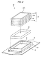
- the shield layer 27 has a platform 31 that is provided on the surface 28 and used for placing thereon the display device 30 and a wall part 32 provided upright around the platform 31 and surrounding the display device 30.
- the platform 31 is a flat surface having a rectangular shape.
- the wall part 32 is a rectangular frame.
- the platform 31 and the wall part 32 form a recessed part 34 housing the display device 30.
- the shield layer 27 is a layer formed by injecting a resin to which a metal filler is added.
- the resin has a dielectric constant of 3.6, and the silica filler (SiO 2 ) serving as the metal filler has a dielectric constant of 3 or less.
- the silica filler having an average particle diameter of 8 ⁇ m or more and a maximum particle diameter of 40 ⁇ m or less may preferably be used.
- the resin part 25 is provided with the reinforcing heat discharge layer 26 covering the electronic components 22 and the shield layer 27 covering the reinforcing heat discharge layer 26, a heat discharge property and a shield property for the electronic components are achieved.
- the surface 28 of the shield layer 27 has the predetermined shape corresponding to the surface shape of the display device 30. Therefore, it is possible to omit a support member, for example, that is used in the conventional examples, and, by forming the recessed part as required, it is possible to support the display device 30 in such a fashion that the display device is recessed as compared to the conventional examples.
- the recessed part 34 is formed by providing the platform 31 on the surface of the shield layer 27 and providing the wall part 32 upright around the platform 31.
- a reflection layer 33 is provided by adhesion.
- the reflection layer 33 is a white or silver sheet, for example, and is a frame-like sheet (or a sheet) having the shape of a rectangular frame. By using the white or silver sheet as the reflection layer 33, it is possible to increase reflection efficiency.
- the reflection layer 33 is the frame-like sheet, it is possible to simply attach the reflection layer by readily allowing the reflection layer 33 to follow the surface of the resin part 25.
- An LCD or the like may be used as the display device 30, and the display device 30 is disposed in such a fashion that a display surface 35A faces to an opening of the housing 12 and that an end face 35B faces to the reflection layer 33.
- a lower surface, i.e. a reflection sheet 38, of the display device 30 is placed on the platform 31.
- the display device 30 is obtained by laminating an optical sheet 36 on a lower surface of a main body 35, laminating a light guiding plate 37 on a lower surface of the optical sheet 36, and laminating the reflection sheet 38 on a lower surface of the light guiding plate 37.
- the main body 35 is obtained by providing a liquid crystal part (not shown) between a pair of transparent substrates 39.
- An electroconductive part 41 is provided on the transparent substrates 39, and a terminal 41A of the electroconductive part 41 is in contact with a top part 32A of the wall 32.
- a light guiding part (projection) 42 having a substantially wedge-like shape is formed at one end face of the light guiding plate 37.
- a light source (LED) 45 is so provided as to face the end face of the light guiding part 42.
- the light guiding part 42 Since the light guiding part 42 has the substantially wedge-like shape, the light guiding part 42 is projected toward a lower part of the light guiding plate 37.
- a recessed part 44 corresponding to the light guiding part 42 and the light source 45 is provided at a part of the platform 31 facing to the light guiding part 42 and the light source 45.
- a first die 47 is molded.
- a first cavity space 48 is formed.
- a melted resin for the reinforcing heat discharge layer 26 shown in Fig. 1 is injected into the first cavity space 48 from a gate 47A.
- the melted resin contains a filler for ensuring the heat discharge property and the reinforcing property.
- the first die 47 is opened.
- a second cavity space 52 is formed.
- a melted resin for the shield layer 27 shown in Fig. 1 is injected into the second cavity space 52 from a gate 51A.
- the melted resin contains a metal filler.
- the shield layer 27 is obtained.
- the second die 51 After the solidification of the melted resin, the second die 51 is opened. After opening the second die 51, the reflection layer 33 that is the frame-like sheet is attached along the inner surface of the wall part 32 as shown in Fig. 2 .
- the display device 30 After attaching the reflection layer 33, the display device 30 is housed in the recessed part 34 of the shield layer 27. When the reflection sheet 38 of the display device 30 is placed on the platform 31, the end face 35 of the display device 30 faces to the reflection layer 33.
- the reflection layer 33 may preferably be exposed from the inner surface of the wall part 32.
- the shield layer 27 of the first embodiment is replaced with a shield layer 61, and other parts of the structure are the same as those of the substrate structure 20 of the first embodiment.
- the shield layer 61 is obtained by attaching a wiring sheet to a surface 26A of the reinforcing heat discharge layer 26.
- the wiring sheet means the one obtained by wiring a plurality of linear conductors on a soft film, the one obtained by printing a linear conductor by meandering wiring, or the like.
- the conductor is provided for ensuring the shielding property.
- the wiring sheet As the shield layer 61, it is possible to reduce a thickness of the shield layer 61. Thus, it is possible to achieve further thinning of the substrate structure 60.
- the shield layer 61 is disposed between a die 62 and the electronic components 22.
- the shield layer 61 is disposed in such a manner that the shield layer 26 in the form of a roll is drawn to be placed between the die 62 and the electronic components 22,
- the shield layer 61 is attached to a molded surface 62A of the die 62 by vacuum contact, for example.
- the die is molded.
- a cavity space (not shown) is formed.
- a melded resin for the reinforcing heat discharge layer 26 shown in Fig. 7 is injected inside the cavity space from the gate 62B.
- the melted resin contains a filler for ensuring heat conductivity and a reinforcing property.
- the die 62 is opened.
- the wiring sheet as the shield layer 61 as described above, it is unnecessary to inject-mold the shield layer 61. Therefore, an equipment cost is suppressed since the use of only one set of the die 62 is sufficient.
- the reflection layer 33 shown in Fig. 2 is attached along the inner surface of the wall part 32.
- the display device 30 After attaching the reflection layer 33, the display device 30 is housed in the recessed part 34 of the shield layer 61.
- the reflection sheet 38 of the display device 30 When the reflection sheet 38 of the display device 30 is placed on the platform 31, the end face 35 of the display device 30 faces to the reflection layer 33 or the wall part 32.
- the substrate structure 60 of the second embodiment it is possible to reduce the number of the die 62 and to reduce the thickness of the substrate structure 60 by using the wiring sheet as the shield layer 61.
- the substrate structure 60 of the second embodiment it is possible to achieve the same effects as the substrate structure 20 of the first embodiment.
- a substrate structure 70 of the third embodiment shown in Figs, 10 and 11 is provided with a reflection layer 71 obtained by coating a white or silver coating matter, for example, on the inner surface of the wall part 32, and other parts of the structure are the same as those of the substrate structure 20 of the first embodiment.
- reflection efficiency is improved. Since the reflection efficiency is improved by of the reflection layer 71 as described above, it is possible to obtain a high-brightness display device reduced in light loss.
- the substrate structure 70 of the third embodiment by using the coating matter as the reflection layer 71, it is possible to reduce the number of components since it is unnecessary to use the frame-like sheet as the reflection layer 33 as in the first embodiment.
- the substrate structure 70 of the third embodiment it is possible to achieve the same effects as the substrate structure 20 of the first embodiment.
- a substrate structure 80 of the fourth embodiment shown in Figs. 12 and 13 is provided with a reflection layer 81 obtained by coating a white or silver coating matter, for example, on the end face of the display device 30, and other parts of the structure are the same as those of the substrate structure 20 of the first embodiment.
- reflection efficiency is improved. Since the reflection efficiency is improved by the reflection layer 81 as described above, it is possible to obtain a high-brightness display device reduced in light loss.
- the substrate structure 80 of the fourth embodiment by using the coating matter as the reflection layer 81, it is possible to reduce the number of components since it is unnecessary to use the frame-like sheet as the reflection layer 33 as in the first embodiment.
- the reflection layer 81 on the end face 35B of the display device 30, it is possible to coat the display device 30 before incorporating the display device 30 into the recessed part 34 of the shield layer 27.
- the substrate structure 70 of the third embodiment it is possible to achieve the same effects as the substrate structure 20 of the first embodiment.
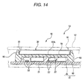
- the mobile terminal 10 shown in Fig. 14 has a substrate structure 90 of the fifth embodiment in the inner space 14 of the housing 12.
- the substrate structure 90 of the fifth embodiment is provided with the substrate 21, the plurality of electronic components 22 mounted along the substrate 21, and a resin part 91 covering the electronic components 22 and in close contact with the substrate 21.
- the resin part 91 is provided with a reinforcing heat discharge layer 26 covering the electronic components 22 and having heat conductivity and a reinforcing property and a shield layer 92 covering the reinforcing heat discharge layer 26,
- the shield layer 92 is replaced with the shield layer 27 of the first embodiment, and other parts of the structure are the same as those of the first embodiment.
- the shield layer 92 is obtained by inserting a metal sheet (metal plate) 94 into a resin layer 93 to ensure the shielding property.
- the metal sheet 94 is used as the shield material in the substrate structure 90 of the fifth embodiment, it is unnecessary to add a metal filler as in the shield layer 27 (see Fig. 1 ) of the first embodiment.
- the resin to be used for injection-molding the shield layer 92 is more easily obtained.
- the metal sheet 94 is exposed to a surface 93A of the resin layer 93.
- a platform for placing thereon the display device 30 is formed by the metal sheet 94.
- the metal sheet is used also as a reflection layer of the display device 30.
- the reflection layer 33 is provided on the inner surface of a wall part 96 of the resin layer 94 as in the first embodiment.
- the substrate structure 90 of the fifth embodiment it is possible to achieve the thinning and the reduction in number of components of the mobile terminal 10 by inserting the metal sheet 94 into the shield layer 92.
- the substrate structure 90 of the fifth embodiment it is possible to achieve the same effects as the substrate structure 20 of the first embodiment.
- a wiring sheet may be used in place of the metal sheet 94. This wiring sheet is the same as that used in the second embodiment.
- the wiring sheet means the one obtained by wiring a plurality of linear conductors on a soft film, the one obtained by printing a linear conductor by meandering wiring, or the like.
- the conductor is provided for ensuring the shielding property.
- a platform 101 serves as an inclined surface 37A of the light guiding plate 37 of the display device 30, and electronic components 22 having a large mounting height among the electronic components 22 are disposed at an upstream of an inclination direction of the platform 101.
- Other parts of the structure are the same as those of the substrate structure 20 of the first embodiment.
- the platform 101 as the inclined surface 37A of the light guiding plate 37 of the display device 30, it is possible to reflect light made incident from an end face 42A of the light guiding part 42 provided on the light guiding plate 37 by the inclined surface 37A to cause the light to uniformly exit from a surface 37B of the light guiding plate 37, thereby obtaining a high-brightness display device reduced in irregularity.
- the substrate structure 100 of the sixth embodiment since the electronic components 22 having a large mounting height among the electronic components 22 are disposed at an upstream of an inclination direction of the platform 01, it is possible dispose the platform 101 closer to the substrate 21 as well as to avoid constricting downsizing and thinning of the mobile terminal 10.
- the substrate structure 100 of the sixth embodiment it is possible to achieve the same effects as the substrate structure 20 of the first embodiment.
- a substrate structure 110 of the seventh embodiment is provided with the substrate 21, the plurality of electronic components 22 mounted along the substrate 21, and a resin part 111 covering the electronic components 22 and in close contact with the substrate 21.
- the resin part 111 is a resin member having high heat conductivity and reinforcing property, and examples thereof include those obtainable by adding silica (SiO 2 ), alumina (AlO 2 ), silicon carbide (SiC), AIN, carbon (C), or general electro-conductive fillers such as Cu, Au, AG, and Ni to an epoxy-based resin.
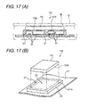
- the display device 30 that is one of the components is deposed on the resin part 111.
- the resin part 111 has an upper surface 111A having a rectangular shape having an area S1.
- the display device 30 has a lower surface 30A having a rectangular shape having an area S2.
- a relationship between the area S1 and the area S2 is S1>S2.
- the display device 30 which is the component disposed on the resin part 111 is disposed in such a fashion that the planar outline of the display device 30 is prevented from deviating from the planar outline of the resin part 111, damage is hardly or never caused on the display device 30, resin part 111, and the like when a load is applied on the display device 30, thereby making it possible to improve strength as compared to the conventional examples.
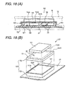
- a substrate structure 120 of the eighth embodiment is provided with the substrate 21, the plurality of electronic components 22 mounted along the substrate 21, a resin part 121 covering the electronic components 22 and in close contact with the substrate 21, and a frame 122 covering the resin part 121.
- the resin part 121 is, like the resin part 111 of the seventh embodiment, a resin member having high heat conductivity and reinforcing property, and examples thereof include those obtainable by adding silica (SiO 2 ), alumina (AlO 2 ), silicon carbide (SiC), AIN, carbon (C), or general electro-conductive fillers such as Cu, Au, AG, and Ni to an epoxy-based resin.
- the frame 122 is formed of a metal frame 123 provided around the resin part 121 and a metal cover 124 covered on the metal frame 123 and serves as a shielding material.
- the display device 30 that is one of the components is deposed on the metal cover 124 of the frame 122.
- the metal cover 124 has an upper surface 124A having a rectangular shape having an area S1.
- the display device 30 has a lower surface 30A having a rectangular shape having an area S2.
- a relationship between the area S1 and the area S2 is S1 >S2.
- the display device 30 is disposed in such a fashion that the planar outline of the display device 30 is prevented from deviating from the planar outline of the upper surface 124A, damage is hardly or never caused on the display device 30, resin part 121, and the like when a load is applied on the display device 30, thereby making it possible to improve strength as compared to the conventional examples.
- the display device 30 is disposed on an upper surface 121 A of the resin part 121.
- an upper rim 123A of the metal frame 123 and the upper surface 121 A of the resin part 121 are aligned along an identical a plane, and the display device 30 is disposed on the upper rim 123A and the upper surface 121A.
- the display device 30 is disposed on an upper rim 123A of the metal frame 123.
- the shapes and the sizes of the reinforcing heat discharge layer 26, the shield layer 27, and the display device 30 described in the first to the sixth embodiments may be changed as required.
- the display device 30 is described as another member in the first to the sixth embodiments, the another member is not limited to the display device 30, and members other than the display device may be used as the another member.
- the display device 30 is described as one of the components in the seventh and eighth embodiments, a keyboard, touch panel, a storage cell, and the like may be used as the one of the components.
- This invention is suitably applied to substrate structures wherein: plural electronic components are disposed along a substrate; the electronic components are covered with a resin part; and the resin part is in close contact with the substrate.
Landscapes
- Engineering & Computer Science (AREA)
- Microelectronics & Electronic Packaging (AREA)
- Physics & Mathematics (AREA)
- Manufacturing & Machinery (AREA)
- Electromagnetism (AREA)
- Thermal Sciences (AREA)
- Devices For Indicating Variable Information By Combining Individual Elements (AREA)
- Structure Of Printed Boards (AREA)
- Non-Metallic Protective Coatings For Printed Circuits (AREA)
- Shielding Devices Or Components To Electric Or Magnetic Fields (AREA)
- Liquid Crystal (AREA)
Applications Claiming Priority (2)
| Application Number | Priority Date | Filing Date | Title |
|---|---|---|---|
| JP2005250200 | 2005-08-30 | ||
| PCT/JP2006/302969 WO2007026439A1 (fr) | 2005-08-30 | 2006-02-20 | Structure de substrat |
Publications (2)
| Publication Number | Publication Date |
|---|---|
| EP1933609A1 true EP1933609A1 (fr) | 2008-06-18 |
| EP1933609A4 EP1933609A4 (fr) | 2011-01-05 |
Family
ID=37808543
Family Applications (1)
| Application Number | Title | Priority Date | Filing Date |
|---|---|---|---|
| EP06714109A Withdrawn EP1933609A4 (fr) | 2005-08-30 | 2006-02-20 | Structure de substrat |
Country Status (6)
| Country | Link |
|---|---|
| US (1) | US7969741B2 (fr) |
| EP (1) | EP1933609A4 (fr) |
| JP (1) | JP4795355B2 (fr) |
| KR (1) | KR20080039507A (fr) |
| CN (1) | CN101273674A (fr) |
| WO (1) | WO2007026439A1 (fr) |
Cited By (3)
| Publication number | Priority date | Publication date | Assignee | Title |
|---|---|---|---|---|
| EP2704536A1 (fr) * | 2012-08-31 | 2014-03-05 | Harman Becker Automotive Systems GmbH | Procédé de production d'un système de carte de circuit imprimé |
| CN103633069A (zh) * | 2012-08-24 | 2014-03-12 | 富士通株式会社 | 封装结构和电子设备 |
| US10492347B2 (en) | 2013-07-05 | 2019-11-26 | Bayerische Motoren Werke Aktiengesellschaft | Method for producing a housing having shielding against electric and/or magnetic radiation, and housing having the shielding |
Families Citing this family (19)
| Publication number | Priority date | Publication date | Assignee | Title |
|---|---|---|---|---|
| JP5504683B2 (ja) * | 2009-04-27 | 2014-05-28 | セイコーエプソン株式会社 | 電気光学装置及び電子機器 |
| WO2011007570A1 (fr) * | 2009-07-17 | 2011-01-20 | パナソニック株式会社 | Module électronique et procédé de fabrication de celui-ci |
| JP2011054640A (ja) * | 2009-08-31 | 2011-03-17 | Funai Electric Co Ltd | シールドパッケージ基板 |
| US8988628B2 (en) * | 2011-06-23 | 2015-03-24 | Apple Inc. | Coated chassis for liquid crystal display |
| JP6035015B2 (ja) * | 2011-09-09 | 2016-11-30 | ソニー株式会社 | 回路基板 |
| US9244215B2 (en) * | 2011-09-09 | 2016-01-26 | Apple Inc. | Chassis for display backlight |
| KR101450950B1 (ko) * | 2011-10-04 | 2014-10-16 | 엘지디스플레이 주식회사 | 드라이버 패키지 |
| TWI528149B (zh) * | 2011-12-14 | 2016-04-01 | 英特爾股份有限公司 | 具有熱解決方案之裝置及具有熱解決方案之方法 |
| US9247034B2 (en) * | 2013-08-22 | 2016-01-26 | Asia Vital Components Co., Ltd. | Heat dissipation structure and handheld electronic device with the heat dissipation structure |
| US9576930B2 (en) * | 2013-11-08 | 2017-02-21 | Taiwan Semiconductor Manufacturing Co., Ltd. | Thermally conductive structure for heat dissipation in semiconductor packages |
| TW201524284A (zh) * | 2013-12-03 | 2015-06-16 | Toyo Ink Sc Holdings Co Ltd | 電子元件以及片材 |
| ES2724914T3 (es) * | 2013-12-25 | 2019-09-17 | Kyocera Corp | Dispositivo electrónico |
| KR102488830B1 (ko) * | 2015-12-14 | 2023-01-13 | 에이.케이 스탬핑 컴퍼니, 인크. | 멀티 피스 실드 |
| EP4325264A3 (fr) * | 2016-04-13 | 2024-05-22 | TactoTek Oy | Structure multicouche éclairée avec sources de lumière intégrées |
| JP2018098927A (ja) * | 2016-12-14 | 2018-06-21 | 株式会社オートネットワーク技術研究所 | 電気接続箱 |
| US10802198B1 (en) * | 2019-03-29 | 2020-10-13 | Dura Operating, Llc | Structural support elements of light guide and electrical housing |
| US11089673B2 (en) * | 2019-07-19 | 2021-08-10 | Raytheon Company | Wall for isolation enhancement |
| US12213242B2 (en) * | 2021-06-24 | 2025-01-28 | Samsung Electronics Co., Ltd. | Electronic device including a structure for guiding an arrangement position of an electronic component |
| WO2022270988A1 (fr) * | 2021-06-24 | 2022-12-29 | 삼성전자 주식회사 | Dispositif électronique comprenant une structure pour guider des emplacements d'agencement de composants électroniques |
Family Cites Families (15)
| Publication number | Priority date | Publication date | Assignee | Title |
|---|---|---|---|---|
| JPH03241669A (ja) | 1990-02-20 | 1991-10-28 | Yuasa Battery Co Ltd | 非水溶液電池とその集合電池 |
| JPH10104584A (ja) * | 1996-09-27 | 1998-04-24 | Kyocera Corp | 液晶表示装置 |
| US5991155A (en) * | 1996-12-13 | 1999-11-23 | Mitsubishi Denki Kabushiki Kaisha | Heat sink assembly including flexible heat spreader sheet |
| JP3241669B2 (ja) | 1998-11-09 | 2001-12-25 | 埼玉日本電気株式会社 | Icパッケージの補強構造 |
| JP3387439B2 (ja) * | 1999-03-12 | 2003-03-17 | 松下電器産業株式会社 | 面照明装置及びこの面照明装置を用いた表示装置及びこの表示装置を用いた携帯機器 |
| US7088333B1 (en) | 1999-03-12 | 2006-08-08 | Matsushita Electric Industrial Co., Ltd. | Surface lighting device and portable terminal using the same |
| JP2001024312A (ja) | 1999-07-13 | 2001-01-26 | Taiyo Yuden Co Ltd | 電子装置の製造方法及び電子装置並びに樹脂充填方法 |
| US20010019379A1 (en) * | 2000-01-31 | 2001-09-06 | Takayuki Ishihara | Front light type liquid crystal display |
| KR100784804B1 (ko) | 2001-05-07 | 2007-12-14 | 삼성전자주식회사 | 액정 표시 장치 및 제조 방법 |
| JP2004031651A (ja) * | 2002-06-26 | 2004-01-29 | Sony Corp | 素子実装基板及びその製造方法 |
| US6940712B2 (en) * | 2002-07-17 | 2005-09-06 | International Business Machines Corporation | Electronic device substrate assembly with multilayer impermeable barrier and method of making |
| KR100756147B1 (ko) * | 2003-03-31 | 2007-09-05 | 산요 일렉트릭 컴퍼니 리미티드 | 액정 표시 장치 |
| TW585342U (en) * | 2003-04-25 | 2004-04-21 | Cateron Corp | Composite material structure with high heat conduction and electromagnetic shielding functions |
| US7292441B2 (en) * | 2003-11-25 | 2007-11-06 | Advanced Energy Technology Inc. | Thermal solution for portable electronic devices |
| US7760290B2 (en) * | 2005-04-08 | 2010-07-20 | Bong Sup Kang | Multi-reflecting device and backlight unit and display device having multi-reflecting architecture |
-
2006
- 2006-02-20 EP EP06714109A patent/EP1933609A4/fr not_active Withdrawn
- 2006-02-20 CN CNA2006800353346A patent/CN101273674A/zh active Pending
- 2006-02-20 US US12/065,177 patent/US7969741B2/en not_active Expired - Fee Related
- 2006-02-20 JP JP2007533117A patent/JP4795355B2/ja not_active Expired - Fee Related
- 2006-02-20 WO PCT/JP2006/302969 patent/WO2007026439A1/fr not_active Ceased
- 2006-02-20 KR KR1020087007028A patent/KR20080039507A/ko not_active Ceased
Cited By (5)
| Publication number | Priority date | Publication date | Assignee | Title |
|---|---|---|---|---|
| CN103633069A (zh) * | 2012-08-24 | 2014-03-12 | 富士通株式会社 | 封装结构和电子设备 |
| EP2704536A1 (fr) * | 2012-08-31 | 2014-03-05 | Harman Becker Automotive Systems GmbH | Procédé de production d'un système de carte de circuit imprimé |
| US9706637B2 (en) | 2012-08-31 | 2017-07-11 | Harman Becker Automotive Systems Gmbh | Method for producing a circuit board system |
| US10492347B2 (en) | 2013-07-05 | 2019-11-26 | Bayerische Motoren Werke Aktiengesellschaft | Method for producing a housing having shielding against electric and/or magnetic radiation, and housing having the shielding |
| EP3016799B1 (fr) * | 2013-07-05 | 2020-05-20 | Bayerische Motoren Werke Aktiengesellschaft | Procédé de fabrication d'un boîtier équipé d'un blindage anti-rayonnement électrique et/ou magnétique et boîtier équipé d'un blindage anti-rayonnement électrique et/ou magnétique |
Also Published As
| Publication number | Publication date |
|---|---|
| CN101273674A (zh) | 2008-09-24 |
| JP4795355B2 (ja) | 2011-10-19 |
| EP1933609A4 (fr) | 2011-01-05 |
| US20100020497A1 (en) | 2010-01-28 |
| KR20080039507A (ko) | 2008-05-07 |
| JPWO2007026439A1 (ja) | 2009-03-26 |
| US7969741B2 (en) | 2011-06-28 |
| WO2007026439A1 (fr) | 2007-03-08 |
Similar Documents
| Publication | Publication Date | Title |
|---|---|---|
| US7969741B2 (en) | Substrate structure | |
| KR101884628B1 (ko) | 발광 모듈 및 백라이트 유닛 | |
| US9112125B2 (en) | Light emitting device, method of fabricating the same and lighting system having the same | |
| JP5304431B2 (ja) | リードフレーム及びその製造方法及びそれを用いた半導体発光装置 | |
| US8446557B2 (en) | Liquid crystal display device | |
| CN114677910B (zh) | 显示装置和显示设备 | |
| US12557228B2 (en) | Display module and display device with attached coverplate | |
| JP2011205100A (ja) | 発光素子パッケージ及びこれを備えた照明システム | |
| US8568861B2 (en) | Metallic laminate and manufacturing method of light emitting diode package using the same | |
| US9400349B2 (en) | Electronic device with display chassis structures | |
| CN101640973A (zh) | 电子设备、柔性印刷线路板以及制造柔性印刷线路板的方法 | |
| EP2365552A2 (fr) | Boitier d'un dispositif électroluminescent avec une grille de connexion ayant une cavité | |
| US6049094A (en) | Low stress package assembly for silicon-backed light valves | |
| CN117877386A (zh) | 一种显示模组及显示装置 | |
| CN115985197B (zh) | 一种显示模组、显示装置及其制作方法、注塑模具 | |
| US11467437B2 (en) | Electronic device | |
| KR101189401B1 (ko) | 연성 회로기판 및 그의 제조 방법 | |
| KR101873586B1 (ko) | 표시장치 | |
| KR102063519B1 (ko) | 인쇄회로기판 및 이를 갖는 광원 모듈 | |
| KR20130079921A (ko) | 인쇄 회로 기판 | |
| JP2007142085A (ja) | 発光装置、及び発光装置の製造方法 | |
| KR20080018718A (ko) | 액정 표시 장치 | |
| KR101093428B1 (ko) | 액정표시장치 램프 홀더 및 그 제조방법 | |
| CN119694212A (zh) | 显示模组及显示装置 | |
| CN117082927A (zh) | 一种显示装置及其制作方法及电子设备 |
Legal Events
| Date | Code | Title | Description |
|---|---|---|---|
| PUAI | Public reference made under article 153(3) epc to a published international application that has entered the european phase |
Free format text: ORIGINAL CODE: 0009012 |
|
| 17P | Request for examination filed |
Effective date: 20080328 |
|
| AK | Designated contracting states |
Kind code of ref document: A1 Designated state(s): DE FR GB |
|
| RBV | Designated contracting states (corrected) |
Designated state(s): DE FR GB |
|
| RAP1 | Party data changed (applicant data changed or rights of an application transferred) |
Owner name: PANASONIC CORPORATION |
|
| A4 | Supplementary search report drawn up and despatched |
Effective date: 20101206 |
|
| 17Q | First examination report despatched |
Effective date: 20110720 |
|
| STAA | Information on the status of an ep patent application or granted ep patent |
Free format text: STATUS: THE APPLICATION IS DEEMED TO BE WITHDRAWN |
|
| 18D | Application deemed to be withdrawn |
Effective date: 20111201 |