EP1936478A2 - Dispositif de détection de position - Google Patents
Dispositif de détection de position Download PDFInfo
- Publication number
- EP1936478A2 EP1936478A2 EP07011905A EP07011905A EP1936478A2 EP 1936478 A2 EP1936478 A2 EP 1936478A2 EP 07011905 A EP07011905 A EP 07011905A EP 07011905 A EP07011905 A EP 07011905A EP 1936478 A2 EP1936478 A2 EP 1936478A2
- Authority
- EP
- European Patent Office
- Prior art keywords
- light
- guide plate
- coordinate
- unit
- position detecting
- Prior art date
- Legal status (The legal status is an assumption and is not a legal conclusion. Google has not performed a legal analysis and makes no representation as to the accuracy of the status listed.)
- Granted
Links
Images


Classifications
-
- G—PHYSICS
- G06—COMPUTING OR CALCULATING; COUNTING
- G06F—ELECTRIC DIGITAL DATA PROCESSING
- G06F3/00—Input arrangements for transferring data to be processed into a form capable of being handled by the computer; Output arrangements for transferring data from processing unit to output unit, e.g. interface arrangements
- G06F3/01—Input arrangements or combined input and output arrangements for interaction between user and computer
- G06F3/03—Arrangements for converting the position or the displacement of a member into a coded form
- G06F3/041—Digitisers, e.g. for touch screens or touch pads, characterised by the transducing means
- G06F3/042—Digitisers, e.g. for touch screens or touch pads, characterised by the transducing means by opto-electronic means
- G06F3/0421—Digitisers, e.g. for touch screens or touch pads, characterised by the transducing means by opto-electronic means by interrupting or reflecting a light beam, e.g. optical touch-screen
-
- G—PHYSICS
- G06—COMPUTING OR CALCULATING; COUNTING
- G06F—ELECTRIC DIGITAL DATA PROCESSING
- G06F3/00—Input arrangements for transferring data to be processed into a form capable of being handled by the computer; Output arrangements for transferring data from processing unit to output unit, e.g. interface arrangements
- G06F3/01—Input arrangements or combined input and output arrangements for interaction between user and computer
- G06F3/03—Arrangements for converting the position or the displacement of a member into a coded form
- G06F3/033—Pointing devices displaced or positioned by the user, e.g. mice, trackballs, pens or joysticks; Accessories therefor
- G06F3/0354—Pointing devices displaced or positioned by the user, e.g. mice, trackballs, pens or joysticks; Accessories therefor with detection of two-dimensional [2D] relative movements between the device, or an operating part thereof, and a plane or surface, e.g. 2D mice, trackballs, pens or pucks
- G06F3/03542—Light pens for emitting or receiving light
-
- G—PHYSICS
- G06—COMPUTING OR CALCULATING; COUNTING
- G06F—ELECTRIC DIGITAL DATA PROCESSING
- G06F3/00—Input arrangements for transferring data to be processed into a form capable of being handled by the computer; Output arrangements for transferring data from processing unit to output unit, e.g. interface arrangements
- G06F3/01—Input arrangements or combined input and output arrangements for interaction between user and computer
- G06F3/03—Arrangements for converting the position or the displacement of a member into a coded form
- G06F3/033—Pointing devices displaced or positioned by the user, e.g. mice, trackballs, pens or joysticks; Accessories therefor
- G06F3/038—Control and interface arrangements therefor, e.g. drivers or device-embedded control circuitry
- G06F3/0386—Control and interface arrangements therefor, e.g. drivers or device-embedded control circuitry for light pen
-
- G—PHYSICS
- G06—COMPUTING OR CALCULATING; COUNTING
- G06F—ELECTRIC DIGITAL DATA PROCESSING
- G06F2203/00—Indexing scheme relating to G06F3/00 - G06F3/048
- G06F2203/041—Indexing scheme relating to G06F3/041 - G06F3/045
- G06F2203/04109—FTIR in optical digitiser, i.e. touch detection by frustrating the total internal reflection within an optical waveguide due to changes of optical properties or deformation at the touch location
Definitions
- the present invention relates to position detecting devices that optically detect positions indicated by the indicating units upon an image display screen.
- a touch panel As a device that optically detects a position indicated by an indicating unit upon an image display screen, a touch panel (touchscreen) is proposed in which, an illumination means is provided on one side of mutually opposing sides of a light-guide plate made of a translucent material and placed upon a displaying surface (screen) of a displaying device, and a light-sensor array is provided on the other side thereof; an indicating unit (input pen or stylus) that has a contacting part made of a translucent material at the unit's tip is contacted with the top surface of the light-guide plate; thereby, a position of the indicating unit is detected according to the change in the amount of light that reaches the light-sensor array (for example, refer to Patent Publication 1).
- an illumination means is provided on one side of mutually opposing sides of a light-guide plate made of a translucent material and placed upon a displaying surface (screen) of a displaying device, and a light-sensor array is provided on the other side thereof; an indicating unit (
- Patent Publication 1 Japanese Patent Application Publication No. H12-172444 (2000 ), paragraphs 0017 through 0034, Fig. 1 .
- a position of the indicating unit is detected by adjusting the light emitted from the illumination means so as to be directed toward the opposing side of the light-guide plate, as being totally reflected thickness-wise, and by detecting a decrease of the amount of light that reaches the light-sensor array opposed to the illumination means, due to disturbance in conditions for the total reflection, caused by the indicating unit in contact with the plate.
- the present invention has been directed at solving these problems with the conventional technologies described above, and an object of the invention is to provide a position detecting device that is able to accurately detect an indicated position via an indicating unit or device even when a water droplet or the like is formed upon the position-detecting-device's surface.
- a position detecting device comprises: a light-guide plate for placement upon a displaying surface of a displaying device, and made of a translucent material; an emitting unit for emitting, from the sides of the light-guide plate, arranged in line along the X-axis and the Y-axis, a plurality of light beams each of a predetermined width, so as to be totally reflected thickness-wise within the light-guide plate and to travel heading in predetermined directions parallel to the light-guide-plate plane; an emission-control unit for controlling the emitting unit so as to make the light beams each scan the light-guide plate in progression along the sides thereof, in an X-axis direction and in a Y-axis direction; at least one indicating device having a light-guiding part for guiding, by contacting the light-guide plate, thereinto light traveling within the light-guide plate, and a detection unit for outputting, by detecting the light guided via the light-guiding part, a detection signal; and a coordinate calculating
- Fig. 1(a) through Fig. 4(b) are diagrams showing a position detecting device in Embodiment 1 of the present invention, that is placed upon the image display screen of a displaying device.
- Fig. 1(a) is a top plan diagram outlining a configuration of the position detecting device, and Fig. 1(b) is a cross-sectional side diagram thereof (viewed from the bottom);
- Fig. 2 is a diagram outlining a configuration of an indicating device of the position detecting device;
- Fig. 3 is a block diagram outlining part of a circuit of the position detecting device;
- Fig. 4(a) is a diagram outlining an emission-control pattern, and Fig.
- the position detecting device has a light-guide plate 1 that is a square-shaped flat plate made of a transparent or translucent material; an emitting unit 2 that emits, from sides of the light-guide plate 1, arranged in line, a plurality of light beams each of a predetermined width, so as to be totally reflected thickness-wise within the light-guide plate 1 and to travel heading in predetermined directions parallel to the plane of the light-guide plate 1; an emission-control unit 3 that controls an emission pattern for the emitting unit 2 so that the light beams emitted from the emitting unit 2 scan the light-guide plate 1 in progression along the sides thereof; and at least one indicating device 4.
- the light-guide plate 1 is a square-shaped glass plate having a refractive index of some 1.5 and a the thickness of some 5 mm, and is placed with a gap upon the displaying surface (screen) of the displaying device not shown in the figures; it is possible to watch the screen of the displaying device through the light-guide plate 1.
- the emitting unit 2 has a plurality of light sources 21 (19 light sources along the X-axis, and 13 light sources along the Y-axis), and optical processing units 22 that, corresponding to the light sources 21 each, form light outputted from the light sources 21 into light beams, and emit the light beams each, arranged in line, from the sides of the light-guide plate 1.
- the light sources 21 used are infrared semiconductor lasers that have two-dimensionally-spreading characteristics in their output distribution.
- Infrared semiconductor lasers are characterized in that the output distribution of the light outputted from the light sources 21 each two-dimensionally spreads; however, the outputted light is shaped by collimating lenses and cylindrical lenses that constitute the optical processing units 22, is diffused thickness-wise in the light-guide plate 1 within a predetermined angle, and in the light-guide-plate plane, is formed into light beams, each of which is parallel to the sides adjoining to each opposing (other) side, and is several millimeters (mm) in width.
- the shaped light (light beams each) is thus emitted toward the opposing sides of the light-guide plate 1 for the light sources 21 each, and, as shown in Fig.
- the emitting unit 2 is constructed of an emitting unit 2x that is placed on the top side 1u of the light-guide plate 1, so as to allow laterally (along the X-axis) 19 light beams to be arranged in line, and of an emitting unit 2y that is placed on the right side 1r of the light-guide plate 1, so as to allow vertically (along the Y-axis) 13 light beams to be arranged in line.
- the light beams emitted from the emitting unit 2x travel inside the light-guide plate 1 keeping parallelism to the right side 1r that perpendicularly adjoins to the emitted top side 1u, so as to reach the bottom side 1d; the light beams emitted from the emitting unit 2y travel inside the light-guide plate 1 keeping parallelism to the top side 1u that perpendicularly adjoins to the emitted right side 1r, so as to reach the left side 1L.
- adjoining optical paths of the light beams so as to mutually overlap inside the light-guide plate 1, it is possible to eliminate areas where the light beams do not travel.
- the emission-control unit 3 is constructed of laser drivers 3a that drive the light sources 21 each, and a control unit 3b that controls the laser drivers 3a each; the emission-control unit 3 is dedicated to control the light sources 21 each to be powered on/off so that the light beams each emitted from the emitting unit 2 scan the light-guide plate 1 progressively along the sides (lu and lr) thereof at some 10 ms intervals.
- the indicating device 4 has a light-guiding part 41 that guides, by contacting the light-guide plate 1, thereinto light traveling within the light-guide plate 1; a detection unit 42 that outputs, by detecting the light guided via the light-guiding part 41, a detection signal; and further, a coordinate calculating unit 43 that calculates, based on a scanned position derived from the detection signal and the emission-control unit 3, a coordinate position where the indicating device 4 contacts the light-guide plate 1.
- the structure of the indicating device 4 will be explained based on Fig. 2 .
- two of such indicating devices 4 are used; in order to designate individually each of them, "A” or “B” is affixed to the numeral "4" such as an "indicating device 4A” or an “indicating device 4B,” and when referred to as a whole, they are designated the "indicating device 4."
- the light-guiding part 41 made of a transparent resin of high flexibility is provided.
- the light-guiding part 41 has a refractive index that is approximately the same as that of the light-guide plate 1; when the light-guiding part 41 is pressed upon the light-guide plate 1 with a predetermined pressure, it is closely contacted with the light-guide plate 1 to become optically joined with the light-guide plate 1 as if one part, so that, while disturbing conditions for the total reflection within the light-guide plate 1, the light-guiding part 41 guides light traveling in the light-guide plate 1 into the inside thereof.
- the guided light is detected by the detection unit 42 inside the indicating device 4, and is converted into an electric signal so as to be outputted as a detection signal.
- the indicating device 4 has the coordinate calculating unit 43 that, based on the detection signal outputted from the detection unit 42 and a timing of scanning by the emission-control unit 3, determines that which light beam from the light sources the light detected by the light-guiding part 41 stems from, and outputs a coordinate signal SC after having calculated the coordinate position where the indicating device 4 contacts the light-guide plate 1.
- different identification information is assigned to the indicating device 4A and the indicating device 4B, and each of them has an identification-signal outputting unit 44 that outputs after having generated an identification signal SI based on the different identification information.
- the coordinate signal SC and the identification signal SI are outputted into a transmitting unit 45 whose transmitting frequency is in a band of 2.4 GHz, and together with the identification signal SI, the coordinate signal SC is externally transmitted from the transmitting unit 45 as a transmitting signal ST.
- the transmitting signal ST transmitted from the transmitting unit 45 of the indicating device 4 is received by a coordinate outputting device 5.
- the coordinate outputting device 5 has, as shown in Fig. 3 , a receiving unit 51 that receives the transmitting signal ST from the indicating device 4, and a central processing unit (CPU) 52 that separates the transmitting signal ST received by the receiving unit 51 into the coordinate signal SC and the identification signal SI, and outputs the coordinate position of the indicating device 4. And then, an output from the CPU 52 of the coordinate outputting device 5 is outputted into a computer 62 via an external interface 61 such as a local-area network (LAN) and a universal serial bus (USB).
- LAN local-area network
- USB universal serial bus
- the computer 62 application software has been installed thereinside; thereby, based on the coordinate positions outputted for each of the indicating devices 4A and 4B, images to be displayed onto a displaying surface (screen), not shown in the figures, are controlled so that the images controlled based on the position information of the indicating device 4A and the indicating device 4B are outputted on the displaying surface (screen); thus, it is possible to watch the images through the light-guide plate 1.
- the receiving unit 51 has two of such receiving units 51A and 51B corresponding to the indicating devices 4A and 4B, respectively.
- the emission-control unit 3 repeatedly performs an emission control in some 10 ms per one cycle that includes, as shown in Fig. 4(a) , after a first simultaneous control WL1 that totally powers on and off the light sources 21 twice in predetermined time-intervals, scanning-type controls SL that perform to power on nineteen light sources in the emitting unit 2x of the light sources 21 so as to make the light beams each scan in progression from left to right along the sides of the light-guide plate 1 (progressive scanning SLX) and, next, to power on thirteen light sources in the emitting unit 2y of the light sources 21 so as to make the light beams each scan in progression from bottom to top along the sides of the light-guide plate 1 (progressive scanning SLY), and a second simultaneous control WL2 that totally powers on the light sources 21 once again for a predetermined time.
- scanning-type controls SL that perform to power on nineteen light sources in the emitting unit 2x of the light sources 21 so as to make the light beams each scan in progression from left to right
- Light outputted from the light sources 21 each is shaped in the optical processing units 22, and is emitted as light beams each of a predetermined width; the emitted light beams travel, as described above, so as to be totally reflected thickness-wise within the light-guide plate 1, in a state parallel to the sides adjoining to each emitted side thereof, heading toward the opposing (other) sides thereof.
- the detection unit 42A when the indicating device 4A is placed at a position (3, 10) in Fig. 1(a) , a signal the detection unit 42A outputs becomes as shown in Fig. 4(b) . In whichever areas the indicating device 4A is placed upon the light-guide plate 1, the detection unit 42A detects part of light beams when the light sources 21 are totally powered on by the first simultaneous control WL1, and outputs a first signal S1.
- the indicating device 4A is contacting the light-guide plate 1
- a third light beam from the left in the emitting unit 2x of the light sources 21 is detected, and an X-scanned signal Sx is outputted;
- a tenth light beam from the bottom in the emitting unit 2y of the light sources 21 is detected, and a Y-scanned signal Sy is outputted; and finally, part of light beams are detected when the light sources 21 are totally powered on for a predetermined time by the second simultaneous control WL2, and a second signal S2 is outputted.
- the amount of light that is guided into the light-guiding part 41 is small in comparison to that of the light beams; thereby, even when a plurality of such indicating devices 4 is used, other such indicating devices 4 do not exert an effect on a position detecting accuracy thereof.
- a water droplet is formed on the surface of the light-guide plate 1 that is the topmost surface of the image display screen, and hence, part of the light escapes out of the light-guide plate 1, the amount of light reaching the opposing sides decreases to a small extent; thus, there does not exist a problem in that a position of the water droplet is erroneously recognized as the position of the indicating device 4.
- the first signal S1 can be distinguished from other signals by powering on and off twice in predetermined time-intervals in the first simultaneous control WL1 as described above; similarly, the second signal S2 can also be distinguished from other signals by powering on for a predetermined time in the second simultaneous control WL2.
- a time the light beams each are emitted according to the scanning that is controlled by the emission-control unit 3 can be easily calculate based on the time from the first simultaneous control WL1 to the second simultaneous control WL2, by distinguishing the first signal S1 and the second signal S2 from the X-scanned signal Sx and the Y-scanned signal Sy, it is possible to identify the light sources 21 of which the light beams are detected.
- the light beams each emitted from the emitting unit 2x travel parallel to the Y-axis while keeping a predetermined width
- the light beams each emitted from the emitting unit 2y also travel parallel to the X-axis while keeping a predetermined width
- a coordinate calculating unit 43A of the indicating device 4A identifies, based on the detection signal outputted from the detection unit 42A, the detected light beams whether the light beams are from which of the light sources 21 stemmed; in addition, based on the light sources 21 having been identified, it is possible to calculate a two-dimensional coordinate position of the indicating device 4A upon the light-guide plate 1. What is more, because the emission control constitutes a short time of some 10 ms per one cycle to some extent, it is possible to smoothly detect in real time a position of the indicating device 4A in motion.
- two detection signals are continuously outputted as the X-scanned signal Sx or as the Y-scanned signal Sy, under the scanning-type controls SL; however, also in this case, it is possible to identify an intermediate position between two of the light sources 21, so that a position of the indicating device 4A can be accurately detected.
- the coordinate calculating unit 43A of the indicating device 4A outputs the calculated coordinate position (3, 10) as a coordinate signal SCA.
- an identification-signal outputting unit 44A generates an identification signal SIA assigned for the indicating device 4A, and output it; thus, a transmitting unit 45A receives the coordinate signal SCA from the coordinate calculating unit 43A and the identification signal SIA from the identification-signal outputting unit 44A, and externally transmits the coordinate signal SCA together with the identification signal SIA, as a transmitting signal STA.
- the transmitting signal STA sent from the transmitting unit 45A is received by the receiving unit 51A in the coordinate outputting device 5, that corresponds to a transmitting frequency of the indicating device 4A; then, the transmitting signal STA that is received is separated by the CPU 52 into the coordinate signal SCA and the identification signal SIA, and are outputted from the coordinate outputting device 5 as the coordinate position (3, 10) of the indicating device 4A.
- the coordinate position (7, 2) can be calculated based on a detection signal as described above; a transmitting unit 45B of the indicating device 4B transmits an identification signal SIB of the indicating device 4B together with a coordinate signal SCB as a transmitting signal STB; and the transmitting signal STB that is transmitted is received by the receiving unit 51B that corresponds to a transmitting frequency of the indicating device 4B; then, the transmitting signal STB that is received is separated by the CPU 52 into the coordinate signal SCB and the identification signal SIB, and are outputted from the coordinate outputting device 5 as the coordinate position (7, 2) of the indicating device 4B.
- the output from the coordinate outputting device 5 described above is outputted as the two-dimensional coordinates of each of such indicating devices 4, having been distinguished for the indicating devices 4 each upon an image display screen, and are inputted into the computer 62 via the external interface 61 such as a local-area network (LAN) and a universal serial bus (USB).
- the computer 62 holds image information inside, and outputs the image information that is held, as an imaging signal, into a displaying device not shown in the figures.
- the indicating device 4 comprises the light-guiding part 41 and the detection units 42; and, because, in a state in which light is emitted so as to make light beams each of a predetermined width scan in progression heading toward the sides of the light-guide plate 1 that is placed upon the displaying surface (screen) of the displaying device, by contacting the light-guiding part 41 of the indicating device 4 with the light-guide plate 1, the indicating device 4 detects light within the light-guide plate 1, so that the coordinate position is detected based on the detection signal and a scanned position; thus, even when a water droplet or the like is formed upon the light-guide plate 1 that is the surface of a display screen, it is possible to detect a position of the indicating device 4 accurately and, what is more, in real time.
- an obstacle such as paper upon the light-guide plate 1
- light emitted toward the light-guide plate 1 is selected from the light in invisible region (light bands), quality of the images on an image display screen is not influenced.
- the receiving unit 51 is provided with two of such receiving units 51A and 51B that correspond to the number of indicating devices; however, the number of usable indicating devices is not limited in this embodiment. It is possible to further increase the number of them.
- the receiving unit 51 in which one receiving unit is capable of connecting a plurality of units or devices transmitting, it is possible to arrange so that signals transmitted from a plurality of indicating devices can be received.
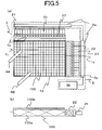
- Fig. 5(a) and Fig 5(b) show a position detecting device in Embodiment 2 of the present invention
- Fig. 5(a) is a top plan diagram outlining a configuration of the position detecting device
- Fig. 5(b) is a cross-sectional side diagram thereof (viewed from the bottom).
- a light-guide plate 100 is constructed of a first light-guide plate 100a made of a glass plate, and a second light-guide plate 100b that is softer and easier to be transformed than the first light-guide plate 100a and overlaid thereupon.
- Other constituent items are equivalent or similar to those in Embodiment 1.
- the same reference numerals and symbols designate the same items as or items corresponding to those described in Embodiment 1; thus their explanation is omitted.
- the first light-guide plate 100a is a square-shaped glass plate having a refractive index of some 1.5 and a thickness of some 5 mm; the second light-guide plate 100b is made of a soft resin having a refractive index of some 1.3.
- the light-guide plate 100 is constructed of the first light-guide plate 100a and the second light-guide plate 100b that is overlaid thereupon.
- the emitting unit 2 performs, via the optical processing units 22, adjustment of thickness-wise angles of the outputted light from the light sources 21 each into the light-guide plate, similarly to the manner as set forth in Embodiment 1, so that the emitted light (light beams each) is totally reflected at both inner surfaces of the light-guide plate 100.
- emitted light is totally reflected thickness-wise inside surfaces of the light-guide plate 100 by the part where the second light-guide plate 100b is closely contacted with the first light-guide plate 100a; by the part where the second light-guide plate 100b is not closely contacted with the first light-guide plate 100a, emitted light is totally reflected thickness-wise within the second light-guide plate 100b and also within the first light-guide plate 100a; thereby, without the light escaping at any parts of both surfaces of the light-guide plate 100, the emitted light (light beams each) is able to travel toward the opposing (other) side.
- an area of the light-guiding part 41 closely contacting the second light-guide plate 100b is increased; thus, it is possible to efficiently guide part of light traveling in the light-guide plate 100 into the light-guiding part 41. For this reason, it becomes easy to accurately detect a position of the indicating device 4.
- the light-guide plate 100 is constructed of the first light-guide plate 100a and the second light-guide plate 100b that is softer than the first light-guide plate 100a and overlaid thereupon, by easily detecting light traveling in the light-guide plate 100 without depending on the hardness and shape of the light-guiding part 41 of the indicating device 4, it becomes possible to detect a position of the indicating device 4 based on a detection signal and a scanned position of the emission-control unit 3.
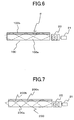
- Fig. 7 is a cross-sectional side view outlining a light-guide plate 200 of a position detecting device in Embodiment 3 of the present invention.
- the light-guide plate 200 is constructed of three layers of light-guide plates.
- Other constituent items are equivalent or similar to those in Embodiment 2.
- the same reference numerals and symbols designate the same items as or items corresponding to those described in Embodiment 2; thus their explanation is omitted.
- a first light-guide plate 200a is a square-shaped glass plate having the same refractive index of some 1.5 and thickness of some 5 mm as those in Embodiment 2.
- a third light-guide plate 200b is formed; what is more, upon the top surface of the third light-guide plate 200b, a fourth light-guide plate 200c is formed.
- a transparent material of high flexibility is used for the third light-guide plate 200b, it is possible to use, instead of solid material, a material of fluidity such as pure water and alcohol by tightly sealing it between the first light-guide plate 200a and the fourth light-guide plate 200c.
- a resin such as a thin acrylic film can be used.
- the optical processing units 22 each are adjusted so that angles of the light beams each reflecting thickness-wise within the light-guide plate 200 are set in such a manner that emitted light passes through boundaries between neighboring two of the light-guide plates 200a, 200b, and 200c, meanwhile, it is totally reflected by that between the light-guide plate 200 and the air.
- part of the top side of the light-guide plate 200 i.e., the fourth light-guide plate 200c
- the light-guiding part 41 is pressed by the light-guiding part 41 and is transformed or distorted similarly to the manner as set forth in Embodiment 2, so that angularities of the top side of the light-guide plate 200 change.
- an area of the light-guiding part 41 closely contacting the fourth light-guide plate 200c is increased; thus, it is possible to efficiently guide part of light traveling in the light-guide plate 200 into the light-guiding part 41.
- the light-guiding part 41 closely contacting the fourth light-guide plate 200c is overlaid upon the third light-guide plate 200b that is flexible or pliable, even when material of high strength is used for the fourth light-guide plate 200c, it can be transformed by reducing its thickness; therefore, it becomes possible to reduce friction between the light-guide plate 200 and the light-guiding part 41, and to reinforce the durability therewith against wear.
- the light-guide plate 200 is constructed of three layers of light-guide plates in which the third light-guide plate 200b of soft material is provided between the first light-guide plate 200a and the fourth light-guide plate 200c, it becomes possible to easily detect light traveling in the light-guide plate 200 without depending on the hardness and shape of the light-guiding part 41 of the indicating device 4; in addition, it becomes easy to reinforce the strength and durability of the top surface of the light-guide plate 200.
- the coordinate calculating unit 43 is provided in the indicating device 4, it may be possible to arrange that the indicating device 4 includes only those functions to detect light and to transmit a detection signal alone or together with an identification signal, and then, the coordinate outputting device 5 has the function to calculate a position of the indicating device 4.
- the light sources 21 each are provided according to the light beams each, and emission of the light beams is controlled by controlling powering on/off each of the light sources 21, it is possible to control the emission of the light beams each, while keeping the light sources 21 powered on, using shutters such as a liquid crystal display (LCD) provided at the outlets of the optical processing units 22, and the shutters are controlled open/close corresponding to the light beams each.
- shutters such as a liquid crystal display (LCD) provided at the outlets of the optical processing units 22, and the shutters are controlled open/close corresponding to the light beams each.
- one laser can be used as light sources for a plurality of light beams; therefore, the number of lasers can be reduced.
- a light-emitting diode may be used for the light sources 21.
- the light-emitting diode is inferior to the laser in a light-condensing characteristic, in order to maintain a position detecting accuracy, adjustment of the optical processing units 22 and the like is necessary according to the light sources 21 used.
- a resin such as acryl may be used.
Landscapes
- Engineering & Computer Science (AREA)
- General Engineering & Computer Science (AREA)
- Theoretical Computer Science (AREA)
- Human Computer Interaction (AREA)
- Physics & Mathematics (AREA)
- General Physics & Mathematics (AREA)
- Length Measuring Devices By Optical Means (AREA)
- Position Input By Displaying (AREA)
Applications Claiming Priority (1)
| Application Number | Priority Date | Filing Date | Title |
|---|---|---|---|
| JP2006344026A JP4775247B2 (ja) | 2006-12-21 | 2006-12-21 | 位置検出装置 |
Publications (3)
| Publication Number | Publication Date |
|---|---|
| EP1936478A2 true EP1936478A2 (fr) | 2008-06-25 |
| EP1936478A3 EP1936478A3 (fr) | 2009-01-07 |
| EP1936478B1 EP1936478B1 (fr) | 2009-12-30 |
Family
ID=38477315
Family Applications (1)
| Application Number | Title | Priority Date | Filing Date |
|---|---|---|---|
| EP07011905A Ceased EP1936478B1 (fr) | 2006-12-21 | 2007-06-18 | Dispositif de détection de position |
Country Status (6)
| Country | Link |
|---|---|
| US (1) | US8094138B2 (fr) |
| EP (1) | EP1936478B1 (fr) |
| JP (1) | JP4775247B2 (fr) |
| KR (1) | KR100907962B1 (fr) |
| CN (1) | CN101206550B (fr) |
| DE (1) | DE602007004058D1 (fr) |
Cited By (4)
| Publication number | Priority date | Publication date | Assignee | Title |
|---|---|---|---|---|
| WO2011031215A1 (fr) * | 2009-09-11 | 2011-03-17 | Flatfrog Laboratories Ab | Surface à effleurement à indice de réfraction variable |
| ITTN20090012A1 (it) * | 2009-09-25 | 2011-03-25 | Daniele Bernardini | Griglia optoelettronica per monitor industriali e commerciali con funzionalita' "multitouch screen" |
| EP2264566A3 (fr) * | 2009-06-13 | 2014-07-02 | Samsung Electronics Co., Ltd. | Dispositif de pointage, appareil d'affichage et système de pointage, et procédé de génération de données de localisation et procédé d'affichage l'utilisant |
| EP2390763A3 (fr) * | 2010-05-24 | 2014-07-23 | Samsung Electronics Co., Ltd. | Dispositif de pointage et appareil d'affichage |
Families Citing this family (57)
| Publication number | Priority date | Publication date | Assignee | Title |
|---|---|---|---|---|
| US20100085333A1 (en) * | 2007-01-30 | 2010-04-08 | Takayuki Akimoto | Input system and method, and computer program |
| JP5162706B2 (ja) | 2008-09-26 | 2013-03-13 | ヒューレット−パッカード デベロップメント カンパニー エル.ピー. | 撹乱光を使用したタッチロケーションの決定 |
| US20100079409A1 (en) * | 2008-09-29 | 2010-04-01 | Smart Technologies Ulc | Touch panel for an interactive input system, and interactive input system incorporating the touch panel |
| US8132948B2 (en) * | 2008-10-17 | 2012-03-13 | Microsoft Corporation | Method and apparatus for directing light around an obstacle using an optical waveguide for uniform lighting of a cylindrical cavity |
| SE533704C2 (sv) | 2008-12-05 | 2010-12-07 | Flatfrog Lab Ab | Pekkänslig apparat och förfarande för drivning av densamma |
| JP4683135B2 (ja) * | 2009-03-04 | 2011-05-11 | エプソンイメージングデバイス株式会社 | 位置検出機能付き表示装置および電子機器 |
| US8358901B2 (en) * | 2009-05-28 | 2013-01-22 | Microsoft Corporation | Optic having a cladding |
| KR101604030B1 (ko) | 2009-06-16 | 2016-03-16 | 삼성전자주식회사 | 어레이 방식의 후방 카메라를 이용한 멀티터치 센싱 장치 |
| CN101989148A (zh) * | 2009-08-04 | 2011-03-23 | 北京汇冠新技术股份有限公司 | 一种触摸屏 |
| US8730212B2 (en) * | 2009-08-21 | 2014-05-20 | Microsoft Corporation | Illuminator for touch- and object-sensitive display |
| JP5493702B2 (ja) | 2009-10-26 | 2014-05-14 | セイコーエプソン株式会社 | 位置検出機能付き投射型表示装置 |
| JP2011090604A (ja) * | 2009-10-26 | 2011-05-06 | Seiko Epson Corp | 光学式位置検出装置および位置検出機能付き表示装置 |
| JP5326989B2 (ja) | 2009-10-26 | 2013-10-30 | セイコーエプソン株式会社 | 光学式位置検出装置および位置検出機能付き表示装置 |
| JP2011099994A (ja) | 2009-11-06 | 2011-05-19 | Seiko Epson Corp | 位置検出機能付き投射型表示装置 |
| KR101588001B1 (ko) | 2009-11-16 | 2016-01-26 | 삼성디스플레이 주식회사 | 표시장치 |
| EP2333644B1 (fr) * | 2009-11-16 | 2014-12-10 | Samsung Display Co., Ltd. | Appareil d'affichage éco-énergétique avec capacité de détection d'objets |
| JP5549203B2 (ja) * | 2009-12-01 | 2014-07-16 | セイコーエプソン株式会社 | 光学式位置検出装置、ハンド装置およびタッチパネル |
| WO2011079670A1 (fr) * | 2009-12-28 | 2011-07-07 | 北京汇冠新技术股份有限公司 | Écran tactile et système tactile |
| KR101704695B1 (ko) * | 2010-03-09 | 2017-02-09 | 삼성디스플레이 주식회사 | 터치 위치 검출 방법, 이를 수행하기 위한 터치 위치 검출 장치 및 터치 위치 검출 장치를 포함하는 표시 장치 |
| TW201203052A (en) * | 2010-05-03 | 2012-01-16 | Flatfrog Lab Ab | Touch determination by tomographic reconstruction |
| TW201140202A (en) * | 2010-05-04 | 2011-11-16 | Chunghwa Picture Tubes Ltd | Photo-sensing touch LCD |
| CN102467302B (zh) * | 2010-11-05 | 2015-05-13 | 上海天马微电子有限公司 | 一种用于电容式触摸屏区分导电液体与手指的检测方法 |
| CN102023762B (zh) * | 2010-12-08 | 2013-02-06 | 成都际洲科技有限公司 | 一种光学多点触摸屏及其实现方法 |
| KR20130006165A (ko) * | 2011-07-08 | 2013-01-16 | 삼성전자주식회사 | 터치 인식 방법 및 이를 적용한 디스플레이 시스템 |
| CN102880351B (zh) * | 2011-07-11 | 2015-06-03 | 友碁科技股份有限公司 | 用于光学式触控面板的触碰点定位方法及用于光学式触控面板的触碰点定位装置 |
| US10168835B2 (en) | 2012-05-23 | 2019-01-01 | Flatfrog Laboratories Ab | Spatial resolution in touch displays |
| US10019113B2 (en) | 2013-04-11 | 2018-07-10 | Flatfrog Laboratories Ab | Tomographic processing for touch detection |
| US9874978B2 (en) | 2013-07-12 | 2018-01-23 | Flatfrog Laboratories Ab | Partial detect mode |
| CN104423736A (zh) * | 2013-08-29 | 2015-03-18 | 天津富纳源创科技有限公司 | 触摸屏触摸识别方法 |
| US10146376B2 (en) | 2014-01-16 | 2018-12-04 | Flatfrog Laboratories Ab | Light coupling in TIR-based optical touch systems |
| US10126882B2 (en) | 2014-01-16 | 2018-11-13 | Flatfrog Laboratories Ab | TIR-based optical touch systems of projection-type |
| WO2015199602A1 (fr) | 2014-06-27 | 2015-12-30 | Flatfrog Laboratories Ab | Détection de contamination de surface |
| US10423281B2 (en) | 2014-08-27 | 2019-09-24 | Hewlett-Packard Development Company, L.P. | Screen contact detection using total internal reflection |
| CN105573570B (zh) * | 2014-11-07 | 2018-06-19 | 上海科勒电子科技有限公司 | 一种电容触控屏的触摸按键识别方法 |
| CN105630256B (zh) * | 2014-11-07 | 2018-07-17 | 上海科勒电子科技有限公司 | 一种电容触控屏的触摸按键识别方法 |
| CN104484064B (zh) | 2014-12-30 | 2018-04-27 | 合肥鑫晟光电科技有限公司 | 用于触摸显示屏的主动笔、触摸显示屏及触控输入系统 |
| EP3250993B1 (fr) | 2015-01-28 | 2019-09-04 | FlatFrog Laboratories AB | Trames de quarantaine tactiles dynamiques |
| US10318074B2 (en) | 2015-01-30 | 2019-06-11 | Flatfrog Laboratories Ab | Touch-sensing OLED display with tilted emitters |
| EP3537269A1 (fr) | 2015-02-09 | 2019-09-11 | FlatFrog Laboratories AB | Système tactile optique |
| CN107250855A (zh) | 2015-03-02 | 2017-10-13 | 平蛙实验室股份公司 | 用于光耦合的光学部件 |
| EP3387516B1 (fr) | 2015-12-09 | 2022-04-20 | FlatFrog Laboratories AB | Identification de stylet améliorée |
| WO2017203355A1 (fr) * | 2016-05-23 | 2017-11-30 | Rapt Ip Limited | Détection d'instruments à l'aide d'un dispositif tactile optique, avec association de contacts avec des instruments actifs |
| CN108062175B (zh) * | 2016-11-07 | 2021-11-23 | 中兴通讯股份有限公司 | 屏幕操作控制方法、装置及终端 |
| WO2018096430A1 (fr) | 2016-11-24 | 2018-05-31 | Flatfrog Laboratories Ab | Optimisation automatique de signal tactile |
| KR102629629B1 (ko) | 2016-12-07 | 2024-01-29 | 플라트프로그 라보라토리즈 에이비 | 개선된 터치 장치 |
| CN110300950B (zh) | 2017-02-06 | 2023-06-16 | 平蛙实验室股份公司 | 触摸感测系统中的光学耦合 |
| WO2018174786A1 (fr) | 2017-03-22 | 2018-09-27 | Flatfrog Laboratories | Différenciation de stylo pour écrans tactiles |
| WO2018182476A1 (fr) | 2017-03-28 | 2018-10-04 | Flatfrog Laboratories Ab | Appareil de détection tactile et son procédé d'assemblage |
| CN111052058B (zh) | 2017-09-01 | 2023-10-20 | 平蛙实验室股份公司 | 改进的光学部件 |
| US11567610B2 (en) | 2018-03-05 | 2023-01-31 | Flatfrog Laboratories Ab | Detection line broadening |
| CN112889016A (zh) | 2018-10-20 | 2021-06-01 | 平蛙实验室股份公司 | 用于触摸敏感装置的框架及其工具 |
| CN109558031B (zh) * | 2018-11-28 | 2021-09-28 | 合肥工业大学 | 一种红外触摸屏上触点检测方法 |
| WO2020153890A1 (fr) | 2019-01-25 | 2020-07-30 | Flatfrog Laboratories Ab | Terminal de visioconférence son procédé de fonctionnement |
| EP4066089B1 (fr) | 2019-11-25 | 2024-09-25 | FlatFrog Laboratories AB | Un appareil de détection tactile |
| WO2021158164A1 (fr) | 2020-02-08 | 2021-08-12 | Flatfrog Laboratories Ab | Appareil tactile à interactions à faible latence |
| CN115039063B (zh) | 2020-02-10 | 2026-02-13 | 平蛙实验室股份公司 | 改进的触摸感测设备 |
| US12353649B2 (en) * | 2022-06-29 | 2025-07-08 | Apple Inc. | Input device with optical sensors |
Citations (4)
| Publication number | Priority date | Publication date | Assignee | Title |
|---|---|---|---|---|
| JP2000172444A (ja) | 1998-10-02 | 2000-06-23 | Semiconductor Energy Lab Co Ltd | タッチパネル及びタッチパネルを備えた表示装置及び表示装置を備えた電子機器 |
| EP1408396A2 (fr) | 2002-10-04 | 2004-04-14 | SMK Corporation | Dispositif d'entrée avec pointage |
| US6972753B1 (en) | 1998-10-02 | 2005-12-06 | Semiconductor Energy Laboratory Co., Ltd. | Touch panel, display device provided with touch panel and electronic equipment provided with display device |
| JP2005339342A (ja) | 2004-05-28 | 2005-12-08 | Noritz Corp | 光学式タッチパネル装置 |
Family Cites Families (15)
| Publication number | Priority date | Publication date | Assignee | Title |
|---|---|---|---|---|
| JPS52129327A (en) * | 1976-04-23 | 1977-10-29 | Nec Corp | Input tablet |
| JPH02123626A (ja) * | 1988-11-01 | 1990-05-11 | Mitsubishi Electric Corp | 光スイツチ装置 |
| JPH0540574A (ja) * | 1991-08-06 | 1993-02-19 | Fujitsu Ltd | 位置認識装置 |
| JP3277645B2 (ja) * | 1993-11-01 | 2002-04-22 | 株式会社日立製作所 | ペン入力式情報処理装置 |
| TW523627B (en) * | 1998-07-14 | 2003-03-11 | Hitachi Ltd | Liquid crystal display device |
| US6597348B1 (en) * | 1998-12-28 | 2003-07-22 | Semiconductor Energy Laboratory Co., Ltd. | Information-processing device |
| US6559827B1 (en) * | 2000-08-16 | 2003-05-06 | Gateway, Inc. | Display assembly |
| JP4538933B2 (ja) * | 2000-10-06 | 2010-09-08 | 三菱電機株式会社 | 位置検出機能つき液晶表示装置 |
| KR100568583B1 (ko) * | 2002-10-23 | 2006-04-07 | 주식회사 애트랩 | 광 커서 제어장치 |
| US20060279558A1 (en) * | 2003-09-22 | 2006-12-14 | Koninklike Phillips Electronics N.V. | Touc input screen using a light guide |
| JP2005107890A (ja) * | 2003-09-30 | 2005-04-21 | Sanyo Electric Co Ltd | El表示装置 |
| US7298367B2 (en) * | 2003-11-25 | 2007-11-20 | 3M Innovative Properties Company | Light emitting stylus and user input device using same |
| US7385594B2 (en) * | 2004-02-19 | 2008-06-10 | Au Optronics Corporation | Position encoded sensing device and a method thereof |
| US20060001654A1 (en) * | 2004-06-30 | 2006-01-05 | National Semiconductor Corporation | Apparatus and method for performing data entry with light based touch screen displays |
| US8130210B2 (en) * | 2004-11-30 | 2012-03-06 | Avago Technologies Ecbu Ip (Singapore) Pte. Ltd. | Touch input system using light guides |
-
2006
- 2006-12-21 JP JP2006344026A patent/JP4775247B2/ja not_active Expired - Fee Related
-
2007
- 2007-06-18 EP EP07011905A patent/EP1936478B1/fr not_active Ceased
- 2007-06-18 DE DE602007004058T patent/DE602007004058D1/de active Active
- 2007-07-19 CN CN2007101361651A patent/CN101206550B/zh not_active Expired - Fee Related
- 2007-08-08 US US11/889,041 patent/US8094138B2/en not_active Expired - Fee Related
- 2007-08-30 KR KR1020070087626A patent/KR100907962B1/ko not_active Expired - Fee Related
Patent Citations (4)
| Publication number | Priority date | Publication date | Assignee | Title |
|---|---|---|---|---|
| JP2000172444A (ja) | 1998-10-02 | 2000-06-23 | Semiconductor Energy Lab Co Ltd | タッチパネル及びタッチパネルを備えた表示装置及び表示装置を備えた電子機器 |
| US6972753B1 (en) | 1998-10-02 | 2005-12-06 | Semiconductor Energy Laboratory Co., Ltd. | Touch panel, display device provided with touch panel and electronic equipment provided with display device |
| EP1408396A2 (fr) | 2002-10-04 | 2004-04-14 | SMK Corporation | Dispositif d'entrée avec pointage |
| JP2005339342A (ja) | 2004-05-28 | 2005-12-08 | Noritz Corp | 光学式タッチパネル装置 |
Cited By (5)
| Publication number | Priority date | Publication date | Assignee | Title |
|---|---|---|---|---|
| EP2264566A3 (fr) * | 2009-06-13 | 2014-07-02 | Samsung Electronics Co., Ltd. | Dispositif de pointage, appareil d'affichage et système de pointage, et procédé de génération de données de localisation et procédé d'affichage l'utilisant |
| WO2011031215A1 (fr) * | 2009-09-11 | 2011-03-17 | Flatfrog Laboratories Ab | Surface à effleurement à indice de réfraction variable |
| US9035909B2 (en) | 2009-09-11 | 2015-05-19 | Flatfrog Laboratories Ab | Touch surface with variable refractive index |
| ITTN20090012A1 (it) * | 2009-09-25 | 2011-03-25 | Daniele Bernardini | Griglia optoelettronica per monitor industriali e commerciali con funzionalita' "multitouch screen" |
| EP2390763A3 (fr) * | 2010-05-24 | 2014-07-23 | Samsung Electronics Co., Ltd. | Dispositif de pointage et appareil d'affichage |
Also Published As
| Publication number | Publication date |
|---|---|
| EP1936478B1 (fr) | 2009-12-30 |
| CN101206550B (zh) | 2012-06-20 |
| DE602007004058D1 (de) | 2010-02-11 |
| US20080150915A1 (en) | 2008-06-26 |
| JP2008158616A (ja) | 2008-07-10 |
| EP1936478A3 (fr) | 2009-01-07 |
| JP4775247B2 (ja) | 2011-09-21 |
| KR20080058150A (ko) | 2008-06-25 |
| US8094138B2 (en) | 2012-01-10 |
| KR100907962B1 (ko) | 2009-07-16 |
| CN101206550A (zh) | 2008-06-25 |
Similar Documents
| Publication | Publication Date | Title |
|---|---|---|
| US8094138B2 (en) | Position detecting device | |
| EP2550584B1 (fr) | Agencement de lentilles pour un écran tactile basé sur la lumière | |
| US8896575B2 (en) | Pressure-sensitive touch screen | |
| US9389730B2 (en) | Light-based touch screen using elongated light guides | |
| US8587562B2 (en) | Light-based touch screen using elliptical and parabolic reflectors | |
| US9195344B2 (en) | Optical surface using a reflected image for determining three-dimensional position information | |
| US9436318B2 (en) | Coordinate detecting apparatus, method of detecting coordinate, and electronic information board system | |
| US8902435B2 (en) | Position detection apparatus and image display apparatus | |
| US20110163998A1 (en) | Light-based touch screen with shift-aligned emitter and receiver lenses | |
| US20110169781A1 (en) | Touch screen calibration and update methods | |
| US8403203B2 (en) | Component bonding using a capillary effect | |
| US9678663B2 (en) | Display system and operation input method | |
| KR20120058594A (ko) | 향상된 신호 대 노이즈비(snr)를 갖는 인터랙티브 입력 시스템 및 이미지 캡처 방법 | |
| CN101582001A (zh) | 触控屏幕、触控模块及控制方法 | |
| US9501160B2 (en) | Coordinate detection system and information processing apparatus | |
| CN101802759A (zh) | 低剖面触摸面板系统 | |
| JP2019053749A (ja) | ディスプレイ及びこれを用いた非接触入力装置 | |
| US20110096030A1 (en) | Optical position detecting device and display device with position detecting function | |
| US20150015545A1 (en) | Pointing input system having sheet-like light beam layer | |
| JP5335923B2 (ja) | 位置認識センサ、電子機器、及び表示装置 | |
| JP5944255B2 (ja) | 発光部を有する操作部材、およびそれを備えた座標入力システム | |
| CN102129330A (zh) | 触控屏幕、触控模块及控制方法 | |
| AU2014233573B2 (en) | Lens arrangement for light-based touch screen | |
| KR200244380Y1 (ko) | 태블릿 장치 | |
| JP2013232095A (ja) | 座標入力装置及び座標入力システム |
Legal Events
| Date | Code | Title | Description |
|---|---|---|---|
| PUAI | Public reference made under article 153(3) epc to a published international application that has entered the european phase |
Free format text: ORIGINAL CODE: 0009012 |
|
| AK | Designated contracting states |
Kind code of ref document: A2 Designated state(s): AT BE BG CH CY CZ DE DK EE ES FI FR GB GR HU IE IS IT LI LT LU LV MC MT NL PL PT RO SE SI SK TR |
|
| AX | Request for extension of the european patent |
Extension state: AL BA HR MK RS |
|
| PUAL | Search report despatched |
Free format text: ORIGINAL CODE: 0009013 |
|
| AK | Designated contracting states |
Kind code of ref document: A3 Designated state(s): AT BE BG CH CY CZ DE DK EE ES FI FR GB GR HU IE IS IT LI LT LU LV MC MT NL PL PT RO SE SI SK TR |
|
| AX | Request for extension of the european patent |
Extension state: AL BA HR MK RS |
|
| 17P | Request for examination filed |
Effective date: 20090115 |
|
| 17Q | First examination report despatched |
Effective date: 20090223 |
|
| GRAP | Despatch of communication of intention to grant a patent |
Free format text: ORIGINAL CODE: EPIDOSNIGR1 |
|
| GRAS | Grant fee paid |
Free format text: ORIGINAL CODE: EPIDOSNIGR3 |
|
| AKX | Designation fees paid |
Designated state(s): DE FR GB IT |
|
| GRAA | (expected) grant |
Free format text: ORIGINAL CODE: 0009210 |
|
| AK | Designated contracting states |
Kind code of ref document: B1 Designated state(s): DE FR GB IT |
|
| REG | Reference to a national code |
Ref country code: GB Ref legal event code: FG4D |
|
| REF | Corresponds to: |
Ref document number: 602007004058 Country of ref document: DE Date of ref document: 20100211 Kind code of ref document: P |
|
| PLBE | No opposition filed within time limit |
Free format text: ORIGINAL CODE: 0009261 |
|
| STAA | Information on the status of an ep patent application or granted ep patent |
Free format text: STATUS: NO OPPOSITION FILED WITHIN TIME LIMIT |
|
| 26N | No opposition filed |
Effective date: 20101001 |
|
| PG25 | Lapsed in a contracting state [announced via postgrant information from national office to epo] |
Ref country code: IT Free format text: LAPSE BECAUSE OF NON-PAYMENT OF DUE FEES Effective date: 20100618 |
|
| REG | Reference to a national code |
Ref country code: FR Ref legal event code: PLFP Year of fee payment: 10 |
|
| REG | Reference to a national code |
Ref country code: FR Ref legal event code: PLFP Year of fee payment: 11 |
|
| PGFP | Annual fee paid to national office [announced via postgrant information from national office to epo] |
Ref country code: FR Payment date: 20170511 Year of fee payment: 11 Ref country code: DE Payment date: 20170613 Year of fee payment: 11 Ref country code: GB Payment date: 20170614 Year of fee payment: 11 |
|
| PGFP | Annual fee paid to national office [announced via postgrant information from national office to epo] |
Ref country code: IT Payment date: 20170619 Year of fee payment: 11 |
|
| REG | Reference to a national code |
Ref country code: DE Ref legal event code: R119 Ref document number: 602007004058 Country of ref document: DE |
|
| GBPC | Gb: european patent ceased through non-payment of renewal fee |
Effective date: 20180618 |
|
| PG25 | Lapsed in a contracting state [announced via postgrant information from national office to epo] |
Ref country code: IT Free format text: LAPSE BECAUSE OF NON-PAYMENT OF DUE FEES Effective date: 20180618 Ref country code: FR Free format text: LAPSE BECAUSE OF NON-PAYMENT OF DUE FEES Effective date: 20180630 Ref country code: DE Free format text: LAPSE BECAUSE OF NON-PAYMENT OF DUE FEES Effective date: 20190101 Ref country code: GB Free format text: LAPSE BECAUSE OF NON-PAYMENT OF DUE FEES Effective date: 20180618 |