EP1936791A2 - Convertisseur à découpage - Google Patents
Convertisseur à découpage Download PDFInfo
- Publication number
- EP1936791A2 EP1936791A2 EP07116886A EP07116886A EP1936791A2 EP 1936791 A2 EP1936791 A2 EP 1936791A2 EP 07116886 A EP07116886 A EP 07116886A EP 07116886 A EP07116886 A EP 07116886A EP 1936791 A2 EP1936791 A2 EP 1936791A2
- Authority
- EP
- European Patent Office
- Prior art keywords
- voltage
- limiting
- capacitors
- diode
- switching
- Prior art date
- Legal status (The legal status is an assumption and is not a legal conclusion. Google has not performed a legal analysis and makes no representation as to the accuracy of the status listed.)
- Withdrawn
Links
Images
Classifications
-
- H—ELECTRICITY
- H02—GENERATION; CONVERSION OR DISTRIBUTION OF ELECTRIC POWER
- H02M—APPARATUS FOR CONVERSION BETWEEN AC AND AC, BETWEEN AC AND DC, OR BETWEEN DC AND DC, AND FOR USE WITH MAINS OR SIMILAR POWER SUPPLY SYSTEMS; CONVERSION OF DC OR AC INPUT POWER INTO SURGE OUTPUT POWER; CONTROL OR REGULATION THEREOF
- H02M3/00—Conversion of DC power input into DC power output
- H02M3/22—Conversion of DC power input into DC power output with intermediate conversion into AC
- H02M3/24—Conversion of DC power input into DC power output with intermediate conversion into AC by static converters
- H02M3/28—Conversion of DC power input into DC power output with intermediate conversion into AC by static converters using discharge tubes with control electrode or semiconductor devices with control electrode to produce the intermediate AC
- H02M3/325—Conversion of DC power input into DC power output with intermediate conversion into AC by static converters using discharge tubes with control electrode or semiconductor devices with control electrode to produce the intermediate AC using devices of a triode or a transistor type requiring continuous application of a control signal
- H02M3/335—Conversion of DC power input into DC power output with intermediate conversion into AC by static converters using discharge tubes with control electrode or semiconductor devices with control electrode to produce the intermediate AC using devices of a triode or a transistor type requiring continuous application of a control signal using semiconductor devices only
- H02M3/3353—Conversion of DC power input into DC power output with intermediate conversion into AC by static converters using discharge tubes with control electrode or semiconductor devices with control electrode to produce the intermediate AC using devices of a triode or a transistor type requiring continuous application of a control signal using semiconductor devices only having at least two simultaneously operating switches on the input side, e.g. "double forward" or "double (switched) flyback" converter
-
- H—ELECTRICITY
- H02—GENERATION; CONVERSION OR DISTRIBUTION OF ELECTRIC POWER
- H02M—APPARATUS FOR CONVERSION BETWEEN AC AND AC, BETWEEN AC AND DC, OR BETWEEN DC AND DC, AND FOR USE WITH MAINS OR SIMILAR POWER SUPPLY SYSTEMS; CONVERSION OF DC OR AC INPUT POWER INTO SURGE OUTPUT POWER; CONTROL OR REGULATION THEREOF
- H02M1/00—Details of apparatus for conversion
- H02M1/32—Means for protecting converters other than automatic disconnection
- H02M1/34—Snubber circuits
- H02M1/348—Passive dissipative snubbers
Definitions
- the invention relates to a switching converter having a primary-side transformer winding, the first winding terminal is connected via a first switching element to a supply voltage and the second winding terminal is connected via a second switching element to a reference potential.
- the primary-side clocks takes place by means of electronic switching elements. These switching elements must be designed so that on the one hand only small losses occur on the one hand and on the other hand, they permanently withstand the applied voltages. In this case, switching elements such as e.g. Switching transistors for low voltages cheaper than those that are suitable for switching higher voltages. In addition, particularly voltage-resistant switching transistors have poor electrical properties.
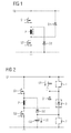
- FIG. 1 an exemplary circuit arrangement according to the prior art is shown.
- the two switching elements are always switched simultaneously.
- excess energy remains in the transformer. Before the next clock cycle can begin, this energy must be released. This is achieved by the arrangement of Abmagnetleiterstechnischen in which Abmagnetmaschinesdioden are arranged, via which current after switching off the switching elements current flows back into the supply circuit.
- the polarity of the voltage is reversed at the transformer and the voltage becomes so high until a current flow is established.
- the voltage load on a switching element then corresponds to the supply voltage plus the diode voltage of a demagnetization diode.
- the invention is therefore based on the object to provide an improvement over the prior art for a switching converter of the type mentioned.
- this object is achieved by a switching converter having a primary-side transformer winding whose first winding connection is connected to a supply voltage via a first switching element and whose second winding connection is connected to a reference potential via a second switching element, wherein the second winding connection via a first diode and a first Capacitor is connected to the supply voltage and wherein the first winding terminal is connected via a second diode and a second capacitor to the reference potential and further wherein a device for generating a bias voltage is connected to each capacitor.
- the polarity of the capacitors is chosen so that the Abmagnet Deutschensstrom from the positive pole of the second capacitor via the transformer winding to the negative pole of the first capacitor fliest.
- the voltage peaks occurring at the time of switching off the switching elements are lower by the amount of bias in the capacitors than in a direct connection of the Abmagnetleiters effeten to the supply circuit.
- the inventive arrangement thus enables the use of switching elements, which must have a correspondingly lower dielectric strength and thus have better electrical properties and also are cheaper.
- a first element for limiting the voltage and balancing the two capacitors and parallel to the second capacitor a second element for limiting the voltage and balancing the two capacitors is provided parallel to the first capacitor. Furthermore, the first and the second element for limiting the voltage and balancing the two capacitors via a further voltage-limiting Element interconnected.
- the corresponding elements are connected in the manner between supply voltage and reference potential, that symmetrical bias voltages with the intended polarities are applied to the two capacitors, without the need for an additional voltage source is required.
- the voltage limiting and balancing elements of the two capacitors determine the bias on the capacitors. In order to keep the capacitors charged, the further voltage-limiting element is provided.
- the first element for limiting the voltage and balancing the two capacitors comprises a series connection of a first resistor and a third voltage-limiting diode with a second resistor arranged in parallel to this series circuit and if the second element for limiting the voltage and balancing the two capacitors, a series circuit a third resistor and a fourth voltage-limiting diode having a fourth resistor arranged parallel to said series circuit, and in addition, if the further voltage-limiting element comprises a fifth voltage-limiting diode with a fifth resistor arranged in series.
- the desired bias is reliably applied to the capacitors.
- resistors and voltage limiting diodes the bias on the capacitors can be kept within narrow limits.
- Another advantageous embodiment provides that the first element for limiting the voltage and balancing the two capacitors from a third voltage-limiting diode is formed and that the second element for limiting the voltage and balancing the two capacitors from a fourth voltage-limiting diode is formed and that the further voltage-limiting Element is designed as a fifth voltage-limiting diode. If fluctuations in the supply voltage are precluded or at least negligible in relation to the voltage fluctuations on the capacitors, the biasing of the capacitors can be achieved with voltage-limiting diodes alone. It is advantageous for all embodiments, if the voltage-limiting diodes are designed as Zener diodes or as suppressor diodes. Zener diodes have the advantage that they are cheap and easy to obtain. At suppressor diodes, the voltage increases even less at very high currents than at Zener diodes. They have a higher discharge capacity than zener diodes.
- the first element for limiting the voltage and balancing the two capacitors from a first resistor and the second element for limiting the voltage and balancing the two capacitors are formed from a third resistor.
- the further voltage-limiting element is designed as a fifth resistor. The circuit thus builds up in a simple manner only from resistors.
- the invention is also advantageously applicable to a circuit arrangement which, in addition to a switching converter, provides an additional stable auxiliary voltage source, e.g. for supplying control elements.
- the auxiliary voltage source then supplies the bias to the capacitors by the capacitors are connected directly or by means of various voltage-limiting elements to the auxiliary voltage source.
- switching elements are designed as switching transistors.
- Switching transistors are on the one hand inexpensive and are on the other hand due to their electrical properties very well suited for use in switching converters.
- FIG. 1 a primary-side arrangement according to the prior art is shown.
- the primary winding P of a transformer is connected to a first connection via a first switching element S1 to a supply voltage Uz and to a second connection via a second switching element S2 to a reference potential.
- the second terminal of the primary winding P is further connected to the anode of a first diode D1, wherein the cathode of this first diode D1 is connected to the supply voltage.
- the first terminal is further connected to the cathode of a second diode D2, wherein the anode of this second diode D2 is in turn connected to the reference potential.
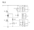
- FIG. 2 An exemplary embodiment of an arrangement according to the invention is shown in FIG. 2 shown.
- the arrangement builds on the in FIG. 1 shown, with the difference that the cathode of the first diode D1 is connected via a first capacitor C1 to the supply voltage Uz and that the anodes of the second diode D2 is connected via a second capacitor C2 to the reference potential.
- a first element for limiting the voltage and balancing the two capacitors 1 is also provided.
- a second element for limiting the voltage and balancing the two capacitors 2 is arranged parallel to the second capacitor C2. These elements cause the bias on the capacitors C1, C2.
- the cathode of the first diode D1 is connected via a voltage-limiting element 3 to the anode of the second diode D2. With this voltage-limiting element 3, the capacitors C1, C2 are kept charged.
- the two capacitors C1, C2 are biased in the manner U1, U2, that at the first capacitor C1, a first positive bias voltage U1 from the terminal to the supply voltage Uz to the cathode of the first diode D1 is applied and that the second capacitor C2 a second positive bias voltage U2 from the anode of the second diode D2 to the connection point is applied to the reference potential.
- the bias voltages U1, U2 on the capacitors C1, C2 are decisive for the voltage load of the switching elements S1, S2.
- the bias voltages U1, U2 at the capacitors C1, C2 is chosen so that the flux losses and turn-on delays of the diodes D1, D2 are compensated.
- the size of the capacitors C1, C2 is chosen so that a Abmagnettechnischsvorgang generates only a small voltage swing.
- the elements for limiting the voltage and balancing the two capacitors 1, 2 are replaced by an auxiliary voltage source.
- the further voltage-limiting element 3 is not required.
- FIG. 3 is an example of the design of the elements for limiting the voltage and balancing of the two capacitors 1, 2 (eg per 100nF / 200V) and the other voltage-limiting element 3 shown.
- a series circuit of a first resistor R1 eg 10k ⁇
- a suppressor diode third voltage-limiting diode D3 eg 130V breakdown voltage
- a second resistor R2 eg 200k ⁇
- the series circuit and the second resistor R2 form the first element for limiting the voltage and balancing the two capacitors 1.
- a series arrangement of a third resistor R3 (e.g., 10k ⁇ ) and a fourth voltage-limiting diode D4 (e.g., 130V breakdown voltage) formed as a suppressor diode is arranged in parallel with the second capacitor C2.
- a fourth resistor R4 (e.g., 200k ⁇ ) is connected in parallel with this series connection. This series connection and the fourth resistor R4 form the second element for limiting the voltage and balancing the two capacitors 2.
- the two elements for limiting the voltage and symmetrizing the two capacitors 1, 2 cause the bias voltages U1, U2 applied to the capacitors C1, C2 to be approximately equal.
- the further voltage-limiting element 3 is formed of a fifth resistor (eg, 1k ⁇ ) and a fifth voltage-limiting diode D5 (eg, 440V breakdown voltage) arranged in series therewith, designed as a suppressor diode.
- the two diodes D1, D2 in the Abmagnetleiters admiren are designed with a supply voltage of 800 V, for example, up to 800 V, as well as the two switching elements S1 and S2.
Landscapes
- Engineering & Computer Science (AREA)
- Power Engineering (AREA)
- Dc-Dc Converters (AREA)
Applications Claiming Priority (1)
| Application Number | Priority Date | Filing Date | Title |
|---|---|---|---|
| AT0208406A AT504122B1 (de) | 2006-12-19 | 2006-12-19 | Schaltwandler |
Publications (2)
| Publication Number | Publication Date |
|---|---|
| EP1936791A2 true EP1936791A2 (fr) | 2008-06-25 |
| EP1936791A3 EP1936791A3 (fr) | 2016-06-08 |
Family
ID=39154306
Family Applications (1)
| Application Number | Title | Priority Date | Filing Date |
|---|---|---|---|
| EP07116886.8A Withdrawn EP1936791A3 (fr) | 2006-12-19 | 2007-09-21 | Convertisseur à découpage |
Country Status (2)
| Country | Link |
|---|---|
| EP (1) | EP1936791A3 (fr) |
| AT (1) | AT504122B1 (fr) |
Cited By (1)
| Publication number | Priority date | Publication date | Assignee | Title |
|---|---|---|---|---|
| EP2187515A1 (fr) * | 2008-11-12 | 2010-05-19 | Magneti Marelli S.p.A. | Appareil convertisseur courant continu à découpage direct et procédé de conversion correspondant |
Family Cites Families (4)
| Publication number | Priority date | Publication date | Assignee | Title |
|---|---|---|---|---|
| US4403269A (en) * | 1982-03-05 | 1983-09-06 | International Business Machines Corporation | Non-dissipative snubber circuit apparatus |
| SU1101988A1 (ru) * | 1982-06-11 | 1984-07-07 | Научно-Исследовательский Институт Автоматики И Электромеханики При Томском Институте Автоматизированных Систем Управления И Радиоэлектроники | Преобразователь напр жени |
| JP3268118B2 (ja) * | 1994-05-16 | 2002-03-25 | ケイディーディーアイ株式会社 | 直流安定化電源装置 |
| US5883793A (en) * | 1998-04-30 | 1999-03-16 | Lucent Technologies Inc. | Clamp circuit for a power converter and method of operation thereof |
-
2006
- 2006-12-19 AT AT0208406A patent/AT504122B1/de not_active IP Right Cessation
-
2007
- 2007-09-21 EP EP07116886.8A patent/EP1936791A3/fr not_active Withdrawn
Cited By (1)
| Publication number | Priority date | Publication date | Assignee | Title |
|---|---|---|---|---|
| EP2187515A1 (fr) * | 2008-11-12 | 2010-05-19 | Magneti Marelli S.p.A. | Appareil convertisseur courant continu à découpage direct et procédé de conversion correspondant |
Also Published As
| Publication number | Publication date |
|---|---|
| AT504122A4 (de) | 2008-03-15 |
| AT504122B1 (de) | 2008-03-15 |
| EP1936791A3 (fr) | 2016-06-08 |
Similar Documents
| Publication | Publication Date | Title |
|---|---|---|
| DE102005002360B4 (de) | Tiefsetzer, Verfahren zur Ansteuerung und Verwendung des Tiefsetzers | |
| DE102007061978A1 (de) | Schaltungsanordnung zum Bereitstellen einer Spannungsversorgung für eine Transistor-Treiberschaltung | |
| DE3111757A1 (de) | Steuerschaltung fuer einen vollsteuergate-thyristor | |
| EP0123085A2 (fr) | Bloc d'alimentation à commutation électronique avec bobine de transformateur | |
| EP2208400B1 (fr) | Alimentation en courant commutable pour circuits auxiliaires dans un convertisseur | |
| DE102013109797A1 (de) | Ionisator | |
| DE102005030601A1 (de) | Netzteil mit Vollbrückenschaltung und großem Regelungsbereich | |
| DE19614816C1 (de) | Elektronisches Schaltnetzteil und dessen Verwendung | |
| EP1936791A2 (fr) | Convertisseur à découpage | |
| EP0266743B1 (fr) | Disposition de circuit pour produire une tension d'alimentation interne dans une alimentation de courant à découpage | |
| EP0259845A2 (fr) | Protection contre l'inversion de polarité et contre les tensions alternatives pour les consommateurs électriques à courant continu | |
| WO2001017098A1 (fr) | Alimentation a decoupage pourvue d'un dispositif limitant la tension de sortie | |
| DE4205099C1 (en) | Voltage inverter for use with battery supply - has DC=DC and DC=AC stages with sensor circuit control for generation of either 300 V DC or 220 V AC | |
| DE60212563T2 (de) | Leistungsschaltung einer Plasmadisplay | |
| EP1919067B1 (fr) | Circuit de contrôle pour un commutateur dans une alimentation à découpage avec mode rafale | |
| DE102010013537B4 (de) | Gleichspannungswandler mit Cuk-Schaltung | |
| DE3300285C2 (de) | Elektronisches Schaltnetzteil | |
| DE3311737C2 (de) | Elektronisches Schaltnetzteil | |
| EP2140735B1 (fr) | Ensemble circuit servant à amorcer et à faire fonctionner au moins une lampe à décharge | |
| DE102010002231A1 (de) | Verfahren und Schaltung zur Erzeugung eines Spannungspulses > 500V. | |
| DE3232237C2 (de) | Elektronisches Schaltnetzteil | |
| DE102019206636B4 (de) | Schaltnetzteil | |
| DE102013203014B4 (de) | Spannungsversorgungsvorrichtung mit einer Schaltungsanordnung zum schnellen Entladen zumindest eines Kondensators | |
| DE102024206164A1 (de) | 1Active-Clamp-Flyback-Konverter und Betriebsverfahren hierfür | |
| DE3726149C2 (fr) |
Legal Events
| Date | Code | Title | Description |
|---|---|---|---|
| PUAI | Public reference made under article 153(3) epc to a published international application that has entered the european phase |
Free format text: ORIGINAL CODE: 0009012 |
|
| AK | Designated contracting states |
Kind code of ref document: A2 Designated state(s): AT BE BG CH CY CZ DE DK EE ES FI FR GB GR HU IE IS IT LI LT LU LV MC MT NL PL PT RO SE SI SK TR |
|
| AX | Request for extension of the european patent |
Extension state: AL BA HR MK RS |
|
| RAP1 | Party data changed (applicant data changed or rights of an application transferred) |
Owner name: SIEMENS AKTIENGESELLSCHAFT |
|
| RAP1 | Party data changed (applicant data changed or rights of an application transferred) |
Owner name: SIEMENS AKTIENGESELLSCHAFT |
|
| PUAL | Search report despatched |
Free format text: ORIGINAL CODE: 0009013 |
|
| AK | Designated contracting states |
Kind code of ref document: A3 Designated state(s): AT BE BG CH CY CZ DE DK EE ES FI FR GB GR HU IE IS IT LI LT LU LV MC MT NL PL PT RO SE SI SK TR |
|
| AX | Request for extension of the european patent |
Extension state: AL BA HR MK RS |
|
| RIC1 | Information provided on ipc code assigned before grant |
Ipc: H02M 3/155 20060101AFI20160429BHEP Ipc: H02M 3/335 20060101ALI20160429BHEP Ipc: H02M 1/34 20070101ALI20160429BHEP |
|
| STAA | Information on the status of an ep patent application or granted ep patent |
Free format text: STATUS: THE APPLICATION HAS BEEN PUBLISHED |
|
| AKY | No designation fees paid | ||
| AXX | Extension fees paid |
Extension state: MK Extension state: RS Extension state: BA Extension state: HR Extension state: AL |
|
| REG | Reference to a national code |
Ref country code: DE Ref legal event code: R108 |
|
| STAA | Information on the status of an ep patent application or granted ep patent |
Free format text: STATUS: THE APPLICATION IS DEEMED TO BE WITHDRAWN |
|
| 18D | Application deemed to be withdrawn |
Effective date: 20161209 |