EP1936802A1 - Amplificateur de puissance à large bande - Google Patents
Amplificateur de puissance à large bande Download PDFInfo
- Publication number
- EP1936802A1 EP1936802A1 EP07017833A EP07017833A EP1936802A1 EP 1936802 A1 EP1936802 A1 EP 1936802A1 EP 07017833 A EP07017833 A EP 07017833A EP 07017833 A EP07017833 A EP 07017833A EP 1936802 A1 EP1936802 A1 EP 1936802A1
- Authority
- EP
- European Patent Office
- Prior art keywords
- hybrid
- circuit
- hybrid couplers
- input
- amplifier
- Prior art date
- Legal status (The legal status is an assumption and is not a legal conclusion. Google has not performed a legal analysis and makes no representation as to the accuracy of the status listed.)
- Granted
Links
Images



Classifications
-
- H—ELECTRICITY
- H03—ELECTRONIC CIRCUITRY
- H03F—AMPLIFIERS
- H03F3/00—Amplifiers with only discharge tubes or only semiconductor devices as amplifying elements
- H03F3/60—Amplifiers in which coupling networks have distributed constants, e.g. with waveguide resonators
- H03F3/602—Combinations of several amplifiers
- H03F3/604—Combinations of several amplifiers using FET's
-
- H—ELECTRICITY
- H03—ELECTRONIC CIRCUITRY
- H03F—AMPLIFIERS
- H03F2200/00—Indexing scheme relating to amplifiers
- H03F2200/192—A hybrid coupler being used at the input of an amplifier circuit
-
- H—ELECTRICITY
- H03—ELECTRONIC CIRCUITRY
- H03F—AMPLIFIERS
- H03F2200/00—Indexing scheme relating to amplifiers
- H03F2200/204—A hybrid coupler being used at the output of an amplifier circuit
Definitions
- the invention relates to a circuit for broadband amplification according to the features of the preamble of patent claim 1.
- An antenna coupler is known, which has a structure similar to the preamble of claim 1.
- a first 90 ° hybrid coupler is connected to the input of the antenna coupler and a second 90 ° hybrid coupler is connected to the output of the antenna coupler.
- two notch filters are connected in parallel, each notch filter each being connected in series with a phase shifter.
- the bandwidth of the signal to be transmitted depends on the bandwidth of the respective 90 ° hybrid coupler.
- a broadband gain is not possible with the known antenna coupler.
- Linear broadband amplifiers are primarily used as measuring amplifiers in measurement technology.
- a plurality of broadband matched transistor stages are connected in series to form an overall amplifier.
- the respective transistors receive a suitable quiescent current to ensure the operating point for a linear amplifier operation.
- the predominantly used semiconductor technology for these amplifiers is GaAs.
- These measuring amplifiers usually work very linearly. However, these measuring amplifiers have a limited frequency range and are limited in saturation power.
- RF negative feedback RC element
- This RF negative feedback is intended to dampen a growing tendency to oscillate of the RF transistors at low frequencies, caused by their increased gain characteristic ( Figure 1). Likewise, the RF negative feedback ensures a uniform amplification behavior over a very wide frequency range. A loss of reinforcement is accepted.
- broadband 90 ° hybrid couplers are used ( Figure 2).
- an RF negative feedback is usually used for each amplifier stage. This improves the input matching over the frequency range of the 90 ° hybrid coupler.
- the saturation power of the amplifier is increased.
- a circuit arrangement for achieving power adjustment in noise-matched high-frequency amplifiers is off DE 28 07 813 B1 known.
- a 90 ° hybrid coupler acts, as the name implies, like a directional coupler, which divides half of the RF power fed into two RF outputs. The RF signals at these two RF outputs have a phase difference of 90 °. If RF power is reflected back into the 3 dB outputs, only the isolated output will add the RF power. At this point, the reflected RF power can be converted to heat with a termination resistor. Thus, no reflected RF power can return to the input of the 90 ° hybrid coupler, which leads to a considerable improvement in the input VSWR of the overall circuit.
- broadband hybrid couplers are limited in their maximum allowable power to lower power levels.
- Amplifiers according to the preamble of claim 1 are known inter alia from the company Kuhne Electronic (www.kuhne-electronic.de/german/vorverstaerker.html). However, these amplifiers have gain with a bandwidth of less than one octave.
- bandwidth is understood to be the size of the frequency range occupied by a signal between its lower and upper limit frequency.
- octave is understood to mean an interval with a frequency ratio of 2: 1 between an upper frequency value and a lower frequency value.
- 90 ° hybrid couplers are used, which have a working range of 1 / n octaves between a lower frequency value and an upper frequency value, wherein n ⁇ N ⁇ 0 is, ie n is an element of the natural positive integers.
- the upper frequency value of the working range is greater than the lower frequency value and at the same time less than or equal to 2 times the value of the lower frequency value.
- a 90 ° hybrid coupler having such a working range is also referred to below as a narrow-band hybrid coupler.
- a broadband hybrid coupler having a work area with an upper frequency value, which is greater than the 2-fold value of the lower frequency value of the work area.
- the invention makes it possible to use 90 ° hybrid couplers both in SMD or drop in construction, as well as aluminum housing 90 ° hybrid coupler.
- drop in components the skilled person understands a directly fitting spare part, i. Replacing an existing component, circuit, module, etc. within an existing circuit by employing a more modern or powerful design without the need to modify the circuit board infrastructure, software, or otherwise.
- An SMD component surface mounted device is understood by the person skilled in the art to mean a surface-mountable component.
- a possible SMD 90 ° hybrid coupler is e.g. the component ANAREN XINGER 11306-3 and is offered by the company ANAREN. These narrowband SMD 90 ° hybrid couplers are available for the mobile market as a mass product. Depending on how large the bandwidth of the coupler is selected, the performance of the component increases.
- the amplifier stages are based on transistors made of semiconductor materials with large electronic band gaps. Such transistors are also referred to as wide bandgap transistors. Such transistors can be made, for example, on the basis of III-nitride semiconductors, for example GaN, AlN or based on silicon carbide (SiC) or diamond. Wide bandgap transistors are distinguished by a higher input impedance than conventional transistors, eg based on GaAs (III-V semiconductors). Unlike GaAs-based transistors, wide bandgap transistors in the range of 100 MHz-500 MHz do not tend to oscillate. As a result, wide bandgap transistors can also be used as amplifiers in this frequency range, whereas GaAs-based transistors tend to oscillate in this frequency range.
- FIG. 1 shows an already described above transistor amplifier stage of a linear broadband amplifier with RF negative feedback.
- a plurality of broadband matched transistor stages 2 are connected in series to form an overall amplifier.
- the respective transistors receive a suitable quiescent current to ensure the operating point for a linear amplifier operation.
- the predominantly used semiconductor technology for these amplifiers is GaAs.
- Fig. 2 shows the structure of an amplifier circuit with 90 ° hybrid couplers.
- broadband 90 ° hybrid couplers 1 a, 1 b the input matching of the hybrid couplers 1 a, 1 b is improved over their respective operating frequency range.
- two amplifier stages 2 a, 2 b are connected in parallel.
- Each amplifier stage 2a, 2b has an HF negative feedback.
- the signal to be amplified is supplied to the circuit at the input HF_IN.
- At the output HF_OUT is the amplified signal, which is guided, for example, to an antenna.
- FIG 3 shows the exemplary profile of the frequency-dependent amplification of a transistor amplifier stage with wide bandgap transistors without HF negative feedback.
- the frequency-dependent profile of the gain of a transistor amplifier stage with a GaN transistor, type RT240PD from the company RFHIC is shown by way of example.
- the gain is in the range of 1.5 GHz to 3.0 GHz at about 25 dB. Below 1.5 GHz, the transistor amplifier stage is suitably adjusted so that the gain in this range is above 25 dB.
- wide bandgap transistors exhibit very low return loss values (S11) over the desired frequency range ( Figure 3a).
- the type PTF240PD GaN transistor has values of 1.1 dB ⁇ S11 ⁇ 1.25 dB (left-hand illustration in FIG. 3a).
- the CRF24060 SiC transistor exhibits an input-return loss of 0.65 dB ⁇ S11 ⁇ 0.90 dB over the frequency range of 100 MHz - 3.0 GHz (right-hand illustration in FIG. 3a).
- This circumstance of very low S11 values makes it difficult to integrate these transistors into an amplifier chain because the output power from previous amplifier components in an amplifier chain at the input of the wide bandgap transistor is again mainly reflected back. This can lead to the destruction of the previous amplifier components.
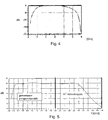
- FIG. 4 shows the frequency-dependent profile of the amplification of two series-connected narrow-band 90 ° hybrid couplers of the 11306-3 type from ANAREN XINGER.
- the narrowband 90 ° hybrid couplers operate in the frequency range of 2.0-4.0 GHz with a constant coupling factor of 3dB. Likewise, the phase stability of 90 ° is guaranteed. The gain losses in this frequency range are low. Below 2.0 GHz and above 4.0 GHz, however, the attenuation of the hybrid couplers increases sharply.
- Fig. 3 also shows that the transistor amplifier stage is suitably adapted.
- the input and output matching network of the respective transistors is realized by microstrip lines which suitably represent a combination of inductances and capacitances to obtain the desired gain curve over the entire frequency range.
- the design of a matching network is a measure familiar to a person skilled in the art.
- the transistor amplifier stage has a gain which compensates for the attenuation of the narrowband 90 ° hybrid coupler.
- the transistor amplifier stage is adapted such that in one or more predeterminable frequency ranges in which the 90 ° hybrid couplers have attenuation values greater than 3 dB, the amplification of the amplifier stages compensate for these attenuation values, such that the amplification in the frequency range of k octaves within a predefinable value range, where k ⁇ N ⁇ 0 is.
- FIG. 5 shows the frequency-dependent profile of the gain of a circuit according to the invention in FIG. 6.
- the frequency-dependent gain curve in FIG. 5 is the additive combination of the amplification characteristics illustrated in FIGS. 3 and 4.
- Fig. 5 shows that the gain curve in the frequency range of 300 MHz to 3000 MHz is 24 dB or more.
- the inventive circuit shows a constant gain over a frequency range of about 3 octaves, ie 300MHz-600MHz, 600MHz-1200MHz and 1200MHz-3200MHz.
- the circuit according to the invention has a broadband gain of 1700 MHz with 24 dB amplification. With the circuit according to the invention thus a gain of 24 dB over a frequency range of 300 MHz to 3000 MHz is possible without having to switch between individual amplifier stages.
- the circuit according to the invention is not limited to a working range of 300 MHz to 3000 MHz.
- suitable transistor amplifier stages Wide Bandgap technology enables broadband amplifier circuits with a working range from 100 MHz to 5000 MHz.
- FIG. 7 illustrates the coupling characteristic of the 90 ° hybrid coupler 1a of Fig. 6, which is 3.0 dB in its specified range of 2.0 GHz - 4.0 GHz (Anaren Xinger 11306-3 type).
- the curve a) has a coupling curve from 0 dB to -3 dB.
- the working range of the first hybrid coupler 1 a for the port A (FIG. 6) is thus between 2.0 and 4.0 GHz.
- the curve b) shows the coupling curve from -20 dB to a maximum of -3 dB.
- the working range of the second hybrid coupler 1 b for the port B is thus also between 2.0 and 4.0 GHz.
- the representation thus shows the size of the decoupled power at ports A and B.
- the consequence of using the 90 ° hybrid coupler 1a is that in the range 1. (100 MHz to 2.0 GHz) in the transistor amplifier stage 2a, also referred to as RF train, more input power is coupled to the transistor 2a as in the HF Train with transistor 2b.
- both HF trains receive the same amount of RF input power as the coupling is 3.0 dB each.
Landscapes
- Engineering & Computer Science (AREA)
- Power Engineering (AREA)
- Amplifiers (AREA)
- Microwave Amplifiers (AREA)
Applications Claiming Priority (1)
| Application Number | Priority Date | Filing Date | Title |
|---|---|---|---|
| DE102006052611A DE102006052611A1 (de) | 2006-11-08 | 2006-11-08 | Leistungsbreitbandverstärker |
Publications (2)
| Publication Number | Publication Date |
|---|---|
| EP1936802A1 true EP1936802A1 (fr) | 2008-06-25 |
| EP1936802B1 EP1936802B1 (fr) | 2011-07-13 |
Family
ID=39277475
Family Applications (1)
| Application Number | Title | Priority Date | Filing Date |
|---|---|---|---|
| EP07017833A Not-in-force EP1936802B1 (fr) | 2006-11-08 | 2007-09-12 | Amplificateur de puissance à large bande |
Country Status (4)
| Country | Link |
|---|---|
| US (1) | US7592881B2 (fr) |
| EP (1) | EP1936802B1 (fr) |
| DE (1) | DE102006052611A1 (fr) |
| ES (1) | ES2366812T3 (fr) |
Families Citing this family (8)
| Publication number | Priority date | Publication date | Assignee | Title |
|---|---|---|---|---|
| WO2011072723A1 (fr) * | 2009-12-15 | 2011-06-23 | Epcos Ag | Montage coupleur et amplificateur |
| US8918057B2 (en) * | 2010-07-26 | 2014-12-23 | Mediatek Inc. | Intelligent transmission antenna selection method and communications apparatus utilizing the same |
| US8773218B2 (en) | 2011-02-07 | 2014-07-08 | Triquint Semiconductor, Inc. | Ladder quadrature hybrid |
| WO2012118619A2 (fr) * | 2011-03-01 | 2012-09-07 | Rambus Inc. | Système de poursuite doté de polarisations orthogonales et d'une matrice à rayonnement rétrodirectif |
| US8811531B2 (en) | 2011-03-23 | 2014-08-19 | Triquint Semiconductor, Inc. | Quadrature lattice matching network |
| JP2013074070A (ja) * | 2011-09-27 | 2013-04-22 | Fujitsu Ltd | 半導体装置及び半導体装置の製造方法 |
| JP5768087B2 (ja) | 2013-05-16 | 2015-08-26 | 株式会社東芝 | 半導体電力増幅器 |
| US10686424B2 (en) * | 2015-11-12 | 2020-06-16 | Telefonaktiebolaget Lm Ericsson (Publ) | Duplexer |
Citations (10)
| Publication number | Priority date | Publication date | Assignee | Title |
|---|---|---|---|---|
| DE2807813B1 (de) * | 1978-02-23 | 1979-06-07 | Siemens Ag | Schaltungsanordnung zur Erreichung von Leistungsanpassung bei rauschangepassten Hochfrequenz-Verstaerkern |
| US4656434A (en) * | 1986-02-03 | 1987-04-07 | Raytheon Company | RF power amplifier with load mismatch compensation |
| DE3709169A1 (de) | 1987-03-20 | 1988-09-29 | Standard Elektrik Lorenz Ag | Antennenkoppler |
| JPH02111111A (ja) * | 1988-10-20 | 1990-04-24 | Sony Corp | 低雑音増幅器 |
| WO2000064048A1 (fr) * | 1999-04-16 | 2000-10-26 | Nokia Networks Oy | Amplificateur de puissance radioelectrique avec retour du port d'isolation d'un coupleur hybride |
| US6496061B1 (en) * | 2000-10-10 | 2002-12-17 | Conexant Systems, Inc. | High efficiency multiple power level amplifier |
| US20040189380A1 (en) | 2003-03-28 | 2004-09-30 | Andrew Corporation | High efficiency amplifier |
| EP1521361A1 (fr) * | 2003-10-04 | 2005-04-06 | Lucent Technologies Network Systems GmbH | Dispositif d'amplification modulaire |
| WO2005088830A1 (fr) * | 2004-03-13 | 2005-09-22 | Filtronic Plc | Amplificateur doherty |
| US20060145761A1 (en) * | 2004-12-31 | 2006-07-06 | Pribble William L | High efficiency switch-mode power amplifier |
Family Cites Families (2)
| Publication number | Priority date | Publication date | Assignee | Title |
|---|---|---|---|---|
| US3694765A (en) * | 1971-02-08 | 1972-09-26 | Bell Telephone Labor Inc | Signal coupling circuit |
| US4490684A (en) * | 1983-01-03 | 1984-12-25 | Motorola, Inc. | Adaptive quadrature combining apparatus |
-
2006
- 2006-11-08 DE DE102006052611A patent/DE102006052611A1/de not_active Withdrawn
-
2007
- 2007-09-12 ES ES07017833T patent/ES2366812T3/es active Active
- 2007-09-12 EP EP07017833A patent/EP1936802B1/fr not_active Not-in-force
- 2007-11-07 US US11/936,388 patent/US7592881B2/en not_active Expired - Fee Related
Patent Citations (10)
| Publication number | Priority date | Publication date | Assignee | Title |
|---|---|---|---|---|
| DE2807813B1 (de) * | 1978-02-23 | 1979-06-07 | Siemens Ag | Schaltungsanordnung zur Erreichung von Leistungsanpassung bei rauschangepassten Hochfrequenz-Verstaerkern |
| US4656434A (en) * | 1986-02-03 | 1987-04-07 | Raytheon Company | RF power amplifier with load mismatch compensation |
| DE3709169A1 (de) | 1987-03-20 | 1988-09-29 | Standard Elektrik Lorenz Ag | Antennenkoppler |
| JPH02111111A (ja) * | 1988-10-20 | 1990-04-24 | Sony Corp | 低雑音増幅器 |
| WO2000064048A1 (fr) * | 1999-04-16 | 2000-10-26 | Nokia Networks Oy | Amplificateur de puissance radioelectrique avec retour du port d'isolation d'un coupleur hybride |
| US6496061B1 (en) * | 2000-10-10 | 2002-12-17 | Conexant Systems, Inc. | High efficiency multiple power level amplifier |
| US20040189380A1 (en) | 2003-03-28 | 2004-09-30 | Andrew Corporation | High efficiency amplifier |
| EP1521361A1 (fr) * | 2003-10-04 | 2005-04-06 | Lucent Technologies Network Systems GmbH | Dispositif d'amplification modulaire |
| WO2005088830A1 (fr) * | 2004-03-13 | 2005-09-22 | Filtronic Plc | Amplificateur doherty |
| US20060145761A1 (en) * | 2004-12-31 | 2006-07-06 | Pribble William L | High efficiency switch-mode power amplifier |
Also Published As
| Publication number | Publication date |
|---|---|
| US20080136530A1 (en) | 2008-06-12 |
| US7592881B2 (en) | 2009-09-22 |
| DE102006052611A1 (de) | 2008-05-15 |
| EP1936802B1 (fr) | 2011-07-13 |
| ES2366812T3 (es) | 2011-10-25 |
Similar Documents
| Publication | Publication Date | Title |
|---|---|---|
| EP1936802B1 (fr) | Amplificateur de puissance à large bande | |
| EP3053265B1 (fr) | Amplificateur de puissance doherty séquentiel à large bande avec réduction de la puissance de sortie réglable | |
| DE69227574T2 (de) | Massnahmen zur Verbesserung von Verstärkern | |
| DE102007027047B4 (de) | Hochfrequenzleistungsverstärker | |
| DE69425462T2 (de) | Doherty-Mikrowellenverstärker | |
| DE102010040290B4 (de) | Richtkoppler | |
| DE112016006472T5 (de) | Lastmodulationsverstärker | |
| DE69706085T2 (de) | HEMT-HBT-Transistorkombination mit kleinem Geräusch und grosser Linearität | |
| DE102012202870A1 (de) | Breitbandige Doherty-Verstärkerschaltung | |
| DE102009036098A1 (de) | Spannungsgesteuerter Oszillator, MMIC und Hochfrequenzfunkvorrichtung | |
| DE102012216840A1 (de) | HF-Bauelement mit Ausgleichsresonatoranpassungstopologie | |
| DE102011005688A1 (de) | Halbleiterschalter, Sende-Empfangsgerät, Sender und Empfänger | |
| DE69032513T2 (de) | Verfahren und Gerät für die Breitbandimpedanzanpassung | |
| DE4037292A1 (de) | Nichtlinearitaetsgenerator mit leitfaehiger fet-source-drain-strecke und verfahren zum verstaerken eines signals | |
| DE10102891A1 (de) | Hochleistungsverstärker mit Verstärkerelement, dazugehörige Funkübertragungseinrichtung und Meßeinrichtung dafür | |
| DE69321921T2 (de) | In Kaskadenschaltung verwendbare kompakte Mikrowellenverstärkerschaltung | |
| DE102007060031B4 (de) | Halbleitervorrichtung | |
| DE112013004185B4 (de) | Richtkoppler | |
| DE112022003214T5 (de) | Doherty-Leistungsverstärker | |
| DE10100559B4 (de) | Einfachsymmetrischer Mischer | |
| DE60101089T2 (de) | Multifunktionelle integrierte schaltungsanordnung hoher frequenz | |
| DE102015209435A1 (de) | Linearisierer | |
| EP2599216B1 (fr) | Circuiterie dotée de capacités de compensation pour générer des oscillations hyperfréquence | |
| DE102008011629B4 (de) | Verstärker | |
| DE112019007905T5 (de) | Doherty-Verstärker |
Legal Events
| Date | Code | Title | Description |
|---|---|---|---|
| PUAI | Public reference made under article 153(3) epc to a published international application that has entered the european phase |
Free format text: ORIGINAL CODE: 0009012 |
|
| AK | Designated contracting states |
Kind code of ref document: A1 Designated state(s): AT BE BG CH CY CZ DE DK EE ES FI FR GB GR HU IE IS IT LI LT LU LV MC MT NL PL PT RO SE SI SK TR |
|
| AX | Request for extension of the european patent |
Extension state: AL BA HR MK RS |
|
| 17P | Request for examination filed |
Effective date: 20080718 |
|
| AKX | Designation fees paid |
Designated state(s): DE ES FR GB IT |
|
| GRAP | Despatch of communication of intention to grant a patent |
Free format text: ORIGINAL CODE: EPIDOSNIGR1 |
|
| GRAS | Grant fee paid |
Free format text: ORIGINAL CODE: EPIDOSNIGR3 |
|
| GRAA | (expected) grant |
Free format text: ORIGINAL CODE: 0009210 |
|
| AK | Designated contracting states |
Kind code of ref document: B1 Designated state(s): DE ES FR GB IT |
|
| REG | Reference to a national code |
Ref country code: GB Ref legal event code: FG4D Free format text: NOT ENGLISH |
|
| REG | Reference to a national code |
Ref country code: DE Ref legal event code: R096 Ref document number: 502007007643 Country of ref document: DE Effective date: 20110908 |
|
| REG | Reference to a national code |
Ref country code: ES Ref legal event code: FG2A Ref document number: 2366812 Country of ref document: ES Kind code of ref document: T3 Effective date: 20111025 |
|
| PLBE | No opposition filed within time limit |
Free format text: ORIGINAL CODE: 0009261 |
|
| STAA | Information on the status of an ep patent application or granted ep patent |
Free format text: STATUS: NO OPPOSITION FILED WITHIN TIME LIMIT |
|
| 26N | No opposition filed |
Effective date: 20120416 |
|
| REG | Reference to a national code |
Ref country code: DE Ref legal event code: R097 Ref document number: 502007007643 Country of ref document: DE Effective date: 20120416 |
|
| PGFP | Annual fee paid to national office [announced via postgrant information from national office to epo] |
Ref country code: ES Payment date: 20130927 Year of fee payment: 7 |
|
| REG | Reference to a national code |
Ref country code: DE Ref legal event code: R081 Ref document number: 502007007643 Country of ref document: DE Owner name: AIRBUS DS ELECTRONICS AND BORDER SECURITY GMBH, DE Free format text: FORMER OWNER: EADS DEUTSCHLAND GMBH, 85521 OTTOBRUNN, DE Effective date: 20140916 Ref country code: DE Ref legal event code: R081 Ref document number: 502007007643 Country of ref document: DE Owner name: AIRBUS DEFENCE AND SPACE GMBH, DE Free format text: FORMER OWNER: EADS DEUTSCHLAND GMBH, 85521 OTTOBRUNN, DE Effective date: 20140916 Ref country code: DE Ref legal event code: R081 Ref document number: 502007007643 Country of ref document: DE Owner name: HENSOLDT SENSORS GMBH, DE Free format text: FORMER OWNER: EADS DEUTSCHLAND GMBH, 85521 OTTOBRUNN, DE Effective date: 20140916 |
|
| REG | Reference to a national code |
Ref country code: FR Ref legal event code: PLFP Year of fee payment: 9 |
|
| REG | Reference to a national code |
Ref country code: ES Ref legal event code: FD2A Effective date: 20160205 |
|
| PG25 | Lapsed in a contracting state [announced via postgrant information from national office to epo] |
Ref country code: ES Free format text: LAPSE BECAUSE OF NON-PAYMENT OF DUE FEES Effective date: 20140913 |
|
| REG | Reference to a national code |
Ref country code: DE Ref legal event code: R081 Ref document number: 502007007643 Country of ref document: DE Owner name: AIRBUS DS ELECTRONICS AND BORDER SECURITY GMBH, DE Free format text: FORMER OWNER: AIRBUS DEFENCE AND SPACE GMBH, 85521 OTTOBRUNN, DE Ref country code: DE Ref legal event code: R081 Ref document number: 502007007643 Country of ref document: DE Owner name: HENSOLDT SENSORS GMBH, DE Free format text: FORMER OWNER: AIRBUS DEFENCE AND SPACE GMBH, 85521 OTTOBRUNN, DE |
|
| REG | Reference to a national code |
Ref country code: FR Ref legal event code: PLFP Year of fee payment: 10 |
|
| PGFP | Annual fee paid to national office [announced via postgrant information from national office to epo] |
Ref country code: GB Payment date: 20160920 Year of fee payment: 10 Ref country code: DE Payment date: 20160921 Year of fee payment: 10 |
|
| PGFP | Annual fee paid to national office [announced via postgrant information from national office to epo] |
Ref country code: FR Payment date: 20160921 Year of fee payment: 10 |
|
| PGFP | Annual fee paid to national office [announced via postgrant information from national office to epo] |
Ref country code: IT Payment date: 20160922 Year of fee payment: 10 |
|
| REG | Reference to a national code |
Ref country code: DE Ref legal event code: R082 Ref document number: 502007007643 Country of ref document: DE Representative=s name: LIFETECH IP SPIES & BEHRNDT PATENTANWAELTE PAR, DE Ref country code: DE Ref legal event code: R081 Ref document number: 502007007643 Country of ref document: DE Owner name: HENSOLDT SENSORS GMBH, DE Free format text: FORMER OWNER: AIRBUS DS ELECTRONICS AND BORDER SECURITY GMBH, 82024 TAUFKIRCHEN, DE |
|
| REG | Reference to a national code |
Ref country code: DE Ref legal event code: R119 Ref document number: 502007007643 Country of ref document: DE |
|
| GBPC | Gb: european patent ceased through non-payment of renewal fee |
Effective date: 20170912 |
|
| REG | Reference to a national code |
Ref country code: FR Ref legal event code: ST Effective date: 20180531 |
|
| PG25 | Lapsed in a contracting state [announced via postgrant information from national office to epo] |
Ref country code: GB Free format text: LAPSE BECAUSE OF NON-PAYMENT OF DUE FEES Effective date: 20170912 Ref country code: DE Free format text: LAPSE BECAUSE OF NON-PAYMENT OF DUE FEES Effective date: 20180404 |
|
| PG25 | Lapsed in a contracting state [announced via postgrant information from national office to epo] |
Ref country code: IT Free format text: LAPSE BECAUSE OF NON-PAYMENT OF DUE FEES Effective date: 20170912 Ref country code: FR Free format text: LAPSE BECAUSE OF NON-PAYMENT OF DUE FEES Effective date: 20171002 |