EP1939792A1 - Verfahren zur Umsetzung von Vorrichtungen zur Hochfrequenzkommunikation mit oder ohne Funktionsschalter und erhaltene Vorrichtungen - Google Patents
Verfahren zur Umsetzung von Vorrichtungen zur Hochfrequenzkommunikation mit oder ohne Funktionsschalter und erhaltene Vorrichtungen Download PDFInfo
- Publication number
- EP1939792A1 EP1939792A1 EP06301302A EP06301302A EP1939792A1 EP 1939792 A1 EP1939792 A1 EP 1939792A1 EP 06301302 A EP06301302 A EP 06301302A EP 06301302 A EP06301302 A EP 06301302A EP 1939792 A1 EP1939792 A1 EP 1939792A1
- Authority
- EP
- European Patent Office
- Prior art keywords
- antenna
- circuit
- switch
- cavity
- electronic component
- Prior art date
- Legal status (The legal status is an assumption and is not a legal conclusion. Google has not performed a legal analysis and makes no representation as to the accuracy of the status listed.)
- Withdrawn
Links
Images
Classifications
-
- H—ELECTRICITY
- H01—ELECTRIC ELEMENTS
- H01Q—ANTENNAS, i.e. RADIO AERIALS
- H01Q7/00—Loop antennas with a substantially uniform current distribution around the loop and having a directional radiation pattern in a plane perpendicular to the plane of the loop
-
- G—PHYSICS
- G06—COMPUTING OR CALCULATING; COUNTING
- G06K—GRAPHICAL DATA READING; PRESENTATION OF DATA; RECORD CARRIERS; HANDLING RECORD CARRIERS
- G06K19/00—Record carriers for use with machines and with at least a part designed to carry digital markings
- G06K19/06—Record carriers for use with machines and with at least a part designed to carry digital markings characterised by the kind of the digital marking, e.g. shape, nature, code
- G06K19/067—Record carriers with conductive marks, printed circuits or semiconductor circuit elements, e.g. credit or identity cards also with resonating or responding marks without active components
- G06K19/07—Record carriers with conductive marks, printed circuits or semiconductor circuit elements, e.g. credit or identity cards also with resonating or responding marks without active components with integrated circuit chips
- G06K19/073—Special arrangements for circuits, e.g. for protecting identification code in memory
- G06K19/07309—Means for preventing undesired reading or writing from or onto record carriers
- G06K19/07345—Means for preventing undesired reading or writing from or onto record carriers by activating or deactivating at least a part of the circuit on the record carrier, e.g. ON/OFF switches
-
- H—ELECTRICITY
- H01—ELECTRIC ELEMENTS
- H01H—ELECTRIC SWITCHES; RELAYS; SELECTORS; EMERGENCY PROTECTIVE DEVICES
- H01H13/00—Switches having rectilinearly-movable operating part or parts adapted for pushing or pulling in one direction only, e.g. push-button switch
- H01H13/70—Switches having rectilinearly-movable operating part or parts adapted for pushing or pulling in one direction only, e.g. push-button switch having a plurality of operating members associated with different sets of contacts, e.g. keyboard
- H01H13/88—Processes specially adapted for manufacture of rectilinearly movable switches having a plurality of operating members associated with different sets of contacts, e.g. keyboards
-
- H—ELECTRICITY
- H01—ELECTRIC ELEMENTS
- H01Q—ANTENNAS, i.e. RADIO AERIALS
- H01Q1/00—Details of, or arrangements associated with, antennas
- H01Q1/12—Supports; Mounting means
- H01Q1/22—Supports; Mounting means by structural association with other equipment or articles
-
- H—ELECTRICITY
- H01—ELECTRIC ELEMENTS
- H01Q—ANTENNAS, i.e. RADIO AERIALS
- H01Q1/00—Details of, or arrangements associated with, antennas
- H01Q1/12—Supports; Mounting means
- H01Q1/22—Supports; Mounting means by structural association with other equipment or articles
- H01Q1/2208—Supports; Mounting means by structural association with other equipment or articles associated with components used in interrogation type services, i.e. in systems for information exchange between an interrogator/reader and a tag/transponder, e.g. in Radio Frequency Identification [RFID] systems
- H01Q1/2225—Supports; Mounting means by structural association with other equipment or articles associated with components used in interrogation type services, i.e. in systems for information exchange between an interrogator/reader and a tag/transponder, e.g. in Radio Frequency Identification [RFID] systems used in active tags, i.e. provided with its own power source or in passive tags, i.e. deriving power from RF signal
-
- H—ELECTRICITY
- H01—ELECTRIC ELEMENTS
- H01Q—ANTENNAS, i.e. RADIO AERIALS
- H01Q1/00—Details of, or arrangements associated with, antennas
- H01Q1/40—Radiating elements coated with or embedded in protective material
-
- H—ELECTRICITY
- H01—ELECTRIC ELEMENTS
- H01H—ELECTRIC SWITCHES; RELAYS; SELECTORS; EMERGENCY PROTECTIVE DEVICES
- H01H2203/00—Form of contacts
- H01H2203/036—Form of contacts to solve particular problems
- H01H2203/038—Form of contacts to solve particular problems to be bridged by a dome shaped contact
-
- H—ELECTRICITY
- H01—ELECTRIC ELEMENTS
- H01H—ELECTRIC SWITCHES; RELAYS; SELECTORS; EMERGENCY PROTECTIVE DEVICES
- H01H2205/00—Movable contacts
- H01H2205/016—Separate bridge contact
- H01H2205/024—Means to facilitate positioning
- H01H2205/03—Apertured plate
-
- H—ELECTRICITY
- H01—ELECTRIC ELEMENTS
- H01H—ELECTRIC SWITCHES; RELAYS; SELECTORS; EMERGENCY PROTECTIVE DEVICES
- H01H2231/00—Applications
- H01H2231/05—Card, e.g. credit card
Definitions
- the invention relates to a method for producing radiofrequency communication devices with or without a switch preventing the device from being read without the knowledge of the wearer, as well as the devices obtained.
- the devices referred to in the first place by the invention are contactless or hybrid type smart cards, inserts comprising a radiofrequency antenna, where appropriate for any antenna circuit support such as electronic passports.
- radio frequency communication devices known as transponders, for the most part meet the ISO-IEC 14443 standard.
- This device is intended to provide the carrier of the transponder with means for accepting and / or refusing access to data contained in said transponder to an external reading device.
- Such conductive wires generally made of copper, which are very thin, of the order of 113 ⁇ m, and spaced on the order of 700 ⁇ m to constitute antenna turns, make it possible to obtain a high quality factor, for example greater than 44 unlike antennas obtained by deposition of conductive material, in particular by screen printing conductive ink.
- the diameter of the turns may be between 200 microns to 300 microns.
- the second disadvantage of the process used today in button cards is the change of the course or arrangement of the antenna equipped with an open circuit portion to accommodate the button.
- the current method does not allow to test the operation of the card before the addition of the button. In addition, it imposes on us a new arrangement of antenna turns, a new product and therefore new constraints of stock management.
- the object of the invention is to solve the aforementioned drawbacks and to allow more flexibility in the production and the functional test.
- the invention consists in its principle to add in series at the antenna, a conductive loop or circuit portion at a distance from normal or regular turns; thus it is possible to have cards or inserts usable either with means of inhibition / authorization in the form of a button, or as simple standard contactless cards.
- the solution proposed here offers the advantage of using a button with all the current technologies of manufacture of contactless insert or ("inlay" in English terminology).
- the solution is compatible with standard smart card manufacturing processes.
- This manufacturing method has the advantage of using common inserts for device with or without switch. It also makes it possible to electrically test the insert or to load data into the insert at a very advanced stage in the manufacture of the device. While in the prior art, it is necessary to wait for the button and press it to allow operation.
- the subject of the invention is also an electronic radiofrequency communication device comprising an electronic component, a an antenna electrical circuit connected to the electronic component and a switch disposed on the antenna circuit and adapted to close the antenna circuit by actuation;
- the device is distinguished in that it comprises an interruption zone of the antenna circuit made by removing material from the antenna.
- This radiofrequency communication device structure with switch results from the implementation of the method of the invention.
- the device comprises in particular at the switch traces of removal of material from the antenna for producing an open circuit.
- the invention also relates to a device having a support and a closed antenna circuit having turns with two connection ends for connection to an electronic component, arranged on the support, with a regular inter-turn spacing; It is distinguished in that the antenna has a turn portion longer than 10 mm extending entirely at a distance of at least 10 mm from its regular coil path and connection ends to an electronic component.
- This structure has the advantage of being suitable for producing a common antenna support that can be used with or without a switch, the preferred dimensions of which are of the order of 10 mm in width or in diameter.
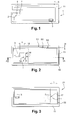
- the embodiment according to the prior art of a radiofrequency communication device or transponder 1 which comprises an electronic component 3, an antenna circuit 5 associated with the electronic component 3 and a reception zone Z of a switch on the circuit capable of closing the antenna circuit, open at this level.
- the antenna circuit comprises as soon as it is made on a support 11 two openings, respectively for the connection to the electronic component and to interact with a switch (not shown).
- Contact pads or pads 7, 9 are provided on the antenna coil at the location of the switch.
- This device has the disadvantage of not being able to operate in an intermediate state that would not include a switch closing the circuit at the contacts 7 and 8 and allowing operation.
- the figure 2 illustrates a radiofrequency device in the form of an insert for a contactless smart card obtained by an embodiment of the method of the invention.
- the method comprises a first step in which the antenna 13 is in the form of a closed circuit (with the exception of the antenna ends connected to the electronic component).
- the antenna 13 is at least closed circuit at a zone (I) able to receive a switch.
- the antenna has 3 turns S1, S2, S3, having a regular spacing (e) determined to 700 microns.
- regular spacing means a substantially constant spacing between the turns.
- the turns together form a coil having a regular path with an inter-turn spacing less than or equal to 2 mm or 3.5 mm.
- the turns have for example a diameter of between 50 to 300 microns and are sheathed with insulation.
- the turns are generally arranged parallel and spaced regularly relative to each other but it is not excluded to have substantially variable spacings).
- the wire is embedded in a polymeric support 11 by ultra sounds. But it could be achieved otherwise, by any known technique, such as etching and electrochemical deposition, metal sheet cutting.
- the support may be in various materials including synthetic and / or comprise fibers of cellulosic material such as paper.
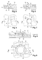
- the antenna comprises a portion 15 located at a distance from the turns and which does not follow a normal or regular course formed by the other turns.
- the portion 15 deviates from the normal path obviously for no apparent reason, unlike, for example, connecting a component.
- This antenna portion is in the example located outside of its regular path forming the coil and located in particular at the periphery of the support.
- the portion 15 is spaced both from its regular path and from the connection ends by a distance D.
- This distance D is preferably greater than 10 mm, or even more than 15 mm or 20 mm. But it could be smaller depending on the size of the switch, for example 5 to 10 mm.
- the continuous and closed portion of the coil has a length (L) of more than 10 mm and is entirely removed from its inter-turn spacing (e).
- e inter-turn spacing
- a portion of more than 20 mm antenna turn is derived from the normal coil path as a loop or a "U”.
- the card has the ISO format of 54 mm X 76 mm.
- the portion 15 may comprise two branches (54, 56) facing one another, for example in the shape of "U” or “V” and distant from a length of between 1 and 10 mm depending on the width of the conductive element 19 of the switch.
- the antenna is substantially rectangular with a small side 22 and the antenna portion 17 is parallel to this small side and extends transversely in the full surface of the support 11 at a distance D from the side edge.
- the dotted circle illustrates a zone location (I) for receiving the switch or being machined.
- an interruption zone of the antenna circuit is created on the antenna circuit portion 17 at least by removal of material from the antenna.
- the antenna is necessary that the antenna at least is cut completely.
- the antenna material is preferably removed with carrier material located below.
- the component in the example comprises an integrated circuit connected to the antenna.
- the material is removed after provision of a protective or coating layer 24 on the antenna circuit and the component 3.
- a first machining of a cavity 26 is carried out through the cover sheet so as to create a cavity bottom 28 below said portion or antenna plane until the portion of the cavity is completely cut off.
- the method further comprises producing a second cavity machining 34 wider than the first 26 so as to discover at the surface the two free conductive ends of said antenna portion and have contact zones 36, 38 oriented towards the outside of the cavity.
- This second machining is less deep, it just radially deny the turns at this level, and therefore they each have a bare surface 36, 38 facing the entrance of the cavity.
- the conductive material 40 is preferably disposed on the antenna turn parts thus discovered and machined 36, 38 so as, on the one hand, to facilitate electrical contact with a short-circuit element of the switch. by an extra thickness, but also possibly avoid oxidation or corrosion, which would prevent a good electrical contact.
- the material is preferably elastic at room temperature to dampen contact with the switch and facilitate contacts. It may comprise for example a conductive polymer.
- a switch 42 is interposed on the antenna circuit in the receiving zone of the switch so as to close the antenna circuit.
- a short-circuit conducting elastic element 19 is interposed so as to short-circuit or bring into contact said two free conductive ends 30, 32, under the effect of an actuation, or exercise of a pressure P on the element 19.
- the element here is a Belleville type washer, having a central dome 46, connected to four feet 48 in the form of an elastic tongue.
- the feet rest on the plane 50 of the second machining, and under the effect of pressure, the tongues deform elastically and the dome in sagging short circuit or in electrical contact the two free ends 30, 32 exposed in the cavity.
- a flexible cover or membrane 52 accessible from the outside, is fixed, in particular by gluing, on a third plane 54 machined above the conductive element, by closing the cavity.
- the antenna comprises, in the switch zone, the turns arranged in particular by embroidery above the surface of its support, for example fibrous or woven. Then, there is a cover sheet already having a cavity over the antenna so that the contacts 30, 32 are located in the cavity. If necessary, the sheet could already include the diaphragm or cover and / or a short-circuit element, which would facilitate the assembly of the antenna support part with a support part of interruption or short-circuit means .
- the device, the card or insert is automatically made with the button covering a closed or continuous circuit portion and an opening of the circuit is made, for example, by drilling via the rear face opposite to that with the button.
- a final covering sheet closes the orifice thus created.
- the cutting of the antenna can be achieved by a first button press.
- the button would include means for cutting the circuit at a weakened position beforehand; for example, the circuit may be devoid of support very locally at the weakened location (for example, on 2 X 2 mm), in particular by forming a bridge over a perforation of the support.
- the button could include a rod or blade slidable in the perforation to sever the circuit.
- the opening step can be performed in the switch area; However, it can be carried out outside this zone, for example by a pre-cut in the support or outside a finished or standardized surface of the support, waiting for cutting by pressure of fingers or other means, the portion may extend for example to the edge of the device, or a corner or beyond an edge to be final.
- the advantage of these two embodiments is to allow a test operation as late as possible including until the first use of the device.
- the radiofrequency electronic communication device obtained comprises an interruption zone of the antenna circuit made by removing material from the antenna.
- it is a contactless bank card.
- it could be an insert for passport or ID card or whatever.
- the radiofrequency electronic communication device obtained comprises a first cavity 26 with a bottom 28 which extends through at least one cover sheet 24; The bottom is disposed below said antenna portion or an antenna plane.
- the two free ends 30, 32 of contact of the antenna open into the cavity and each have a substantially transverse or oblique section 42, 44 flush with the inner wall 26 of the cavity.
- the ends have the same profile as the cavity and in this case circular or cylindrical.
- the intersection of the son with the cavity is here a cylindrical surface. It can be plane if the intersection corresponds to a plane (case of a parallelepipedic cavity).
- the device of the invention of Figures 2 or 3 can be used for two uses with or without switch; the insert comprises on a support 15, a closed antenna circuit with turns having two connection ends for connection to an electronic component.
- connection of the component may be performed on the insert 21 and this insert can be used as well or may undergo other finishing steps such as a lamination of cover sheets and / or decoration 42 to form a contactless smart card to antenna or even contact-type and contact-free with a specific module having contact pads flush with the surface of the card body in addition to the connection contacts, to the antenna.
- the invention can be applied to any conducting circuit in which the circuit is opened mechanically at the location of the switch after completion of the circuit continuously at this point.
- the circuit can form something other than an antenna coil, or antenna connection track.
- the loop end is in the cavity but in a variant, this end could be located outside the cavity or the switch zone, or even outside the standard surface of the card. Therefore the loop would be open at a distance from the switch.
- the interruption zone is located outside the switch area in which two strands (54, 56) circuit arranged to cooperate with the switch.
Landscapes
- Engineering & Computer Science (AREA)
- Computer Hardware Design (AREA)
- Computer Security & Cryptography (AREA)
- General Engineering & Computer Science (AREA)
- Microelectronics & Electronic Packaging (AREA)
- Physics & Mathematics (AREA)
- General Physics & Mathematics (AREA)
- Theoretical Computer Science (AREA)
- Details Of Aerials (AREA)
- Credit Cards Or The Like (AREA)
Priority Applications (4)
| Application Number | Priority Date | Filing Date | Title |
|---|---|---|---|
| EP06301302A EP1939792A1 (de) | 2006-12-28 | 2006-12-28 | Verfahren zur Umsetzung von Vorrichtungen zur Hochfrequenzkommunikation mit oder ohne Funktionsschalter und erhaltene Vorrichtungen |
| US12/521,499 US9705191B2 (en) | 2006-12-28 | 2007-12-20 | Method for producing radiofrequency communication devices with or without operation switch and devices thus obtained |
| EP07857938A EP2132683A1 (de) | 2006-12-28 | 2007-12-20 | Verfahren zum herstellen von hochfrequenz-kommunikationsgeräten mit oder ohne betriebsschalter und so erhaltene geräte |
| PCT/EP2007/064317 WO2008080876A1 (fr) | 2006-12-28 | 2007-12-20 | Procede de realisation de dispositifs de communication radiofrequence avec ou sans interrupteur de fonctionnement et dispositifs obtenus |
Applications Claiming Priority (1)
| Application Number | Priority Date | Filing Date | Title |
|---|---|---|---|
| EP06301302A EP1939792A1 (de) | 2006-12-28 | 2006-12-28 | Verfahren zur Umsetzung von Vorrichtungen zur Hochfrequenzkommunikation mit oder ohne Funktionsschalter und erhaltene Vorrichtungen |
Publications (1)
| Publication Number | Publication Date |
|---|---|
| EP1939792A1 true EP1939792A1 (de) | 2008-07-02 |
Family
ID=38055382
Family Applications (2)
| Application Number | Title | Priority Date | Filing Date |
|---|---|---|---|
| EP06301302A Withdrawn EP1939792A1 (de) | 2006-12-28 | 2006-12-28 | Verfahren zur Umsetzung von Vorrichtungen zur Hochfrequenzkommunikation mit oder ohne Funktionsschalter und erhaltene Vorrichtungen |
| EP07857938A Withdrawn EP2132683A1 (de) | 2006-12-28 | 2007-12-20 | Verfahren zum herstellen von hochfrequenz-kommunikationsgeräten mit oder ohne betriebsschalter und so erhaltene geräte |
Family Applications After (1)
| Application Number | Title | Priority Date | Filing Date |
|---|---|---|---|
| EP07857938A Withdrawn EP2132683A1 (de) | 2006-12-28 | 2007-12-20 | Verfahren zum herstellen von hochfrequenz-kommunikationsgeräten mit oder ohne betriebsschalter und so erhaltene geräte |
Country Status (3)
| Country | Link |
|---|---|
| US (1) | US9705191B2 (de) |
| EP (2) | EP1939792A1 (de) |
| WO (1) | WO2008080876A1 (de) |
Cited By (3)
| Publication number | Priority date | Publication date | Assignee | Title |
|---|---|---|---|---|
| FR2949639A1 (fr) * | 2009-09-03 | 2011-03-04 | Oberthur Technologies | Procede de fabrication d'une carte incorporant un commutateur |
| WO2013072578A1 (fr) | 2011-11-15 | 2013-05-23 | Ask S.A. | Dispositif de communication radiofréquence dont le fonctionnement est contrôlé par un geste volontaire du porteur |
| EP2743952A1 (de) * | 2012-12-17 | 2014-06-18 | Oberthur Technologies | Kontaktgeber für dünne Plastikkarte |
Families Citing this family (5)
| Publication number | Priority date | Publication date | Assignee | Title |
|---|---|---|---|---|
| AT515401B1 (de) * | 2014-02-03 | 2016-04-15 | Seibersdorf Labor Gmbh | Abschirmelement zum Anbringen auf einem Gegenstand |
| CN104978593A (zh) * | 2014-04-02 | 2015-10-14 | 北京数码视讯科技股份有限公司 | 一种电子支付方法和非接触ic卡 |
| EP3166181A1 (de) * | 2015-11-05 | 2017-05-10 | Gemalto Sa | Herstellungsverfahren einer funkantenne auf einer halterung, und so erhaltene antenne |
| ES2770756T3 (es) * | 2017-01-11 | 2020-07-03 | Asef Mohammad Khaled | Pulsador de doble cara con función táctil |
| KR20220031640A (ko) * | 2019-07-26 | 2022-03-11 | 코나아이 (주) | 나무 시트가 포함된 카드 및 그 제조 방법 |
Citations (3)
| Publication number | Priority date | Publication date | Assignee | Title |
|---|---|---|---|---|
| DE10140662C1 (de) * | 2001-08-24 | 2003-03-20 | Orga Kartensysteme Gmbh | Chipkarte mit integriertem Schalter |
| EP1544787A1 (de) * | 2003-12-19 | 2005-06-22 | Axalto SA | Kontaktlose Karte mit einem Antennenschalter |
| DE102005020092A1 (de) * | 2005-04-29 | 2006-11-16 | Giesecke & Devrient Gmbh | Verfahren zur Herstellung eines tragbaren Datenträgers |
Family Cites Families (11)
| Publication number | Priority date | Publication date | Assignee | Title |
|---|---|---|---|---|
| US6268796B1 (en) * | 1997-12-12 | 2001-07-31 | Alfred Gnadinger | Radio frequency identification transponder having integrated antenna |
| US7586397B2 (en) * | 1999-05-06 | 2009-09-08 | Vulcan Patents Llc | Interactive radio frequency tags |
| WO2001040915A2 (en) * | 1999-12-06 | 2001-06-07 | Avery Dennison Corporation | Digital binder and method therefor |
| WO2003030300A1 (en) * | 2001-09-28 | 2003-04-10 | Mitsubishi Materials Corporation | Antenna coil and rfid-use tag using it, transponder-use antenna |
| JP4238221B2 (ja) * | 2003-01-23 | 2009-03-18 | バクームシュメルツェ ゲゼルシャフト ミット ベシュレンクテル ハフツング ウント コンパニ コマンディートゲゼルシャフト | アンテナコア |
| US7151455B2 (en) * | 2004-04-30 | 2006-12-19 | Kimberly-Clark Worldwide, Inc. | Activating a data tag by load or orientation or user control |
| DE102005036303A1 (de) * | 2005-04-29 | 2007-08-16 | Giesecke & Devrient Gmbh | Verfahren zur Initialisierung und/oder Personalisierung eines tragbaren Datenträgers |
| US7503491B2 (en) * | 2005-10-29 | 2009-03-17 | Magnex Corporation | RFID chip and antenna with improved range |
| IL175824A0 (en) * | 2006-05-22 | 2007-09-20 | On Track Innovations Ltd | Data transaction card having a tunable coil antenna with reduced footprint |
| US20070290856A1 (en) * | 2006-06-19 | 2007-12-20 | Tagsys Sas | RFID tag detuning |
| US8608080B2 (en) * | 2006-09-26 | 2013-12-17 | Feinics Amatech Teoranta | Inlays for security documents |
-
2006
- 2006-12-28 EP EP06301302A patent/EP1939792A1/de not_active Withdrawn
-
2007
- 2007-12-20 EP EP07857938A patent/EP2132683A1/de not_active Withdrawn
- 2007-12-20 WO PCT/EP2007/064317 patent/WO2008080876A1/fr not_active Ceased
- 2007-12-20 US US12/521,499 patent/US9705191B2/en not_active Expired - Fee Related
Patent Citations (3)
| Publication number | Priority date | Publication date | Assignee | Title |
|---|---|---|---|---|
| DE10140662C1 (de) * | 2001-08-24 | 2003-03-20 | Orga Kartensysteme Gmbh | Chipkarte mit integriertem Schalter |
| EP1544787A1 (de) * | 2003-12-19 | 2005-06-22 | Axalto SA | Kontaktlose Karte mit einem Antennenschalter |
| DE102005020092A1 (de) * | 2005-04-29 | 2006-11-16 | Giesecke & Devrient Gmbh | Verfahren zur Herstellung eines tragbaren Datenträgers |
Cited By (5)
| Publication number | Priority date | Publication date | Assignee | Title |
|---|---|---|---|---|
| FR2949639A1 (fr) * | 2009-09-03 | 2011-03-04 | Oberthur Technologies | Procede de fabrication d'une carte incorporant un commutateur |
| WO2013072578A1 (fr) | 2011-11-15 | 2013-05-23 | Ask S.A. | Dispositif de communication radiofréquence dont le fonctionnement est contrôlé par un geste volontaire du porteur |
| EP2743952A1 (de) * | 2012-12-17 | 2014-06-18 | Oberthur Technologies | Kontaktgeber für dünne Plastikkarte |
| FR2999784A1 (fr) * | 2012-12-17 | 2014-06-20 | Oberthur Technologies | Contacteur pour carte plastique mince |
| EP2743952B1 (de) | 2012-12-17 | 2015-09-16 | Oberthur Technologies | Kontaktgeber für dünne Plastikkarte |
Also Published As
| Publication number | Publication date |
|---|---|
| US20100197245A1 (en) | 2010-08-05 |
| EP2132683A1 (de) | 2009-12-16 |
| WO2008080876A1 (fr) | 2008-07-10 |
| US9705191B2 (en) | 2017-07-11 |
Similar Documents
| Publication | Publication Date | Title |
|---|---|---|
| EP2132683A1 (de) | Verfahren zum herstellen von hochfrequenz-kommunikationsgeräten mit oder ohne betriebsschalter und so erhaltene geräte | |
| EP2218040B1 (de) | Hochfrequenzkommunikationseinrichtung mit einem timer | |
| EP1932104B1 (de) | Doppelschnittstellen-kommunikations-elektronikmodul insbesondere für eine chipkarte | |
| EP3201842B1 (de) | Elektronisches dokument mit abgewinkelten antennenenden, antennenhalter für solch ein elektronisches dokument sowie verfahren zur herstellung solch eines dokuments | |
| EP2867831B1 (de) | Verfahren zur herstellung eines kontaktlosen mikrochips | |
| FR2716281A1 (fr) | Procédé de fabrication d'une carte sans contact. | |
| EP2710522B1 (de) | Vorrichtung mit einem drahtkondensator insbesondere für eine radiofrequenzschaltung | |
| EP1185955B1 (de) | Laminierherstellungsverfahren einer kontaktlosen karte | |
| EP2002384B1 (de) | Hochfrequenzanordnung | |
| EP2545503B1 (de) | Elektronische vorrichtung mit einem chip und herstellungsverfahren mittels spulen | |
| EP3899792B1 (de) | Herstellungsverfahren einer metallischen funkfrequenz-chipkarte mit verbesserter elektromagnetischer leitfähigkeit | |
| EP2045765B1 (de) | Verfahren zur Herstellung eines elektronischen Schlüssels mit USB-Stecker | |
| EP2053545A1 (de) | Verfahren zur Herstellung von Funkkommunikationsvorrichtungen, die einen vorübergehend kurzgeschlossenen Schalter umfassen | |
| EP2915104B1 (de) | Verfahren zur herstellung einer anschlussvorrichtung für das modul einer smart card, durch das verfahren erhaltene anschlussvorrichtung und modul mit smart card anschlussvorrichtung | |
| EP3671564A1 (de) | Herstellungsverfahren eines einsatzes einer funkfrequenz-chipkarte, der eine metallplatte umfasst | |
| EP1955258A1 (de) | Verfahren zum herstellen eines kontaktlosen transponders durch aufheften des kontaktlosen moduls auf eine antenne und erhaltener transponder | |
| WO2020114753A1 (fr) | Procede de fabrication d'une carte a puce metallique ou non avec antenne relais | |
| EP2800461B1 (de) | Herstellungsverfahren eines flexiblen Schaltkreises für Chipkartenmodul, mit diesem Verfahren hergestellter flexibler Schaltkreis für Chipkartenmodul und Chipkartenmodul, das einen solchen flexiblen Schaltkreis umfasst | |
| FR2938380A1 (fr) | Couche support d'antenne filaire et/ou d'elements de connexion filaire pour carte a microcircuit | |
| WO2020126572A1 (fr) | Procede de fabrication d'une carte a puce metallique, de preference avec antenne relais | |
| FR2999753A1 (fr) | Procede de fabrication par lamination en continu de cartes a microcircuit du type a contact | |
| EP3496005A1 (de) | Herstellungsverfahren eines trägers mit funkfrequenz-chip | |
| WO2020127109A1 (fr) | Procede de fabrication d'une carte a puce radiofrequence metallique a permittivite amelioree avec perforations etendues | |
| EP2525305A1 (de) | Fadenkondensator, insbesondere für Funkschaltkreis, und diesen umfassende Vorrichtung | |
| FR2794267A1 (fr) | Dispositif portable a circuit integre, de type carte a puce de format reduit par rapport au format standard des cartes a puces et procede de fabrication |
Legal Events
| Date | Code | Title | Description |
|---|---|---|---|
| PUAI | Public reference made under article 153(3) epc to a published international application that has entered the european phase |
Free format text: ORIGINAL CODE: 0009012 |
|
| AK | Designated contracting states |
Kind code of ref document: A1 Designated state(s): AT BE BG CH CY CZ DE DK EE ES FI FR GB GR HU IE IS IT LI LT LU LV MC NL PL PT RO SE SI SK TR |
|
| AX | Request for extension of the european patent |
Extension state: AL BA HR MK RS |
|
| 17P | Request for examination filed |
Effective date: 20090105 |
|
| AKX | Designation fees paid |
Designated state(s): AT BE BG CH CY CZ DE DK EE ES FI FR GB GR HU IE IS IT LI LT LU LV MC NL PL PT RO SE SI SK TR |
|
| STAA | Information on the status of an ep patent application or granted ep patent |
Free format text: STATUS: THE APPLICATION IS DEEMED TO BE WITHDRAWN |
|
| 18D | Application deemed to be withdrawn |
Effective date: 20090106 |
|
| D17P | Request for examination filed (deleted) | ||
| DBV | Designated contracting states (deleted) |