EP1939917A2 - Photocathode, tube photomultiplicateur et tube d'électron - Google Patents
Photocathode, tube photomultiplicateur et tube d'électron Download PDFInfo
- Publication number
- EP1939917A2 EP1939917A2 EP07024966A EP07024966A EP1939917A2 EP 1939917 A2 EP1939917 A2 EP 1939917A2 EP 07024966 A EP07024966 A EP 07024966A EP 07024966 A EP07024966 A EP 07024966A EP 1939917 A2 EP1939917 A2 EP 1939917A2
- Authority
- EP
- European Patent Office
- Prior art keywords
- photocathode
- photoelectron emitting
- emitting layer
- underlayer
- supporting substrate
- Prior art date
- Legal status (The legal status is an assumption and is not a legal conclusion. Google has not performed a legal analysis and makes no representation as to the accuracy of the status listed.)
- Granted
Links
Images



Classifications
-
- H—ELECTRICITY
- H01—ELECTRIC ELEMENTS
- H01J—ELECTRIC DISCHARGE TUBES OR DISCHARGE LAMPS
- H01J1/00—Details of electrodes, of magnetic control means, of screens, or of the mounting or spacing thereof, common to two or more basic types of discharge tubes or lamps
- H01J1/02—Main electrodes
- H01J1/34—Photo-emissive cathodes
-
- H—ELECTRICITY
- H01—ELECTRIC ELEMENTS
- H01J—ELECTRIC DISCHARGE TUBES OR DISCHARGE LAMPS
- H01J1/00—Details of electrodes, of magnetic control means, of screens, or of the mounting or spacing thereof, common to two or more basic types of discharge tubes or lamps
- H01J1/02—Main electrodes
- H01J1/35—Electrodes exhibiting both secondary emission and photo-emission
-
- H—ELECTRICITY
- H01—ELECTRIC ELEMENTS
- H01J—ELECTRIC DISCHARGE TUBES OR DISCHARGE LAMPS
- H01J43/00—Secondary-emission tubes; Electron-multiplier tubes
Definitions
- the present invention relates to a photocathode that emits photoelectrons in response to incidence of light with a predetermined wavelength, and a photomultiplier and an electron tube each including the same.
- a photocathode is, as described in, for example, US Patent Publication No. 3,254,253 , a device that emits electrons (photoelectrons) generated in response to an incident light. Such a photocathode is favorably applied to an electron tube such as a photomultiplier.
- the photocathode can be of two types: transmissive and reflective, according to the difference in supporting substrate materials to be applied thereto.
- a photoelectron emitting layer is formed on a supporting substrate comprised of a material that transmits an incident light, and a part of a transparent container of a photomultiplier or the like functions as the supporting substrate.
- a photoelectron emitting layer when an incident light transmitted through the supporting substrate reaches the photoelectron emitting layer, photoelectrons are generated within the photoelectron emitting layer in response to the reached incident light.
- an electric field for a photoelectron extraction being formed on the side opposite to the supporting substrate when viewed from the photoelectron emitting layer, the photoelectrons generated within the photoelectron emitting layer are emitted toward a direction coincident with a traveling direction of the incident light.
- a photoelectron emitting layer is formed on a supporting substrate comprised of a material that blocks an incident light, and the supporting substrate is arranged inside a transparent container of a photomultiplier.
- the supporting substrate functions as a reinforcing member to support the photoelectron emitting layer, and an incident light directly reaches the photoelectron emitting layer while avoiding the supporting substrate.
- photoelectrons are generated in response to the reached incident light.
- the photoelectrons generated within the photoelectron emitting layer are, as a result of an electric field for a photoelectron extraction being formed on the side opposite to the supporting substrate when viewed from the photoelectron emitting layer, emitted to the side from which the incident light has traveled and reached when viewed from the supporting substrate.
- spectral sensitivity required for a photocathode serving as a photoelectric conversion device is higher.
- US Patent Publication No. 3,254,253 mentioned above has examined a photocathode provided with an anti-reflection coating between a supporting substrate and a photoelectron emitting layer.
- a further improvement in quantum efficiency has been demanded.
- the present invention has been developed to eliminate the problems described above. It is an object of the present invention to provide a photocathode having a structure to dramatically improve the effective quantum efficiency in comparison with that of a conventional photocathode, and a photomultiplier and an electron tube each including the same.
- a photocathode according to the present invention comprises a supporting substrate, an underlayer provided on the supporting substrate while being in direct contact with the supporting substrate, and a photoelectron emitting layer containing an alkali metal provided on the underlayer while being in direct contact with the underlayer.
- the photocathode can be of two types: transmissive and reflective, according to the difference in supporting substrate materials to be applied thereto.
- the supporting substrate is comprised of a glass material such as, for example, silica glass or borosilicate glass.
- the supporting substrate is comprised of a material that blocks an incident light, for example, a metal such as nickel.
- the photocathode when the photocathode is a transmissive photocathode, the first main surface of the supporting substrate functions as the light incident surface, while the second main surface of the photoelectron emitting layer functions as the photoelectron emitting surface.
- the photocathode when the photocathode is a reflective photocathode, the second main surface of the photoelectron emitting layer not only functions as the light incident surface but functions also as the photoelectron emitting surface.
- the photocathode according to the present invention has been achieved by the inventors' finding that, by providing an underlayer containing a beryllium element (Be) between a supporting substrate and a photoelectron emitting layer, the photocathode is improved in the effective quantum efficiency in comparison with the conventional photocathode.
- Be beryllium element
- the photocathode according to the present invention has a simple structure where an underlayer containing a beryllium element is provided between a supporting substrate and a photoelectron emitting layer provided thereon, due to existence of this underlayer, diffusion of an alkali metal (for example, K, Cs, and the like) contained in the photoelectron emitting layer to the supporting substrate side is suppressed at the time of thermal treatment in a manufacturing process of the photocathode. That is, a decline in the quantum efficiency of the photoelectron emitting layer is effectively suppressed.
- an alkali metal for example, K, Cs, and the like
- this underlayer functions so as to reverse the direction of, out of photoelectrons generated within the photoelectron emitting layer, photoelectrons traveling toward the supporting substrate side (the first main surface of the photoelectron emitting layer). For this reason, it can be considered that the quantum efficiency of the photocathode as a whole is dramatically improved.
- the effective quantum efficiency means a quantum efficiency in a photocathode as a whole including the supporting substrate and the like as well as in terms of the photoelectron emitting layer. Therefore, a factor such as a transmittance of the supporting substrate is also reflected on the effective quantum efficiency.
- the underlayer of the photocathode including a beryllium element can be realized by various structures, such as a single-layer structure comprised of an oxide of a beryllium alloy or a beryllium oxide, and a multi-layer structure including a layer (BeO-related foundation) containing, as a main material, a beryllium oxide or a beryllium oxide single-layer.
- the inventors have confirmed that a high quantum efficiency can be obtained, for example, in either case where the underlayer includes mixed crystals of a beryllium oxide (BeO) and a magnesium oxide (MgO), where the underlayer includes mixed crystals of a beryllium oxide (BeO) and a manganese oxide (MnO), where the underlayer includes mixed crystals of a beryllium oxide (BeO) and a yttrium oxide (Y 2 O 3 ), and where the underlayer includes mixed crystals of a beryllium oxide (BeO) and a hafnium oxide (HfO 2 ).
- BeO beryllium oxide
- MgO magnesium oxide
- MnO manganese oxide
- Y 2 O 3 yttrium oxide
- HfO 2 hafnium oxide
- the underlayer may have a multi-layer structure including a layer comprised of mixed crystals of a beryllium oxide and a magnesium oxide, a layer comprised of mixed crystals of a beryllium oxide and a manganese oxide, a layer comprised of mixed crystals of a beryllium oxide and a yttrium oxide, or a layer comprised of mixed crystals of a beryllium oxide and a hafnium oxide.
- the underlayer may comprise a layer containing a beryllium oxide, and a hafnium oxide film provided between such a layer containing the beryllium oxide and the supporting substrate.
- the photoelectron emitting layer is comprised of a compound of antimony (Sb) and an alkali metal.
- the alkali metal contains at least one of cesium (Cs), potassium (K), and sodium (Na).
- a thickness of the underlayer is set such that a ratio of a thickness of the photoelectron emitting layer to the thickness of the underlayer falls within the range of 0.1 or more but 100 or less.
- the photocathode according to the present invention can be, in either case of the transmissive and reflective types, appropriately applied to an electron tube (an electron tube according to the present invention) such as a photomultiplier (a photomultiplier according to the present invention).
- the electron tube comprises a transmissive or reflective photocathode having the structure as described above, an anode that collects electrons emitted from the photocathode, and a container that stores the photocathode and the anode.
- the photomultiplier comprises a transmissive or reflective photocathode having the structure as described above, an electron multiplier section having a plurality of stages of dynodes for cascade-multiplying photoelectrons emitted form the photocathode, an anode collecting secondary electrons emitted from the electron multiplier section, and a container accommodating the photocathode, electron multipler section, and the anode.
- Fig. 2 is a view showing a cross sectional structure of a photomultiplier (included in an electron tube according to the present invention) to which, as a photocathode according to the present invention, a transmissive photocathode has been applied;
- Fig. 3 is a view showing a sectional structure of a photomultiplier (included in an electron tube according to the present invention) to which, as a photocathode according to the present invention, a reflective photocathode has been applied;
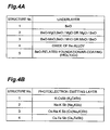
- Fig. 4A is a table for explaining types of underlayer structures applied to a plurality of samples prepared as photocathodes according to the present invention
- Fig. 4B is a table for explaining types of photoelectron emitting layer structures applied to a plurality of samples prepared as photocathodes according to the present invention.
- Fig. 5 is a graph showing spectral sensitivity characteristics of photocathodes according to the present invention together with spectral sensitivity characteristics of a photocathode according to a comparative example.
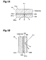
- Fig. 1A is a view showing a cross sectional structure of a transmissive photocathode as a photocathode according to the present invention.
- Fig. 1B is a view showing a cross sectional structure of a reflective photocathode as a photocathode according to the present invention.
- the transmissive photocathode 1A shown in Fig. 1A comprises a supporting substrate 100A that transmits an incident light hv with a predetermined wavelength, an underlayer 200 provided on the supporting substrate 100A, and a photoelectron emitting layer 300 provided on the underlayer 200.
- the supporting substrate 100A has a first main surface 101a that functions as a light incident surface of the transmissive photocathode 1A, and a second main surface 102a opposing the first main surface 101a.
- the photoelectron emitting layer 300 has a first main surface 301a that opposes the second main surface 102a of the supporting substrate 100A and a second main surface 302a that opposes the first main surface 301a, and then functions as a photoelectron emitting surface of the transmissive photocathode 1A.
- the underlayer 200 is arranged between the supporting substrate 100A and the photoelectron emitting layer 300 while being in direct contact with both the second main surface 102a of the supporting substrate 100A and the first main surface 301 a of the photoelectron emitting layer 300.
- an incident light hv is made incident from the supporting substrate 100A side and electrons e - are emitted from the photoelectron emitting layer 300 side in response to the incident light hv.
- a reflective photocathode 1B shown in Fig. 1B comprises a supporting substrate 100B that blocks an incident light hv with a predetermined wavelength, an underlayer 200 provided on the supporting substrate 100B, and a photoelectron emitting layer provided on the underlayer 200.
- the supporting substrate 100B has a first main surface 101b and a second main surface 102b opposing the first main surface 101b.
- the photoelectron emitting layer 300 has a first main surface 301b opposing the second main surface 102b of the supporting substrate 100B and a second main surface 302b opposing the first main surface 301b, and functions as both a light incident surface and a photoelectron emitting surface of the reflective photocathode 1B.
- the underlayer 200 is arranged between the supporting substrate 100B and the photoelectron emitting layer 300 while being in direct contact with both the second main surface 102b of the supporting substrate 100B and the first main surface 301b of the photoelectron emitting layer 300. That is, for this reflective photocathode 1B, when an incident light hv has reached the supporting substrate 100B from the photoelectron emitting layer 300, photoelectrons e - are emitted from the supporting substrate 100B in a direction toward the photoelectron emitting layer 300 in response to the incident light hv.
- the supporting substrate 100B is comprised of a metal material such as a nickel supporting substrate since this functions as a reinforcing member to support the photoelectron emitting layer 300.
- the underlayer 200 and the photoelectron emitting layer 300 may have the same structures.
- the underlayer 200 contains a Be element.
- the underlayer 200 can be realized by various structures, such as a single-layer structure comprised of an oxide of a Be-alloy or BeO, and a multi-layer structure including a layer (BeO-related foundation) containing, as a main material, BeO or a BeO single-layer.
- the photoelectron emitting layer 300 is comprised of a compound of antimony (Sb) and an alkali metal.
- the alkali metal contains at least one of cesium (Cs), potassium (K), and sodium (Na).
- Cs cesium
- K potassium
- Na sodium
- Fig. 2 is a view showing a cross sectional structure of a photomultiplier (included in an electron tube according to the present invention) applied with the aforementioned transmissive photocathode 1A.
- the transmissive photoelectron tube 10A comprises a transparent container 32 having a faceplate that transmits an incident light hv.
- the faceplate of the transparent container 32 functions as the supporting substrate 100A of the transmissive photocathode 1A.
- a photoelectron emitting layer 300 via an underlayer 200, and provided is a focusing electrode 36 that guides emitted photoelectrons to an electron multiplier section 40, the electron multiplier section 40 that has a plurality of stages of dynodes for cascade-multiplying secondary electrons, and an anode 38 that collects multiplied secondary electrons.
- the transparent container 32 accommodates at least, a part of the transmissive photocathode 1A, the electron multiplier section 40 and the anode 38.
- the electron multiplier section 40 provided between the focusing electrode 36 and anode 38 is constituted by a plurality of dynodes (electrodes) 42. Each dynode 42 is electrically connected with a stem pin 44 provided so as to penetrate through the container 32.
- FIG. 3 is a view showing a coross sectional structure of a photomultiplier (included in an electron tube according to the present invention) applied with the aforementioned reflective photocathode 1B.
- the reflective photoelectron tube 10B comprises a transparent container 32 having a faceplate that transmits an incident light hv
- the whole of the reflective photocathode 1B including the supporting substrate 100B is arranged in the transparent container 32.
- an electron multiplier section 40 that has a plurality of stages of dynodes for cascade-multiplying photoelectrons emitted from the reflective photocathode 1B, and an anode 38 that collects secondary electrons multiplied by the electron multiplier section 40.
- the transparent container 32 accommodates at least, the whole of the reflective photocathode 1B, the electron multiplier section 40, and the anode 38.
- the electron multiplier section 40 provided between the reflective photocathode 1B and anode 38 is constituted by a plurality of dynodes (electrodes) 42. Each dynode 42 is electrically connected with a stem pin provided so as to penetrate through the transparent container 32.
- Fig. 4A is a table for explaining types of underlayer structures applied to a plurality of samples (hereinafter, referred to as transmissive samples) prepared as the photocathode 1A.
- Fig. 4B is a table for explaining types of photoelectron emitting layer structures applied to a plurality of prepared transmissive samples. That is, the types of prepared transmissive samples are 20 types obtained by combination of five types of underlayers 200 and four types of photoelectron emitting layers 300.
- structure No. 1 of the underlayer 200 is a BeO single layer.
- Structure No. 2 of the underlayer 200 is a double-layer structure of an MgO single layer and a BeO single layer.
- an alloy BeO-MgO
- either single layer may contact with the supporting substrate 100.
- BeO may be formed after formation of MgO, and MgO and BeO may be simultaneously vapor-deposited.
- 3 of the underlayer 200 is a double-layer structure of a MnO single layer and a BeO single layer, and at an interface between the MnO single layer and BeO single layer, an alloy (BeO-MnO) is formed.
- either single layer may contact with the supporting substrate 100.
- BeO may be formed after formation of MnO, and MnO and BeO may be simultaneously vapor-deposited.
- Structure No. 4 of the underlayer 200 is a single layer comprised of an oxide of a Be-alloy. As structure No.
- a thin film of HfO 2 and Y 2 O 3 is provided on the supporting substrate 100, and provided on the thin film is a BeO-related foundation (which can be one of the above-mentioned structures No. 1 to No. 4).
- the thin film can function as an anti-reflection (AR) coating against an incident light.
- AR anti-reflection
- the film thickness of HfO 2 or Y 2 O 3 is selected from a range of 30 ⁇ to 2000 ⁇ .
- structure No. 1 of the photoelectron emitting layer 300 is a K-CsSb (K 2 CsSb) single layer.
- Structure No. 2 of the photoelectron emitting layer 300 is a Na-KSb (Na 2 KSb) single layer.
- Structure No. 3 of the photoelectron emitting layer 300 is a Cs-Na-KSb (Cs(Na 2 K)Sb) single layer.
- Structure No. 4 of the photoelectron emitting layer 300 is a Cs-TeSb (Cs 2 TeSb) single layer.
- the aforementioned MnO x , MeO, and the like are known as materials that transmit light with a wavelength of 300nm to 1000nm.
- the thin-film material HfO 2 exhibits a high transmittance to a light with a wavelength of 300nm to 1000nm.
- Fig. 5 is a graph showing sensitivity characteristics of transmissive samples with the structures as described above prepared as photocathodes according to the present invention. together with sensitivity characteristics of a comparative sample of a transmissive photocathode according to a comparative example.
- a graph G510 in Fig. 5 shows spectral sensitivity characteristics of a first transmissive sample having a combination of the aforementioned underlayer structure No. 2 (mixed crystals of BeO and MgO (a mass ratio of Be and Mg is 9:1)) and photoelectron emitting layer structure No.
- a graph G520 shows spectral sensitivity characteristics of a comparative sample, which is a photocathode according to a comparative example
- a graph G530 shows spectral sensitivity characteristics of a second transmissive sample having a combination of the aforementioned underlayer structure No. 5 (mixed crystals of BeO and MgO with a mass ratio of Be and Mg set to 9:1 are formed on an HfO 2 coating) and photoelectron emitting layer structure No. 1.
- the supporting substrate 100A is composed of borosilicate glass
- the underlayer 200 is composed of mixed crystals of BeO and MgO (MgO and BeO are simultaneously vapor-deposited on the supporting substrate 100A) with a mass ratio of Be and Mg set to 9:1
- the photoelectron emitting layer 300 is composed of a K-CsSb layer.
- the thickness of the underlayer 200 is 100 ⁇
- the thickness of the photoelectron emitting layer 300 is 160 ⁇
- a ratio of the thickness of the photoelectron emitting layer 300 to the thickness of the underlayer 200 is 1.6.
- the supporting substrate is composed of borosilicate glass
- the underlayer is composed of an MnO X single layer
- the photoelectron emitting layer is composed of a K-CsSb layer.
- the thickness of the underlayer is 30 ⁇
- the thickness of the photoelectron emitting layer is 160 ⁇
- a ratio of the thickness of the photoelectron emitting layer to the thickness of the underlayer is 5.3.
- the supporting substrate 100A is composed of borosilicate glass.
- the underlayer 200 is composed of HfO 2 vapor-deposited as an AR coating on the supporting substrate 100A and mixed crystals of BeO and MgO (MgO and BeO are simultaneously vapor-deposited on the HfO 2 coating) with a mass ratio of Be and Mg set to 9:1.
- the photoelectron emitting layer 300 is composed of a K-CsSb layer.
- the thickness of the underlayer 200 is 400 ⁇ (the thickness of the HfO 2 is 300 ⁇ ; the thickness of the mixed cristals of BeO and MgO is 100 ⁇ ), the thickness of the photoelectron emitting layer 300 is 160 ⁇ , and a ratio of the thickness of the photoelectron emitting layer 300 to the thickness of the underlayer 200 is 0.4.
- a ratio of the thickness of the photoelectron emitting layer 300 to the thickness of the layer constituted by the mixed crystals of BeO and MgO is 1.6.
- the transmissive samples prepared as photocathodes according to the present invention has been improved in quantum efficiency in the entire usable wavelength range in comparison with the comparative sample.
- the quantum efficiency at a wavelength of 360nm is 26.9% in the comparative sample, while in the first transmissive sample, this is 40.8%, and in the second transmissive sample, 44.8%, so that an increase in sensitivity of about 50% or more has been confirmed.
- the thickness of the underlayer 200 is set such that the ratio of the thickness of the photoelectron emitting layer 300 to the thickness of the underlayer 200 is within a range of 0.1 or more but 100 or less. In addition, it is preferable that the thickness of the underlayer 200 is set so as to be within a range of 20 ⁇ to 500 ⁇ , and the thickness of the photoelectron emitting layer 300, within a range of 50 ⁇ and 2000 ⁇ .
- the quantum efficiency of the various transmissive samples at the wavelength 360 nm, obtained by changing the structure of the underlayer 200 to the K-CsSb photoelectron emitting layer 300 become as follows. That is, in the case of the underlayer 200 provided as a BeO single layer (structure No. 1), the quantum efficiency of the obtained transmissive sample was 38.8%. In addition, in the case of the underlayer 200 with structure No. 2 where BeO was vapor-deposited after vapor deposition of MgO, the quantum efficiency of the obtained transmissive sample was 38%. Further, in the case of the underlayer 200 composed of mixed crystals of BeO and MnO (the mass ratio of Be and Mn was 9:1) (structure 3), the quantum efficiency of the obtained transmissive sample was 38%.
- the quantum efficiency of the obtained transmissive sample was 41.2%. Further, in the case of the underlayer 200 composed of mixed crystals of BeO and HfO 2 (the mass ratio of Be and Hf was 9:1) (structure 3), the quantum efficiency of the obtained transmissive sample was 39.6%. In the transmissive samples having any underlayer structures, an increase in sensitivity in comparison with the comparative sample was confirmed.
- the second transmissive sample including the supporting substrate 100A of borosilicate glass, the underlayer 200 composed of a HfO 2 coating and mixed crystals of BeO and MgO, and the K-CsSb photoelectron emitting layer 300
- a high quantum efficiency with a peak of 44.8% could be obtained as shown in Fig. 5 .
- the fact that the samples prepared as photocathodes according to the present invention were markedly improved in spectral sensitivity in comparison with the comparative sample as described above is considered to be due to that the underlayer 200 containing BeO functions as a barrier layer.
- an alkali metal for example, K, Cs, and the like
- an alkali metal contained in the photoelectron emitting layer 300 is dispersed at the time of heat treatment in a manufacturing process of the photocathode and thus considered to move to a layer adjacent to the photoelectron emitting layer 300. In this case, it is assumed that a decline in the effective quantum efficiency results therefrom.
- the underlayer 200 containing BeO when the underlayer 200 containing BeO is provided as an adjacent layer in contact with the photoelectron emitting layer 300, it is considered that diffusion of an alkali metal (for example, K, Cs, and the like) contained in the photoelectron emitting layer 300 is effectively suppressed at the time of heat treatment in a manufacturing process.
- an alkali metal for example, K, Cs, and the like
- this underlayer 200 functions so as to reverse the direction of, out of photoelectrons generated within the photoelectron emitting layer 300, photoelectrons traveling toward the supporting substrate 100 side. For this reason, it is considered that the quantum efficiency of the photocathode as a whole is dramatically improved.
- the photocathode according to the present invention is dramatically improved in the effective quantum efficiency in comparison with the conventional photocathode.
Landscapes
- Common Detailed Techniques For Electron Tubes Or Discharge Tubes (AREA)
Applications Claiming Priority (1)
| Application Number | Priority Date | Filing Date | Title |
|---|---|---|---|
| US87737006P | 2006-12-28 | 2006-12-28 |
Publications (3)
| Publication Number | Publication Date |
|---|---|
| EP1939917A2 true EP1939917A2 (fr) | 2008-07-02 |
| EP1939917A3 EP1939917A3 (fr) | 2008-07-23 |
| EP1939917B1 EP1939917B1 (fr) | 2015-02-25 |
Family
ID=39284277
Family Applications (1)
| Application Number | Title | Priority Date | Filing Date |
|---|---|---|---|
| EP07024966.9A Active EP1939917B1 (fr) | 2006-12-28 | 2007-12-21 | Photocathode, tube photomultiplicateur et tube d'électron |
Country Status (4)
| Country | Link |
|---|---|
| US (1) | US8421354B2 (fr) |
| EP (1) | EP1939917B1 (fr) |
| JP (1) | JP5342769B2 (fr) |
| CN (1) | CN101211730B (fr) |
Cited By (27)
| Publication number | Priority date | Publication date | Assignee | Title |
|---|---|---|---|---|
| US8212475B2 (en) | 2009-04-02 | 2012-07-03 | Hamamatsu Photonics K.K. | Photocathode, electron tube, and photomultiplier tube |
| US9347890B2 (en) | 2013-12-19 | 2016-05-24 | Kla-Tencor Corporation | Low-noise sensor and an inspection system using a low-noise sensor |
| US9410901B2 (en) | 2014-03-17 | 2016-08-09 | Kla-Tencor Corporation | Image sensor, an inspection system and a method of inspecting an article |
| US9419407B2 (en) | 2014-09-25 | 2016-08-16 | Kla-Tencor Corporation | Laser assembly and inspection system using monolithic bandwidth narrowing apparatus |
| US9426400B2 (en) | 2012-12-10 | 2016-08-23 | Kla-Tencor Corporation | Method and apparatus for high speed acquisition of moving images using pulsed illumination |
| US9478402B2 (en) | 2013-04-01 | 2016-10-25 | Kla-Tencor Corporation | Photomultiplier tube, image sensor, and an inspection system using a PMT or image sensor |
| US9496425B2 (en) | 2012-04-10 | 2016-11-15 | Kla-Tencor Corporation | Back-illuminated sensor with boron layer |
| US9529182B2 (en) | 2013-02-13 | 2016-12-27 | KLA—Tencor Corporation | 193nm laser and inspection system |
| US9601299B2 (en) | 2012-08-03 | 2017-03-21 | Kla-Tencor Corporation | Photocathode including silicon substrate with boron layer |
| US9608399B2 (en) | 2013-03-18 | 2017-03-28 | Kla-Tencor Corporation | 193 nm laser and an inspection system using a 193 nm laser |
| US9748294B2 (en) | 2014-01-10 | 2017-08-29 | Hamamatsu Photonics K.K. | Anti-reflection layer for back-illuminated sensor |
| US9748729B2 (en) | 2014-10-03 | 2017-08-29 | Kla-Tencor Corporation | 183NM laser and inspection system |
| US9768577B2 (en) | 2012-12-05 | 2017-09-19 | Kla-Tencor Corporation | Semiconductor inspection and metrology system using laser pulse multiplier |
| US9767986B2 (en) | 2014-08-29 | 2017-09-19 | Kla-Tencor Corporation | Scanning electron microscope and methods of inspecting and reviewing samples |
| US9804101B2 (en) | 2014-03-20 | 2017-10-31 | Kla-Tencor Corporation | System and method for reducing the bandwidth of a laser and an inspection system and method using a laser |
| US9860466B2 (en) | 2015-05-14 | 2018-01-02 | Kla-Tencor Corporation | Sensor with electrically controllable aperture for inspection and metrology systems |
| US10175555B2 (en) | 2017-01-03 | 2019-01-08 | KLA—Tencor Corporation | 183 nm CW laser and inspection system |
| US10197501B2 (en) | 2011-12-12 | 2019-02-05 | Kla-Tencor Corporation | Electron-bombarded charge-coupled device and inspection systems using EBCCD detectors |
| US10313622B2 (en) | 2016-04-06 | 2019-06-04 | Kla-Tencor Corporation | Dual-column-parallel CCD sensor and inspection systems using a sensor |
| US10462391B2 (en) | 2015-08-14 | 2019-10-29 | Kla-Tencor Corporation | Dark-field inspection using a low-noise sensor |
| US10748730B2 (en) | 2015-05-21 | 2020-08-18 | Kla-Tencor Corporation | Photocathode including field emitter array on a silicon substrate with boron layer |
| US10778925B2 (en) | 2016-04-06 | 2020-09-15 | Kla-Tencor Corporation | Multiple column per channel CCD sensor architecture for inspection and metrology |
| WO2020243795A1 (fr) * | 2019-06-07 | 2020-12-10 | Adaptas Solutions Pty Ltd | Détecteur comprenant un moyen d'émission d'électrons secondaires de transmission |
| US10943760B2 (en) | 2018-10-12 | 2021-03-09 | Kla Corporation | Electron gun and electron microscope |
| US11114489B2 (en) | 2018-06-18 | 2021-09-07 | Kla-Tencor Corporation | Back-illuminated sensor and a method of manufacturing a sensor |
| US11114491B2 (en) | 2018-12-12 | 2021-09-07 | Kla Corporation | Back-illuminated sensor and a method of manufacturing a sensor |
| US11848350B2 (en) | 2020-04-08 | 2023-12-19 | Kla Corporation | Back-illuminated sensor and a method of manufacturing a sensor using a silicon on insulator wafer |
Families Citing this family (12)
| Publication number | Priority date | Publication date | Assignee | Title |
|---|---|---|---|---|
| US8873596B2 (en) | 2011-07-22 | 2014-10-28 | Kla-Tencor Corporation | Laser with high quality, stable output beam, and long life high conversion efficiency non-linear crystal |
| WO2013036576A1 (fr) | 2011-09-07 | 2013-03-14 | Kla-Tencor Corporation | Photocathode transmissive-réfléchissante |
| CN103715033A (zh) * | 2013-12-27 | 2014-04-09 | 中国科学院西安光学精密机械研究所 | 一种高灵敏度锑碱光电阴极和光电倍增管 |
| US10453660B2 (en) | 2016-01-29 | 2019-10-22 | Shenzhen Genorivision Technology Co., Ltd. | Photomultiplier and methods of making it |
| JP6974210B2 (ja) * | 2018-02-22 | 2021-12-01 | 浜松ホトニクス株式会社 | イオン検出器 |
| CN108281337B (zh) * | 2018-03-23 | 2024-04-05 | 中国工程物理研究院激光聚变研究中心 | 光电阴极及x射线诊断系统 |
| JP7330268B2 (ja) * | 2018-10-05 | 2023-08-21 | アダプタス ソリューションズ プロプライエタリー リミテッド | 電子増倍管の内部領域の改善 |
| CN111223739B (zh) * | 2018-11-26 | 2023-11-24 | 陈新云 | 新型铜铍合金倍增级及其制备方法 |
| WO2020261704A1 (fr) | 2019-06-26 | 2020-12-30 | 浜松ホトニクス株式会社 | Photocathode, tube électronique et procédé de production de photocathode |
| CN112908807B (zh) * | 2021-01-13 | 2024-07-02 | 陕西理工大学 | 一种光电阴极及其应用 |
| CN113512470A (zh) * | 2021-03-31 | 2021-10-19 | 杭州安誉科技有限公司 | 光电倍增管用光电阴极及其制备方法 |
| US12387924B2 (en) | 2023-07-24 | 2025-08-12 | Hamamatsu Photonics K.K. | Photomultiplier tube including a protective layer |
Family Cites Families (29)
| Publication number | Priority date | Publication date | Assignee | Title |
|---|---|---|---|---|
| GB1005708A (en) | 1960-12-14 | 1965-09-29 | Emi Ltd | Improvements relating to photo electrically sensitive devices |
| US3631303A (en) | 1970-01-19 | 1971-12-28 | Varian Associates | Iii-v cathodes having a built-in gradient of potential energy for increasing the emission efficiency |
| JPS5247665B2 (fr) | 1972-02-14 | 1977-12-03 | ||
| JPS529499B2 (fr) | 1972-12-18 | 1977-03-16 | ||
| US4339469A (en) * | 1979-11-29 | 1982-07-13 | Rca Corporation | Method of making potassium, cesium, rubidium, antimony photocathode |
| US4311939A (en) * | 1980-03-21 | 1982-01-19 | Rca Corporation | Alkali antimonide layer on a beryllim-copper primary dynode |
| US4341427A (en) * | 1980-06-30 | 1982-07-27 | Rca Corporation | Method for stabilizing the anode sensitivity of a photomultiplier tube |
| FR2493036A1 (fr) | 1980-07-30 | 1982-04-30 | Hyperelec | Photocathode bialcaline a reponse spectrale elargie et procede de fabrication |
| FR2498321A1 (fr) | 1981-01-21 | 1982-07-23 | Labo Electronique Physique | Structure de detection photoelectrique |
| US4639638A (en) * | 1985-01-28 | 1987-01-27 | Sangamo Weston, Inc. | Photomultiplier dynode coating materials and process |
| JPS6220654A (ja) | 1985-07-19 | 1987-01-29 | Toyota Motor Corp | 車両用エンジン制御装置の電源回路 |
| US5304815A (en) * | 1986-09-11 | 1994-04-19 | Canon Kabushiki Kaisha | Electron emission elements |
| DE3752064T2 (de) | 1986-09-11 | 1997-11-06 | Canon Kk | Elektronenemittierendes Element |
| DE8710514U1 (de) | 1987-07-31 | 1987-09-24 | Fag Kugelfischer Georg Schaefer Kgaa, 8720 Schweinfurt | Käfig für ein Segmentwälzlager |
| JPH0552444A (ja) | 1991-08-20 | 1993-03-02 | Sanyo Electric Co Ltd | エンジン駆動ヒートポンプ装置 |
| JP2500209B2 (ja) | 1991-09-11 | 1996-05-29 | 浜松ホトニクス株式会社 | 反射型光電面および光電子増倍管 |
| JP2758529B2 (ja) | 1992-04-22 | 1998-05-28 | 浜松ホトニクス株式会社 | 反射型光電面および光電子増倍管 |
| JP2923395B2 (ja) | 1992-08-24 | 1999-07-26 | 浜松ホトニクス株式会社 | 光電面および光電子増倍管 |
| JPH0883561A (ja) | 1994-09-13 | 1996-03-26 | Hamamatsu Photonics Kk | 二次電子増倍電極および光電子増倍管 |
| JPH0896705A (ja) * | 1994-09-27 | 1996-04-12 | Hamamatsu Photonics Kk | 半導体光電陰極及び光電管 |
| JP3524249B2 (ja) * | 1996-01-16 | 2004-05-10 | 浜松ホトニクス株式会社 | 電子管 |
| JPH11135003A (ja) * | 1997-10-28 | 1999-05-21 | Hamamatsu Photonics Kk | 光電面及びそれを用いた電子管 |
| JP3429671B2 (ja) * | 1998-04-13 | 2003-07-22 | 浜松ホトニクス株式会社 | 光電陰極及び電子管 |
| JP4984362B2 (ja) | 2001-06-12 | 2012-07-25 | 東ソー株式会社 | ハイドロタルサイト類化合物結晶の製造方法 |
| JP4116294B2 (ja) | 2002-01-07 | 2008-07-09 | 浜松ホトニクス株式会社 | 光電面および光電変換管 |
| EP1521286A4 (fr) * | 2003-01-17 | 2006-12-13 | Hamamatsu Photonics Kk | Agent de generation de metal alcalin, generateur de metal alcalin, surface photoelectrique, surface d'emission electronique secondaire, tube electronique, methode de fabrication d'une surface photoelectrique, methode de fabrication d'une surface d'emission electronique secondaire et methode de fabri |
| EP1585159A4 (fr) * | 2003-01-17 | 2006-12-13 | Hamamatsu Photonics Kk | Agent de generation de metal alcalin, generateur de metal alcalin, surface photoelectrique, surface d'emission electronique secondaire, tube electronique, methode de fabrication d'une surface photoelectrique, methode de fabrication d'une surface d'emission electronique secondaire et methode de fabri |
| EP1730795A2 (fr) * | 2004-03-31 | 2006-12-13 | Matsushita Electric Industrial Co., Ltd. | Élément de conversion photoélectrique organique et sa méthode de production, photodiode organique et capteur d"images l"utilisant, diode organique et sa méthode de production |
| JP4885072B2 (ja) | 2006-07-27 | 2012-02-29 | 株式会社リコー | 位置検出装置、および画像形成装置 |
-
2007
- 2007-11-26 JP JP2007305060A patent/JP5342769B2/ja active Active
- 2007-12-19 US US11/960,169 patent/US8421354B2/en active Active
- 2007-12-21 EP EP07024966.9A patent/EP1939917B1/fr active Active
- 2007-12-28 CN CN2007103058945A patent/CN101211730B/zh active Active
Non-Patent Citations (1)
| Title |
|---|
| None |
Cited By (44)
| Publication number | Priority date | Publication date | Assignee | Title |
|---|---|---|---|---|
| US8212475B2 (en) | 2009-04-02 | 2012-07-03 | Hamamatsu Photonics K.K. | Photocathode, electron tube, and photomultiplier tube |
| US10197501B2 (en) | 2011-12-12 | 2019-02-05 | Kla-Tencor Corporation | Electron-bombarded charge-coupled device and inspection systems using EBCCD detectors |
| US9496425B2 (en) | 2012-04-10 | 2016-11-15 | Kla-Tencor Corporation | Back-illuminated sensor with boron layer |
| US10121914B2 (en) | 2012-04-10 | 2018-11-06 | Kla-Tencor Corporation | Back-illuminated sensor with boron layer |
| US10446696B2 (en) | 2012-04-10 | 2019-10-15 | Kla-Tencor Corporation | Back-illuminated sensor with boron layer |
| US9818887B2 (en) | 2012-04-10 | 2017-11-14 | Kla-Tencor Corporation | Back-illuminated sensor with boron layer |
| US11081310B2 (en) | 2012-08-03 | 2021-08-03 | Kla-Tencor Corporation | Photocathode including silicon substrate with boron layer |
| US9601299B2 (en) | 2012-08-03 | 2017-03-21 | Kla-Tencor Corporation | Photocathode including silicon substrate with boron layer |
| US10199197B2 (en) | 2012-08-03 | 2019-02-05 | Kla-Tencor Corporation | Photocathode including silicon substrate with boron layer |
| US9768577B2 (en) | 2012-12-05 | 2017-09-19 | Kla-Tencor Corporation | Semiconductor inspection and metrology system using laser pulse multiplier |
| US9426400B2 (en) | 2012-12-10 | 2016-08-23 | Kla-Tencor Corporation | Method and apparatus for high speed acquisition of moving images using pulsed illumination |
| US9529182B2 (en) | 2013-02-13 | 2016-12-27 | KLA—Tencor Corporation | 193nm laser and inspection system |
| US9935421B2 (en) | 2013-02-13 | 2018-04-03 | Kla-Tencor Corporation | 193nm laser and inspection system |
| US10439355B2 (en) | 2013-02-13 | 2019-10-08 | Kla-Tencor Corporation | 193nm laser and inspection system |
| US9608399B2 (en) | 2013-03-18 | 2017-03-28 | Kla-Tencor Corporation | 193 nm laser and an inspection system using a 193 nm laser |
| US9478402B2 (en) | 2013-04-01 | 2016-10-25 | Kla-Tencor Corporation | Photomultiplier tube, image sensor, and an inspection system using a PMT or image sensor |
| US9620341B2 (en) | 2013-04-01 | 2017-04-11 | Kla-Tencor Corporation | Photomultiplier tube, image sensor, and an inspection system using a PMT or image sensor |
| US9347890B2 (en) | 2013-12-19 | 2016-05-24 | Kla-Tencor Corporation | Low-noise sensor and an inspection system using a low-noise sensor |
| US9748294B2 (en) | 2014-01-10 | 2017-08-29 | Hamamatsu Photonics K.K. | Anti-reflection layer for back-illuminated sensor |
| US10269842B2 (en) | 2014-01-10 | 2019-04-23 | Hamamatsu Photonics K.K. | Anti-reflection layer for back-illuminated sensor |
| US9620547B2 (en) | 2014-03-17 | 2017-04-11 | Kla-Tencor Corporation | Image sensor, an inspection system and a method of inspecting an article |
| US9410901B2 (en) | 2014-03-17 | 2016-08-09 | Kla-Tencor Corporation | Image sensor, an inspection system and a method of inspecting an article |
| US10495582B2 (en) | 2014-03-20 | 2019-12-03 | Kla-Tencor Corporation | System and method for reducing the bandwidth of a laser and an inspection system and method using a laser |
| US9804101B2 (en) | 2014-03-20 | 2017-10-31 | Kla-Tencor Corporation | System and method for reducing the bandwidth of a laser and an inspection system and method using a laser |
| US10466212B2 (en) | 2014-08-29 | 2019-11-05 | KLA—Tencor Corporation | Scanning electron microscope and methods of inspecting and reviewing samples |
| US9767986B2 (en) | 2014-08-29 | 2017-09-19 | Kla-Tencor Corporation | Scanning electron microscope and methods of inspecting and reviewing samples |
| US9419407B2 (en) | 2014-09-25 | 2016-08-16 | Kla-Tencor Corporation | Laser assembly and inspection system using monolithic bandwidth narrowing apparatus |
| US10199149B2 (en) | 2014-10-03 | 2019-02-05 | Kla-Tencor Corporation | 183NM laser and inspection system |
| US9748729B2 (en) | 2014-10-03 | 2017-08-29 | Kla-Tencor Corporation | 183NM laser and inspection system |
| US9860466B2 (en) | 2015-05-14 | 2018-01-02 | Kla-Tencor Corporation | Sensor with electrically controllable aperture for inspection and metrology systems |
| US10194108B2 (en) | 2015-05-14 | 2019-01-29 | Kla-Tencor Corporation | Sensor with electrically controllable aperture for inspection and metrology systems |
| US10748730B2 (en) | 2015-05-21 | 2020-08-18 | Kla-Tencor Corporation | Photocathode including field emitter array on a silicon substrate with boron layer |
| US10462391B2 (en) | 2015-08-14 | 2019-10-29 | Kla-Tencor Corporation | Dark-field inspection using a low-noise sensor |
| US10313622B2 (en) | 2016-04-06 | 2019-06-04 | Kla-Tencor Corporation | Dual-column-parallel CCD sensor and inspection systems using a sensor |
| US10778925B2 (en) | 2016-04-06 | 2020-09-15 | Kla-Tencor Corporation | Multiple column per channel CCD sensor architecture for inspection and metrology |
| US10764527B2 (en) | 2016-04-06 | 2020-09-01 | Kla-Tencor Corporation | Dual-column-parallel CCD sensor and inspection systems using a sensor |
| US10429719B2 (en) | 2017-01-03 | 2019-10-01 | Kla-Tencor Corporation | 183 nm CW laser and inspection system |
| US10175555B2 (en) | 2017-01-03 | 2019-01-08 | KLA—Tencor Corporation | 183 nm CW laser and inspection system |
| US11114489B2 (en) | 2018-06-18 | 2021-09-07 | Kla-Tencor Corporation | Back-illuminated sensor and a method of manufacturing a sensor |
| US10943760B2 (en) | 2018-10-12 | 2021-03-09 | Kla Corporation | Electron gun and electron microscope |
| US11114491B2 (en) | 2018-12-12 | 2021-09-07 | Kla Corporation | Back-illuminated sensor and a method of manufacturing a sensor |
| WO2020243795A1 (fr) * | 2019-06-07 | 2020-12-10 | Adaptas Solutions Pty Ltd | Détecteur comprenant un moyen d'émission d'électrons secondaires de transmission |
| US11869757B2 (en) | 2019-06-07 | 2024-01-09 | Adaptas Solutions Pty Ltd | Detector comprising transmission secondary electron emission means |
| US11848350B2 (en) | 2020-04-08 | 2023-12-19 | Kla Corporation | Back-illuminated sensor and a method of manufacturing a sensor using a silicon on insulator wafer |
Also Published As
| Publication number | Publication date |
|---|---|
| US20100096985A1 (en) | 2010-04-22 |
| CN101211730B (zh) | 2011-11-09 |
| JP5342769B2 (ja) | 2013-11-13 |
| EP1939917A3 (fr) | 2008-07-23 |
| US8421354B2 (en) | 2013-04-16 |
| EP1939917B1 (fr) | 2015-02-25 |
| JP2008166262A (ja) | 2008-07-17 |
| CN101211730A (zh) | 2008-07-02 |
Similar Documents
| Publication | Publication Date | Title |
|---|---|---|
| EP1939917B1 (fr) | Photocathode, tube photomultiplicateur et tube d'électron | |
| JP5563869B2 (ja) | 光電陰極、電子管及び光電子増倍管 | |
| CN101379582B (zh) | 光电面、具备该光电面的电子管以及光电面的制造方法 | |
| EP0532358B1 (fr) | Photo-cathode du type à réflection et photomultiplicateur l'utilisant | |
| EP2309529B1 (fr) | Photocathode | |
| WO2016104243A1 (fr) | Surface photoélectrique, tube de conversion photoélectrique, intensificateur d'image et tube photomultiplicateur | |
| JP6720427B1 (ja) | 光電陰極、電子管、及び、光電陰極の製造方法 | |
| EP1513185A1 (fr) | Surface photoelectrique a semi-conducteur et procede de fabrication correspondant, et tube photodetecteur utilisant cette surface photoelectrique a semiconducteur | |
| US5557166A (en) | Reflection-type photoelectronic surface and photomultiplier | |
| JP2651329B2 (ja) | 光電子または2次電子放射用陰極 | |
| RU2780041C1 (ru) | Микроканальная пластина | |
| JP7733280B1 (ja) | 光電陰極及び電子管 | |
| WO2026033960A1 (fr) | Photocathode et tube électronique | |
| JP2025017306A (ja) | 光電子増倍管 | |
| JPH10172503A (ja) | 光電子増倍管 | |
| CN119361411A (zh) | 光电倍增管 | |
| JP4975400B2 (ja) | 撮像管 | |
| JP2009217996A (ja) | 光電陰極、電子管及びイメージインテンシファイア |
Legal Events
| Date | Code | Title | Description |
|---|---|---|---|
| PUAI | Public reference made under article 153(3) epc to a published international application that has entered the european phase |
Free format text: ORIGINAL CODE: 0009012 |
|
| PUAL | Search report despatched |
Free format text: ORIGINAL CODE: 0009013 |
|
| AK | Designated contracting states |
Kind code of ref document: A2 Designated state(s): AT BE BG CH CY CZ DE DK EE ES FI FR GB GR HU IE IS IT LI LT LU LV MC MT NL PL PT RO SE SI SK TR |
|
| AX | Request for extension of the european patent |
Extension state: AL BA HR MK RS |
|
| AK | Designated contracting states |
Kind code of ref document: A3 Designated state(s): AT BE BG CH CY CZ DE DK EE ES FI FR GB GR HU IE IS IT LI LT LU LV MC MT NL PL PT RO SE SI SK TR |
|
| AX | Request for extension of the european patent |
Extension state: AL BA HR MK RS |
|
| 17P | Request for examination filed |
Effective date: 20090121 |
|
| AKX | Designation fees paid |
Designated state(s): DE FR GB |
|
| 17Q | First examination report despatched |
Effective date: 20120730 |
|
| GRAP | Despatch of communication of intention to grant a patent |
Free format text: ORIGINAL CODE: EPIDOSNIGR1 |
|
| RIC1 | Information provided on ipc code assigned before grant |
Ipc: H01J 1/34 20060101AFI20140814BHEP Ipc: H01J 1/35 20060101ALI20140814BHEP Ipc: H01J 43/00 20060101ALI20140814BHEP |
|
| INTG | Intention to grant announced |
Effective date: 20140908 |
|
| GRAS | Grant fee paid |
Free format text: ORIGINAL CODE: EPIDOSNIGR3 |
|
| GRAA | (expected) grant |
Free format text: ORIGINAL CODE: 0009210 |
|
| AK | Designated contracting states |
Kind code of ref document: B1 Designated state(s): DE FR GB |
|
| REG | Reference to a national code |
Ref country code: GB Ref legal event code: FG4D |
|
| RIN1 | Information on inventor provided before grant (corrected) |
Inventor name: WATASE, FUMIO Inventor name: WATANABE, HIROYUKI Inventor name: YAMASHITA, SHINICHI |
|
| REG | Reference to a national code |
Ref country code: DE Ref legal event code: R096 Ref document number: 602007040315 Country of ref document: DE Effective date: 20150409 |
|
| REG | Reference to a national code |
Ref country code: FR Ref legal event code: PLFP Year of fee payment: 9 |
|
| REG | Reference to a national code |
Ref country code: DE Ref legal event code: R097 Ref document number: 602007040315 Country of ref document: DE |
|
| PLBE | No opposition filed within time limit |
Free format text: ORIGINAL CODE: 0009261 |
|
| STAA | Information on the status of an ep patent application or granted ep patent |
Free format text: STATUS: NO OPPOSITION FILED WITHIN TIME LIMIT |
|
| 26N | No opposition filed |
Effective date: 20151126 |
|
| REG | Reference to a national code |
Ref country code: FR Ref legal event code: PLFP Year of fee payment: 10 |
|
| REG | Reference to a national code |
Ref country code: FR Ref legal event code: PLFP Year of fee payment: 11 |
|
| P01 | Opt-out of the competence of the unified patent court (upc) registered |
Effective date: 20230517 |
|
| PGFP | Annual fee paid to national office [announced via postgrant information from national office to epo] |
Ref country code: DE Payment date: 20251028 Year of fee payment: 19 |
|
| PGFP | Annual fee paid to national office [announced via postgrant information from national office to epo] |
Ref country code: GB Payment date: 20251030 Year of fee payment: 19 |
|
| PGFP | Annual fee paid to national office [announced via postgrant information from national office to epo] |
Ref country code: FR Payment date: 20251110 Year of fee payment: 19 |