EP1939933A2 - Transistor à couche mince, son procédé de fabrication, et dispositif d'affichage de diode électroluminescente organique l'incluant - Google Patents
Transistor à couche mince, son procédé de fabrication, et dispositif d'affichage de diode électroluminescente organique l'incluant Download PDFInfo
- Publication number
- EP1939933A2 EP1939933A2 EP07124162A EP07124162A EP1939933A2 EP 1939933 A2 EP1939933 A2 EP 1939933A2 EP 07124162 A EP07124162 A EP 07124162A EP 07124162 A EP07124162 A EP 07124162A EP 1939933 A2 EP1939933 A2 EP 1939933A2
- Authority
- EP
- European Patent Office
- Prior art keywords
- layer
- silicon layer
- amorphous silicon
- crystallization inducing
- semiconductor layer
- Prior art date
- Legal status (The legal status is an assumption and is not a legal conclusion. Google has not performed a legal analysis and makes no representation as to the accuracy of the status listed.)
- Ceased
Links
Images



Classifications
-
- H—ELECTRICITY
- H10—SEMICONDUCTOR DEVICES; ELECTRIC SOLID-STATE DEVICES NOT OTHERWISE PROVIDED FOR
- H10D—INORGANIC ELECTRIC SEMICONDUCTOR DEVICES
- H10D30/00—Field-effect transistors [FET]
- H10D30/60—Insulated-gate field-effect transistors [IGFET]
- H10D30/67—Thin-film transistors [TFT]
- H10D30/6729—Thin-film transistors [TFT] characterised by the electrodes
- H10D30/673—Thin-film transistors [TFT] characterised by the electrodes characterised by the shapes, relative sizes or dispositions of the gate electrodes
- H10D30/6731—Top-gate only TFTs
-
- H—ELECTRICITY
- H10—SEMICONDUCTOR DEVICES; ELECTRIC SOLID-STATE DEVICES NOT OTHERWISE PROVIDED FOR
- H10P—GENERIC PROCESSES OR APPARATUS FOR THE MANUFACTURE OR TREATMENT OF DEVICES COVERED BY CLASS H10
- H10P14/00—Formation of materials, e.g. in the shape of layers or pillars
- H10P14/20—Formation of materials, e.g. in the shape of layers or pillars of semiconductor materials
- H10P14/34—Deposited materials, e.g. layers
- H10P14/3402—Deposited materials, e.g. layers characterised by the chemical composition
- H10P14/3404—Deposited materials, e.g. layers characterised by the chemical composition being Group IVA materials
- H10P14/3411—Silicon, silicon germanium or germanium
-
- H—ELECTRICITY
- H10—SEMICONDUCTOR DEVICES; ELECTRIC SOLID-STATE DEVICES NOT OTHERWISE PROVIDED FOR
- H10D—INORGANIC ELECTRIC SEMICONDUCTOR DEVICES
- H10D86/00—Integrated devices formed in or on insulating or conducting substrates, e.g. formed in silicon-on-insulator [SOI] substrates or on stainless steel or glass substrates
- H10D86/01—Manufacture or treatment
- H10D86/021—Manufacture or treatment of multiple TFTs
- H10D86/0221—Manufacture or treatment of multiple TFTs comprising manufacture, treatment or patterning of TFT semiconductor bodies
- H10D86/0223—Manufacture or treatment of multiple TFTs comprising manufacture, treatment or patterning of TFT semiconductor bodies comprising crystallisation of amorphous, microcrystalline or polycrystalline semiconductor materials
- H10D86/0225—Manufacture or treatment of multiple TFTs comprising manufacture, treatment or patterning of TFT semiconductor bodies comprising crystallisation of amorphous, microcrystalline or polycrystalline semiconductor materials using crystallisation-promoting species, e.g. using a Ni catalyst
-
- H—ELECTRICITY
- H10—SEMICONDUCTOR DEVICES; ELECTRIC SOLID-STATE DEVICES NOT OTHERWISE PROVIDED FOR
- H10D—INORGANIC ELECTRIC SEMICONDUCTOR DEVICES
- H10D86/00—Integrated devices formed in or on insulating or conducting substrates, e.g. formed in silicon-on-insulator [SOI] substrates or on stainless steel or glass substrates
- H10D86/01—Manufacture or treatment
- H10D86/021—Manufacture or treatment of multiple TFTs
- H10D86/0221—Manufacture or treatment of multiple TFTs comprising manufacture, treatment or patterning of TFT semiconductor bodies
- H10D86/0223—Manufacture or treatment of multiple TFTs comprising manufacture, treatment or patterning of TFT semiconductor bodies comprising crystallisation of amorphous, microcrystalline or polycrystalline semiconductor materials
- H10D86/0227—Manufacture or treatment of multiple TFTs comprising manufacture, treatment or patterning of TFT semiconductor bodies comprising crystallisation of amorphous, microcrystalline or polycrystalline semiconductor materials using structural arrangements to control crystal growth, e.g. placement of grain filters
-
- H—ELECTRICITY
- H10—SEMICONDUCTOR DEVICES; ELECTRIC SOLID-STATE DEVICES NOT OTHERWISE PROVIDED FOR
- H10D—INORGANIC ELECTRIC SEMICONDUCTOR DEVICES
- H10D86/00—Integrated devices formed in or on insulating or conducting substrates, e.g. formed in silicon-on-insulator [SOI] substrates or on stainless steel or glass substrates
- H10D86/40—Integrated devices formed in or on insulating or conducting substrates, e.g. formed in silicon-on-insulator [SOI] substrates or on stainless steel or glass substrates characterised by multiple TFTs
-
- H—ELECTRICITY
- H10—SEMICONDUCTOR DEVICES; ELECTRIC SOLID-STATE DEVICES NOT OTHERWISE PROVIDED FOR
- H10K—ORGANIC ELECTRIC SOLID-STATE DEVICES
- H10K59/00—Integrated devices, or assemblies of multiple devices, comprising at least one organic light-emitting element covered by group H10K50/00
- H10K59/10—OLED displays
- H10K59/12—Active-matrix OLED [AMOLED] displays
- H10K59/121—Active-matrix OLED [AMOLED] displays characterised by the geometry or disposition of pixel elements
- H10K59/1213—Active-matrix OLED [AMOLED] displays characterised by the geometry or disposition of pixel elements the pixel elements being TFTs
-
- H—ELECTRICITY
- H10—SEMICONDUCTOR DEVICES; ELECTRIC SOLID-STATE DEVICES NOT OTHERWISE PROVIDED FOR
- H10P—GENERIC PROCESSES OR APPARATUS FOR THE MANUFACTURE OR TREATMENT OF DEVICES COVERED BY CLASS H10
- H10P14/00—Formation of materials, e.g. in the shape of layers or pillars
- H10P14/20—Formation of materials, e.g. in the shape of layers or pillars of semiconductor materials
- H10P14/38—Formation of materials, e.g. in the shape of layers or pillars of semiconductor materials characterised by treatments done after the formation of the materials
- H10P14/3802—Crystallisation or recrystallisation of non-monocrystalline semiconductor materials, e.g. regrowth
- H10P14/3806—Crystallisation or recrystallisation of non-monocrystalline semiconductor materials, e.g. regrowth using crystallisation-enhancing elements
Definitions
- the present invention relates to a thin film transistor, a method of fabricating the same, and an organic lighting emitting diode display device (OLED display device) including the same, and more particularly, to a thin film transistor capable of enhancing an electrical characteristic of the thin film transistor and a leakage current characteristic by reducing an amount of crystallization inducing metal remaining in a semiconductor layer, a method of fabricating the same, and an OLED display device including the same.
- OLED display device organic lighting emitting diode display device
- a polycrystalline silicon layer has high field effect mobility, can be applied to a high speed operating circuit, and facilitates to constitute a CMOS circuit so that it is widely used for forming a semiconductor layer of a thin film transistor.
- the thin film transistor using such a polycrystalline silicon layer is usually used for an active device of an active matrix liquid crystal display (AMLCD) and a switching device and a driving device of an OLED display device.
- AMLCD active matrix liquid crystal display
- Methods of crystallizing amorphous silicon into polycrystalline silicon include a solid phase crystallization (SPC) method, an excimer laser annealing (ELA) method, a metal induced crystallization (MIC) method, a metal induced lateral crystallization (MILC) method, and so forth.
- SPC solid phase crystallization
- ELA excimer laser annealing
- MILC metal induced lateral crystallization
- an amorphous silicon layer is annealed for several hours to tens of hours at temperature not greater than about 700°C, which is a deformation temperature of glass for forming a substrate of a display device using the thin film transistor.
- ELA an amorphous silicon layer is irradiated by an Excimer laser to locally apply heat for a very short time to induce crystallization.
- a crystallization inducing metal such as nickel, palladium, gold, aluminum or the like is in contact with or is implanted into an amorphous silicon layer to induce a phase change from the amorphous silicon layer into a polycrystalline silicon layer due to the crystallization inducing metal.
- silicide produced by reacting crystallization inducing metals with silicon is laterally and continuously grown to thereby sequentially induce crystallization of an amorphous silicon layer.
- the ELA method requires an expensive laser apparatus and has protrusions on a polycrystallized surface so that an interfacial characteristic between a semiconductor layer and a gate insulating layer is poor.
- the MIC method or the MILC method has disadvantages in that leakage current of a semiconductor layer of a thin film transistor increases because a large amount of crystallization inducing metal remains in a polycrystallized silicon layer.
- the crystallization method using the crystallization inducing metal includes an MIC method and an MILC method.
- these methods using the crystallization inducing metal as a catalyst have device characteristics of the thin film transistor deteriorate due to contamination of the crystallization inducing metal.
- a method of fabricating a polycrystalline silicon layer is proposed as a crystallization method using a capping layer (See Korea Patent Publication No. 2003-0060403 ).
- the method deposits an amorphous silicon layer and a capping layer on a substrate, forms a crystallization inducing metal layer thereon, diffuses the crystallization inducing metal into the amorphous silicon layer through the capping layer by annealing or an annealing process using a laser beam to form a seed, and obtains a polycrystalline silicon layer using the same.
- This method has an advantage of preventing the metal from being contaminated more than required because the crystallization inducing metal is diffused through the capping layer, however, a large amount of crystallization inducing metal still remains in the polycrystalline silicon layer.
- a gettering process is performed for removing the crystallization inducing metal after the amorphous silicon layer is crystallized using the crystallization inducing metal.
- the present invention provides a thin film transistor having a good electrical characteristic by gettering a crystallization inducing metal remaining in a semiconductor layer crystallized using the crystallization inducing metal, and reducing an amount of the crystallization inducing metal remaining in the semiconductor layer, a method of fabricating the same, and an OLED display device including the same.
- a method of fabricating a thin film transistor comprises steps of providing a substrate, optionally forming a buffer layer on the substrate, forming a first amorphous silicon layer on the substrate or on the buffer layer, crystallizing the first amorphous silicon layer into a first polycrystalline silicon layer by using a crystallization inducing metal, forming a second amorphous silicon layer on the first polycrystalline silicon layer, implanting an impurity (dopant) into the second amorphous silicon layer, annealing the first polycrystalline silicon layer and the second amorphous silicon layer, such that the crystallization inducing metal in the first polycrystalline silicon layer is transferred into the second amorphous silicon layer, and the second amorphous silicon layer is crystallized into a second polycrystalline silicon layer, patterning the first polycrystalline silicon layer to form a first semiconductor layer, etching an opening in the second polycrystalline silicon layer to form a second semiconductor layer, such that a portion of the first semiconductor layer is exposed through the opening,
- the step of crystallizing the first amorphous silicon layer includes using a method selected from the group consisting of metal induced crystallization (MIC), metal induced lateral crystallization (MILC), and super grained silicon (SGS).
- the method of the SGS includes: forming a capping layer on the first amorphous silicon layer; forming a crystallization inducing metal layer on the capping layer, the crystallization inducing metal being included in the crystallization inducing metal layer; and annealing the crystallization inducing metal layer, the capping layer, and the first amorphous silicon layer.
- the capping layer is made of silicon nitride.
- the capping layer has a thickness of 1 ⁇ to 2000 ⁇ .
- the crystallization inducing metal includes a metal selected from the group consisting of Ni, Pd, Ti, Ag, Au, Al, Sn, Sb, Cu, Co, Mo, Zr, Ru, Rh, Cd, and Pt. More preferably, the crystallization inducing metal is Ni.
- the impurity comprises phosphor (P) or boron (B).
- the step of annealing the first polycrystalline silicon layer and the second amorphous silicon layer includes: heating the first polycrystalline silicon layer and the second amorphous silicon layer at temperature about 500°C to 993°C.
- the step of the annealing the first polycrystalline silicon layer and the second amorphous silicon layer is performed for 30 seconds to 10 hours.
- a thin film transistor comprises a substrate, a first semiconductor layer disposed on the substrate, a second semiconductor layer disposed on the first semiconductor layer where the second semiconductor layer has an opening exposing a portion of the first semiconductor layer, a source electrode and a drain electrode connected to the first semiconductor layer and the second semiconductor layer, a gate insulating layer disposed to cover the source and drain electrodes, and a gate electrode disposed on the gate insulating layer above the exposed portion of the first semiconductor layer through the opening.
- the second semiconductor layer includes a source semiconductor layer and a drain semiconductor layer. The opening is formed between the source semiconductor layer and the drain semiconductor layer, and a portion of the first semiconductor layer is exposed through the opening.
- the gate insulating layer also covers the opening.
- the thin film transistor is produced according to the manufacturing method described above.
- the second semiconductor layer of the thin film transistor may be implanted with an impurity (dopant).
- the impurity comprises phosphor (P) or boron (B).
- Each of the first and second semiconductor layers of the thin film transistor may include a crystallization inducing metal.
- the crystallization inducing metal includes a material selected from the group consisting ofNi, Pd, Ti, Ag, Au, Al, Sn, Sb, Cu, Co, Mo, Zr, Ru, Rh, Cd, and Pt. More preferably, the crystallization inducing metal is Ni.
- the crystallization inducing metal included in the first semiconductor layer has a concentration less than 1x10 15 /cm 3 .
- the non-exposed portion of the first semiconductor layer may form a source or a drain region.
- the exposed portion of the first semiconductor layer may form a channel region.
- an organic lighting emitting diode display device comprises a substrate, a first semiconductor layer disposed on the substrate, a second semiconductor layer disposed on the first semiconductor layer where the second semiconductor layer has an opening exposing a portion of the first semiconductor layer, a source electrode and a drain electrode connected to the first semiconductor layer and the second semiconductor layer, a gate insulating layer disposed to cover the source and drain electrodes, a gate electrode disposed on the gate insulating layer above the exposed portion of the first semiconductor layer through the opening, a first electrode connected to the source or drain electrode, a second electrode, and an organic layer disposed between the first electrode and the second electrode.
- the organic layer emits light.
- the second semiconductor layer includes a source semiconductor layer and a drain semiconductor layer. The opening is formed between the source semiconductor layer and the drain semiconductor layer, and a portion of the first semiconductor layer is exposed through the opening.
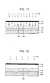
- FIGS. 1A to 1D are cross-sectional views illustrating a crystallization process according to an exemplary embodiment of the invention
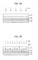
- FIGS. 2A to 2E are cross-sectional views illustrating a process of fabricating a thin film transistor according to an exemplary embodiment of the present invention.
- FIG. 3 is a cross-sectional view of an OLED display device according to an exemplary embodiment of the present invention.
- FIGS. 1A to 1D are cross-sectional views illustrating a crystallization process according to an exemplary embodiment of the present invention.
- a buffer layer 110 is formed on a substrate 100 such as glass or plastic as shown in FIG. 1A .
- the buffer layer 110 is formed of a single or double layer using an insulating layer such as a silicon oxide layer or a silicon nitride layer by a chemical vapor deposition (CVD) method or a physical vapor deposition (PVD) method.
- CVD chemical vapor deposition
- PVD physical vapor deposition
- the buffer layer 110 acts to prevent diffusion of moisture or impurities generated from the substrate 100 or acts to control a transfer rate of heat during crystallization, so that the crystallization of the amorphous silicon layer can be properly performed.
- a first amorphous silicon layer 120 is formed on the buffer layer 110.
- the first amorphous silicon layer 120 may be formed by CVD or PVD.
- a process of dehydrogenating the first amorphous silicon layer may be performed to reduce a hydrogen concentration.
- the first amorphous silicon layer 120 is crystallized into a first polycrystalline silicon layer.
- the first amorphous silicon layer 120 is crystallized into the first polycrystalline silicon layer by a crystallization method using a crystallization inducing metal such as an MIC method, an MILC method, or a super grained silicon (SGS) method.
- a crystallization inducing metal such as an MIC method, an MILC method, or a super grained silicon (SGS) method.
- a crystallization inducing metal such as nickel (Ni), palladium (Pd), aluminum (Al) or the like is in contact with or is implanted into an amorphous silicon layer to induce a phase change from the amorphous silicon layer into a polycrystalline silicon layer due to the crystallization inducing metal.
- the MILC method makes silicide generated by reacting a crystallization inducing metal with silicon laterally and continuously grow, and thereby to sequentially induce crystallization from an amorphous silicon layer into a polycrystalline silicon layer.
- FIG. 1B is a cross-sectional view illustrating a process of forming a capping layer and a crystallization inducing metal layer on the first amorphous silicon layer.
- a capping layer 130 is formed on the first amorphous silicon layer 120.
- the capping layer 130 is preferably formed of a silicon nitride layer which allows crystallization inducing metals to be formed in a subsequent process to be diffused through an annealing process, and may be formed of a double layer of a silicon nitride layer and a silicon oxide layer.
- the capping layer 130 is formed by a method such as CVD, PVD, or the like.
- the capping layer 130 has a thickness of 1 ⁇ to 2000 ⁇ .
- crystallization inducing metal is deposited on the capping layer 130 to form a crystallization inducing metal layer 140.
- the crystallization inducing metal may be one selected from the group consisting of Ni, Pd, Ti, Ag, Au, Al, Sn, Sb, Cu, Co, Mo, Zr, Ru, Rh, Cd, and Pt, preferably Ni.
- the crystallization inducing metal layer 140 is formed with a surface density of 10 11 atoms/cm 2 to 10 15 atoms/cm 2 on the capping layer 130.
- the crystallization inducing metals have a surface density less than 10 11 atoms/cm 2 , an amount of seed as a nucleus of crystallization is small so that it is difficult to crystallize the amorphous silicon layer into a polycrystalline silicon layer, and if the crystallization inducing metals have a surface density greater than 10 15 atoms/cm 2 an amount of crystallization inducing metal diffusing to the amorphous silicon layer is large so that crystal grains of the polycrystalline silicon layer are small, and an amount of remaining crystallization inducing metal is larger so that a characteristic of a semiconductor layer to be formed by patterning the polycrystalline silicon layer is deteriorated.
- the thickness of the crystallization inducing metal layer or density of the crystallization inducing metal should be carefully adjusted in the MIC or MILC method. This is because the crystallization inducing metals remain on a surface of the polycrystalline silicon layer after crystallization to cause a problem such as an increase in leakage current of the thin film transistor.
- the thick crystallization inducing metal layer may be formed without accurately controlling the thickness or density of the crystallization inducing metal layer in accordance with the present invention.
- FIG. 1C is a cross-sectional view illustrating a process of annealing the substrate to diffuse the crystallization inducing metal to an interface of the first amorphous silicon layer through the capping layer.
- the substrate 100 where the buffer layer 110, the first amorphous silicon layer 120, the capping layer 130, and the crystallization inducing metal layer 140 are formed is subjected to an annealing process 150 to move some of the metals of the crystallization inducing metal layer 140 to a surface of the first amorphous silicon layer 120.
- an amount of crystallization inducing metals reaching the surface of the first amorphous silicon layer 120 is determined by the diffusion suppressing ability of the capping layer 130, and the diffusion suppressing ability of the capping layer 130 has close relations with the thickness of the capping layer 130. That is, as the thickness of the capping layer 130 is thick, the amount of the diffused crystallization inducing metal decreases so that the size of a crystal grain is larger, and as the thickness of the capping layer 130 is thin, the amount of the diffused crystallization inducing metal increases so that the size of the crystal grain is smaller.
- the annealing process 150 is performed for several seconds to several hours at a temperature of 200°C to 900°C to diffuse the crystallization inducing metals, and may include one process of a furnace process, a rapid thermal annealing (RTA) process, a UV process, and a laser process.
- RTA rapid thermal annealing
- FIG. 1D is a cross-sectional view illustrating a process of crystallizing a first amorphous silicon layer into a first polycrystalline silicon layer due to diffused crystallization inducing metals.
- the first amorphous silicon layer 120 is crystallized into a first polycrystalline silicon layer 160 by the crystallization inducing metals 140b diffusing to the surface of the first amorphous silicon layer 120 through the capping layer 130. That is, the diffused crystallization inducing metals 140b are combined with silicon of the amorphous silicon layer to form metal silicide, and the metal silicide forms a seed as a nucleus of the crystallization so that the amorphous silicon layer is crystallized into the polycrystalline silicon layer.
- the crystallization method of the present invention includes forming a capping layer on an amorphous silicon layer, forming and annealing a metal catalyst layer on the capping layer, diffusing the metal catalyst, and crystallizing the amorphous silicon layer into a polycrystalline silicon layer using the diffused metal catalyst, which is referred to as an SGS crystallization method.
- an amount of the metal silicide as a nucleus of the crystallization i.e., an amount of the crystallization inducing metal 140b can be adjusted so that the crystal grain size of the first polycrystalline silicon layer 160 can be adjusted.
- the annealing process 150 was performed without removing the capping layer 130 and the crystallization inducing metal layer 140 in FIG. 1D .
- FIGS. 2A to 2E are cross-sectional views illustrating a process of fabricating a thin film transistor according to an exemplary embodiment of the present invention.
- a second amorphous silicon layer 170 is formed on the first polycrystalline silicon layer 160.
- the second amorphous silicon layer 170 may be formed by CVD or PVD.
- impurity ions 175 are implanted into the second amorphous silicon layer 170.
- P-type impurity ions or n-type impurity ions may be used as the impurity ions 175 for forming a thin film transistor.
- the p-type impurity may be selected from the group consisting of boron (B), aluminum (Al), gallium (Ga), and indium (In)
- the n-type impurity may be selected from the group consisting of phosphor (P), arsenic (As), and antimony (Sb).
- an annealing process 180 is performed to remove crystallization inducing metals (e.g., Ni) remaining in the first polycrystalline silicon layer 160.
- the annealing process 180 is preferably performed at a temperature of 500°C to 993°C for 30 seconds to 10 hours.
- the crystallization inducing metals (e.g., Ni) of the first polycrystalline silicon layer 160 does not occur to make it difficult to remove the crystallization inducing metals when the annealing process 180 is performed at a temperature below 500°C, and nickel having a eutectic point of 993°C may exist in a solid state at a temperature smaller than 993°C and the substrate 100 may be deformed due to high temperature when the annealing process 180 is performed at a temperature higher than 993°C.
- the crystallization inducing metals (e.g., Ni) of the first polycrystalline silicon layer 160 cannot be sufficiently removed when the annealing process 180 is performed for a time less than 30 seconds, and deformation of the substrate 100 and production cost and yield problems of the thin film transistor may be caused due to the annealing for a long time when the annealing process 180 is performed for a time exceeding 10 hours.
- the crystallization inducing metals 140b e.g., Ni
- the crystallization inducing metals 140b e.g., Ni
- the crystallization inducing metals 140b are diffused to the region where the second amorphous silicon layer 170 is formed due to the annealing process 180
- the crystallization inducing metals are precipitated so that they are not diffused any more.
- the crystallization inducing metals e.g., Ni
- the crystallization inducing metals e.g., Ni
- the crystallization inducing metals e.g., Ni
- the crystallization inducing metals e.g., Ni
- the crystallization inducing metals are diffused to the second amorphous silicon layer 170 by the annealing process 180 so that the second amorphous silicon layer 170 is crystallized into a second polycrystalline silicon layer by the crystallization inducing metals.
- the first polycrystalline silicon layer 160 and the second polycrystalline silicon layer are patterned to form a first semiconductor layer 190 and a second semiconductor layer, respectively.
- the second semiconductor layer 200 has an opening 200c exposing a portion of the first semiconductor layer 190.
- the second semiconductor layer 200 includes a source semiconductor layer 200a and a drain semiconductor layer 200b.
- the opening 200c is between the source semiconductor layer 200a and the drain semiconductor layer 200b.
- the second semiconductor layer includes a source semiconductor layer 200a and a drain semiconductor layer 200b.
- a material for source and drain electrodes is deposited on the entire surface of the substrate 100, and then patterned to form source and drain electrodes 210a and 210b. Accordingly, the source and drain electrodes 210a and 210b are electrically connected to the first semiconductor layer 190 and the second semiconductor layer 200. Specifically the source electrode 210a is connected to the source semiconductor layer 200a, and the drain electrode 210b is connected to the drain semiconductor layer 200b.
- a gate insulating layer 220 is formed on the entire surface of the substrate 100 to insulate its lower structures.
- the gate insulating layer 220 may be formed of a silicon nitride layer, a silicon oxide layer, or a multiple layer thereof.
- a gate electrode material is deposited on the entire surface of the substrate 100, and then patterned to form a gate electrode 230.
- the gate electrode 230 may be a single layer formed of Al or an aluminum alloy such as aluminum-neodymium (Al-Nd), or a multiple layer where an aluminum alloy is stacked on a Cr or Mo alloy.
- the gate electrode 230 is disposed on the gate insulating layer above the exposed portion of the first semiconductor layer. Accordingly, the source semiconductor layer 200a and a portion of the first semiconductor region 190 disposed below the source semiconductor layer 200a are a source region 191, and the drain semiconductor layer 200b and a portion of the first semiconductor region 190 disposed below the drain semiconductor layer 200b are a drain region 193.
- the exposed portion of the first semiconductor layer 190 below the gate electrode 230 can act as a channel region 192.
- an amorphous silicon layer is formed on a polycrystalline silicon layer subjected to a crystallization process using a crystallization inducing metal to remove the crystallization inducing metal remaining in the polycrystalline silicon layer, so that a thin film transistor capable of enhancing a leakage current characteristic of a semiconductor layer and an electrical characteristic can be provided.
- FIG. 3 is a cross-sectional view of an OLED display device according to an exemplary embodiment of the present invention.
- a planarization layer 240 is formed on the entire surface of the substrate 100.
- the planarization layer 240 may be formed of an organic layer, an inorganic layer, or a composite layer thereof.
- the planarization layer 240 is preferably formed a Spin-On-Glass (SOG) when it is formed of an inorganic layer, and preferably formed of an acrylic resin, a polyimide resin, or benzocyclobutene (BCB) when it is formed of an organic layer.
- SOG Spin-On-Glass
- BCB benzocyclobutene
- the planarization layer 240 and the gate insulating layer 220 are etched to form a via hole exposing one of the source and drain electrodes 210a and 210b, and a first electrode 250 is formed to be connected to one of the source and drain electrodes 210a and 210b.
- the first electrode 250 is disposed on the bottom of the via hole, is in contact with one of the source and drain electrodes 210a and 210b, and extends onto the planarization layer 240.
- the first electrode 250 may be formed of Indium Tin Oxide (ITO) or Indium Zinc Oxide (IZO).
- a pixel defining layer 260 is formed on the entire surface of the substrate 100 including the first electrode 250, wherein the pixel defining layer 260 has a thickness enough to sufficiently fill the via hole where the first electrode 250 is disposed.
- the pixel defining layer 260 may be formed of an organic layer or an inorganic layer, preferably an organic layer. More preferably, the pixel defining layer 260 is formed of one selected from the group consisting of benzocyclobutene (BCB), an acrylic polymer, and polyimide.
- BCB benzocyclobutene
- the pixel defining layer 260 has good flowability so that it can be smoothly formed on the entire surface of the substrate.
- the pixel defining layer 260 is etched to form an opening exposing the first electrode 250, and an organic layer 270 is formed on the first electrode 250 exposed through the opening.
- the organic layer 270 includes at least an emission layer, and may further include at least one of a hole injection layer, a hole transport layer, an electron transport layer, and an electron injection layer.
- a second electrode 280 is formed on the entire surface of the substrate 100.
- the second electrode 280 may be formed of Mg, Ag, Al, Ca, and an alloy thereof which is transparent as a transmissive electrode and has a low work function. Accordingly, an OLED display device according to an exemplary embodiment of the present invention is completed.
- a semiconductor layer formed of a polycrystalline silicon layer which is crystallized using nickel as a crystallization inducing metal an amorphous silicon layer is formed on the polycrystalline silicon layer and then subjected to annealing, and the nickel as the crystallization inducing metal is subjected to gettering, so that an amount of the crystallization inducing metal remaining in the polycrystalline silicon layer acting as a channel region of the semiconductor layer can be minimized and leakage current can be significantly reduced, thereby providing a thin film transistor having a good electrical characteristic and an OLED display device including the same.
- a thin film transistor having good leakage current and electrical characteristics by removing a crystallization inducing metal remaining in a semiconductor layer, a method of fabricating the same, and an OLED display device including the same can be provided.
Landscapes
- Physics & Mathematics (AREA)
- Geometry (AREA)
- Engineering & Computer Science (AREA)
- Microelectronics & Electronic Packaging (AREA)
- Recrystallisation Techniques (AREA)
- Thin Film Transistor (AREA)
- Electroluminescent Light Sources (AREA)
Applications Claiming Priority (1)
| Application Number | Priority Date | Filing Date | Title |
|---|---|---|---|
| KR1020060136781A KR100864884B1 (ko) | 2006-12-28 | 2006-12-28 | 박막트랜지스터, 그의 제조방법 및 이를 구비한유기전계발광표시장치 |
Publications (2)
| Publication Number | Publication Date |
|---|---|
| EP1939933A2 true EP1939933A2 (fr) | 2008-07-02 |
| EP1939933A3 EP1939933A3 (fr) | 2008-09-03 |
Family
ID=39301280
Family Applications (1)
| Application Number | Title | Priority Date | Filing Date |
|---|---|---|---|
| EP07124162A Ceased EP1939933A3 (fr) | 2006-12-28 | 2007-12-28 | Transistor à couche mince, son procédé de fabrication, et dispositif d'affichage de diode électroluminescente organique l'incluant |
Country Status (5)
| Country | Link |
|---|---|
| US (1) | US20080157116A1 (fr) |
| EP (1) | EP1939933A3 (fr) |
| JP (1) | JP2008166785A (fr) |
| KR (1) | KR100864884B1 (fr) |
| CN (1) | CN101211985A (fr) |
Cited By (2)
| Publication number | Priority date | Publication date | Assignee | Title |
|---|---|---|---|---|
| EP2204844A1 (fr) * | 2008-12-30 | 2010-07-07 | Samsung Mobile Display Co., Ltd. | Procédé de fabrication de silicium polycristallin, transistor à couche mince, son procédé de fabrication, et dispositif d'affichage à diode électroluminescente organique l'incluant |
| EP2325870A1 (fr) * | 2009-11-20 | 2011-05-25 | Samsung Mobile Display Co., Ltd. | Procédé de fabrication de couche en poly-silicone, transistor à film mince, dispositif électroluminescent organique l'incluant et son procédé de fabrication |
Families Citing this family (20)
| Publication number | Priority date | Publication date | Assignee | Title |
|---|---|---|---|---|
| KR101049806B1 (ko) | 2008-12-30 | 2011-07-15 | 삼성모바일디스플레이주식회사 | 다결정 실리콘의 제조방법, 박막트랜지스터, 그의 제조방법및 이를 포함하는 유기전계발광표시장치 |
| KR101015849B1 (ko) * | 2009-03-03 | 2011-02-23 | 삼성모바일디스플레이주식회사 | 박막트랜지스터, 그의 제조방법 및 이를 포함하는 유기전계발광표시장치 |
| KR101041141B1 (ko) | 2009-03-03 | 2011-06-13 | 삼성모바일디스플레이주식회사 | 유기전계발광표시장치 및 그의 제조방법 |
| KR101049801B1 (ko) | 2009-03-05 | 2011-07-15 | 삼성모바일디스플레이주식회사 | 다결정 실리콘층의 제조방법 및 이에 이용되는 원자층 증착장치 |
| KR101056428B1 (ko) | 2009-03-27 | 2011-08-11 | 삼성모바일디스플레이주식회사 | 박막트랜지스터, 그의 제조방법, 및 이를 포함하는 유기전계발광표시장치 |
| KR101094295B1 (ko) | 2009-11-13 | 2011-12-19 | 삼성모바일디스플레이주식회사 | 다결정 실리콘층의 제조방법, 박막트랜지스터의 제조방법, 및 유기전계발광표시장치의 제조방법 |
| KR101041147B1 (ko) | 2010-04-07 | 2011-06-13 | 삼성모바일디스플레이주식회사 | 박막 트랜지스터, 박막 트랜지스터의 액티브층의 제조 방법 및 표시 장치 |
| CN102254797A (zh) * | 2010-05-18 | 2011-11-23 | 京东方科技集团股份有限公司 | 低温多晶硅薄膜及其制造方法、晶体管和显示装置 |
| KR101146995B1 (ko) * | 2010-06-16 | 2012-05-22 | 삼성모바일디스플레이주식회사 | 다결정 실리콘층의 형성 방법 및 이를 이용한 박막 트랜지스터의 형성방법 |
| KR101720533B1 (ko) * | 2010-08-31 | 2017-04-03 | 삼성디스플레이 주식회사 | 다결정 실리콘층의 제조 방법, 상기 다결정 실리콘층 제조 방법을 포함하는 박막 트랜지스터의 제조 방법, 상기 방법에 의해 제조된 박막 트랜지스터, 및 상기 박막 트랜지스터를 포함하는 유기 발광 디스플레이 장치 |
| CN102013400A (zh) * | 2010-10-27 | 2011-04-13 | 四川虹视显示技术有限公司 | 生产底部金属结晶化的低温多晶硅薄膜晶体管的方法 |
| CN102629558B (zh) * | 2012-01-09 | 2015-05-20 | 深超光电(深圳)有限公司 | 低温多晶硅薄膜晶体管制造方法 |
| KR20140023491A (ko) * | 2012-08-16 | 2014-02-27 | 삼성코닝정밀소재 주식회사 | 스퍼터링 타겟 및 이에 의해 증착된 블랙 매트릭스를 포함하는 유기 발광 디스플레이 장치 |
| KR20140023492A (ko) * | 2012-08-16 | 2014-02-27 | 삼성코닝정밀소재 주식회사 | 스퍼터링 타겟 및 이에 의해 증착된 블랙 매트릭스를 포함하는 유기 발광 디스플레이 장치 |
| CN104716200B (zh) * | 2015-04-03 | 2018-01-09 | 京东方科技集团股份有限公司 | 薄膜晶体管及其制备方法、阵列基板和显示装置 |
| JP6367167B2 (ja) * | 2015-09-10 | 2018-08-01 | 東芝メモリ株式会社 | 半導体装置 |
| KR102527218B1 (ko) * | 2016-01-08 | 2023-04-28 | 삼성디스플레이 주식회사 | 유기 발광 표시 장치 및 그 제조 방법 |
| CN110212008B (zh) * | 2019-06-24 | 2021-07-23 | 深圳市华星光电半导体显示技术有限公司 | 阵列基板及其制备方法 |
| CN112420849B (zh) * | 2020-11-09 | 2024-08-20 | 昆山龙腾光电股份有限公司 | 金属氧化物薄膜晶体管及其制作方法 |
| KR20230168227A (ko) * | 2022-06-03 | 2023-12-13 | 삼성디스플레이 주식회사 | 표시 장치 |
Citations (1)
| Publication number | Priority date | Publication date | Assignee | Title |
|---|---|---|---|---|
| KR20030060403A (ko) | 2002-01-09 | 2003-07-16 | 장 진 | 비정질 실리콘의 결정화 방법 |
Family Cites Families (15)
| Publication number | Priority date | Publication date | Assignee | Title |
|---|---|---|---|---|
| KR980012633A (ko) * | 1996-07-25 | 1998-04-30 | 김광호 | 박막 트랜지스터의 제조방법 |
| US6218219B1 (en) * | 1997-09-29 | 2001-04-17 | Semiconductor Energy Laboratory Co., Ltd. | Semiconductor device and fabrication method thereof |
| US6346437B1 (en) * | 1998-07-16 | 2002-02-12 | Sharp Laboratories Of America, Inc. | Single crystal TFT from continuous transition metal delivery method |
| JP3425392B2 (ja) * | 1999-05-27 | 2003-07-14 | シャープ株式会社 | 半導体装置の製造方法 |
| JP2001135573A (ja) * | 1999-11-02 | 2001-05-18 | Sharp Corp | 半導体装置の製造方法およびその半導体装置 |
| US6695955B2 (en) * | 2001-05-25 | 2004-02-24 | Lg.Philips Lcd Co., Ltd. | Method of forming polycrystalline silicon for liquid crystal display device |
| US20060049428A1 (en) * | 2002-07-05 | 2006-03-09 | Van Der Zaag Pieter J | Tft electronic devices and their manufacture |
| US7348222B2 (en) * | 2003-06-30 | 2008-03-25 | Semiconductor Energy Laboratory Co., Ltd. | Method for manufacturing a thin film transistor and method for manufacturing a semiconductor device |
| KR100721555B1 (ko) * | 2004-08-13 | 2007-05-23 | 삼성에스디아이 주식회사 | 박막트랜지스터 및 그 제조 방법 |
| KR100656495B1 (ko) * | 2004-08-13 | 2006-12-11 | 삼성에스디아이 주식회사 | 박막트랜지스터 및 그 제조 방법 |
| KR100611762B1 (ko) * | 2004-08-20 | 2006-08-10 | 삼성에스디아이 주식회사 | 박막트랜지스터의 제조 방법 |
| KR100611766B1 (ko) * | 2004-08-24 | 2006-08-10 | 삼성에스디아이 주식회사 | 박막트랜지스터 제조 방법 |
| US7247529B2 (en) * | 2004-08-30 | 2007-07-24 | Semiconductor Energy Laboratory Co., Ltd. | Method for manufacturing display device |
| JP5030406B2 (ja) * | 2004-08-30 | 2012-09-19 | 株式会社半導体エネルギー研究所 | 表示装置の作製方法 |
| US7416928B2 (en) * | 2004-09-08 | 2008-08-26 | Semiconductor Energy Laboratory Co., Ltd. | Manufacturing method of semiconductor device |
-
2006
- 2006-12-28 KR KR1020060136781A patent/KR100864884B1/ko not_active Expired - Fee Related
-
2007
- 2007-12-25 JP JP2007332124A patent/JP2008166785A/ja active Pending
- 2007-12-28 US US12/003,618 patent/US20080157116A1/en not_active Abandoned
- 2007-12-28 EP EP07124162A patent/EP1939933A3/fr not_active Ceased
- 2007-12-28 CN CNA2007103066104A patent/CN101211985A/zh active Pending
Patent Citations (1)
| Publication number | Priority date | Publication date | Assignee | Title |
|---|---|---|---|---|
| KR20030060403A (ko) | 2002-01-09 | 2003-07-16 | 장 진 | 비정질 실리콘의 결정화 방법 |
Cited By (5)
| Publication number | Priority date | Publication date | Assignee | Title |
|---|---|---|---|---|
| EP2204844A1 (fr) * | 2008-12-30 | 2010-07-07 | Samsung Mobile Display Co., Ltd. | Procédé de fabrication de silicium polycristallin, transistor à couche mince, son procédé de fabrication, et dispositif d'affichage à diode électroluminescente organique l'incluant |
| US8507914B2 (en) | 2008-12-30 | 2013-08-13 | Samsung Display Co., Ltd. | Method of fabricating polysilicon, thin film transistor, method of fabricating the thin film transistor, and organic light emitting diode display device including the thin film transistor |
| EP2325870A1 (fr) * | 2009-11-20 | 2011-05-25 | Samsung Mobile Display Co., Ltd. | Procédé de fabrication de couche en poly-silicone, transistor à film mince, dispositif électroluminescent organique l'incluant et son procédé de fabrication |
| US9070717B2 (en) | 2009-11-20 | 2015-06-30 | Samsung Display Co., Ltd. | Method of fabricating polysilicon layer, thin film transistor, organic light emitting diode display device including the same, and method of fabricating the same |
| US9576797B2 (en) | 2009-11-20 | 2017-02-21 | Samsung Display Co., Ltd. | Method of fabricating polysilicon layer, thin film transistor, organic light emitting diode display device including the same, and method of fabricating the same |
Also Published As
| Publication number | Publication date |
|---|---|
| JP2008166785A (ja) | 2008-07-17 |
| EP1939933A3 (fr) | 2008-09-03 |
| KR100864884B1 (ko) | 2008-10-22 |
| CN101211985A (zh) | 2008-07-02 |
| US20080157116A1 (en) | 2008-07-03 |
| KR20080061734A (ko) | 2008-07-03 |
Similar Documents
| Publication | Publication Date | Title |
|---|---|---|
| EP1939933A2 (fr) | Transistor à couche mince, son procédé de fabrication, et dispositif d'affichage de diode électroluminescente organique l'incluant | |
| US8513669B2 (en) | Thin film transistor including metal or metal silicide structure in contact with semiconductor layer and organic light emitting diode display device having the thin film transistor | |
| US7825476B2 (en) | Method of fabricating polycrystalline silicon, TFT fabricated using the same, method of fabricating the TFT, and organic light emitting diode display device including the TFT | |
| EP2083440B1 (fr) | Procédé de fabrication de transistor à couche mince. | |
| EP2009680B1 (fr) | Procédé de fabrication d'une couche de silicone polycristallin | |
| US7838885B2 (en) | Thin film transistor, method of fabricating the thin film transistor, and display device including the thin film transistor | |
| EP2028687B1 (fr) | Procédé de fabrication de transistor à couche mince et dispositif d'affichage de diode électroluminescente organique l'incluant | |
| EP2146371B1 (fr) | Procédé de fabrication de transistor à couche mince | |
| EP2226848A1 (fr) | Transistor à couche mince, son procédé de fabrication et dispositif d'affichage à diode électroluminescente organique l'incluant | |
| US8198634B2 (en) | Thin film transistor, method of fabricating the same, and organic light emitting diode display device having the thin film transistor |
Legal Events
| Date | Code | Title | Description |
|---|---|---|---|
| PUAI | Public reference made under article 153(3) epc to a published international application that has entered the european phase |
Free format text: ORIGINAL CODE: 0009012 |
|
| 17P | Request for examination filed |
Effective date: 20071228 |
|
| AK | Designated contracting states |
Kind code of ref document: A2 Designated state(s): AT BE BG CH CY CZ DE DK EE ES FI FR GB GR HU IE IS IT LI LT LU LV MC MT NL PL PT RO SE SI SK TR |
|
| AX | Request for extension of the european patent |
Extension state: AL BA HR MK RS |
|
| PUAL | Search report despatched |
Free format text: ORIGINAL CODE: 0009013 |
|
| AK | Designated contracting states |
Kind code of ref document: A3 Designated state(s): AT BE BG CH CY CZ DE DK EE ES FI FR GB GR HU IE IS IT LI LT LU LV MC MT NL PL PT RO SE SI SK TR |
|
| AX | Request for extension of the european patent |
Extension state: AL BA HR MK RS |
|
| RAP1 | Party data changed (applicant data changed or rights of an application transferred) |
Owner name: SAMSUNG MOBILE DISPLAY CO., LTD. |
|
| AKX | Designation fees paid |
Designated state(s): DE FR GB |
|
| 17Q | First examination report despatched |
Effective date: 20090903 |
|
| RAP1 | Party data changed (applicant data changed or rights of an application transferred) |
Owner name: SAMSUNG DISPLAY CO., LTD. |
|
| STAA | Information on the status of an ep patent application or granted ep patent |
Free format text: STATUS: THE APPLICATION HAS BEEN REFUSED |
|
| 18R | Application refused |
Effective date: 20131212 |