EP2226848A1 - Transistor à couche mince, son procédé de fabrication et dispositif d'affichage à diode électroluminescente organique l'incluant - Google Patents
Transistor à couche mince, son procédé de fabrication et dispositif d'affichage à diode électroluminescente organique l'incluant Download PDFInfo
- Publication number
- EP2226848A1 EP2226848A1 EP20100154492 EP10154492A EP2226848A1 EP 2226848 A1 EP2226848 A1 EP 2226848A1 EP 20100154492 EP20100154492 EP 20100154492 EP 10154492 A EP10154492 A EP 10154492A EP 2226848 A1 EP2226848 A1 EP 2226848A1
- Authority
- EP
- European Patent Office
- Prior art keywords
- layer
- thin film
- film transistor
- metal catalyst
- disposed
- Prior art date
- Legal status (The legal status is an assumption and is not a legal conclusion. Google has not performed a legal analysis and makes no representation as to the accuracy of the status listed.)
- Ceased
Links
Images



Classifications
-
- H—ELECTRICITY
- H10—SEMICONDUCTOR DEVICES; ELECTRIC SOLID-STATE DEVICES NOT OTHERWISE PROVIDED FOR
- H10P—GENERIC PROCESSES OR APPARATUS FOR THE MANUFACTURE OR TREATMENT OF DEVICES COVERED BY CLASS H10
- H10P14/00—Formation of materials, e.g. in the shape of layers or pillars
- H10P14/20—Formation of materials, e.g. in the shape of layers or pillars of semiconductor materials
- H10P14/34—Deposited materials, e.g. layers
- H10P14/3402—Deposited materials, e.g. layers characterised by the chemical composition
- H10P14/3404—Deposited materials, e.g. layers characterised by the chemical composition being Group IVA materials
- H10P14/3411—Silicon, silicon germanium or germanium
-
- H—ELECTRICITY
- H10—SEMICONDUCTOR DEVICES; ELECTRIC SOLID-STATE DEVICES NOT OTHERWISE PROVIDED FOR
- H10D—INORGANIC ELECTRIC SEMICONDUCTOR DEVICES
- H10D30/00—Field-effect transistors [FET]
- H10D30/01—Manufacture or treatment
- H10D30/021—Manufacture or treatment of FETs having insulated gates [IGFET]
- H10D30/031—Manufacture or treatment of FETs having insulated gates [IGFET] of thin-film transistors [TFT]
- H10D30/0312—Manufacture or treatment of FETs having insulated gates [IGFET] of thin-film transistors [TFT] characterised by the gate electrodes
- H10D30/0314—Manufacture or treatment of FETs having insulated gates [IGFET] of thin-film transistors [TFT] characterised by the gate electrodes of lateral top-gate TFTs comprising only a single gate
-
- H—ELECTRICITY
- H10—SEMICONDUCTOR DEVICES; ELECTRIC SOLID-STATE DEVICES NOT OTHERWISE PROVIDED FOR
- H10D—INORGANIC ELECTRIC SEMICONDUCTOR DEVICES
- H10D30/00—Field-effect transistors [FET]
- H10D30/01—Manufacture or treatment
- H10D30/021—Manufacture or treatment of FETs having insulated gates [IGFET]
- H10D30/031—Manufacture or treatment of FETs having insulated gates [IGFET] of thin-film transistors [TFT]
- H10D30/0321—Manufacture or treatment of FETs having insulated gates [IGFET] of thin-film transistors [TFT] comprising silicon, e.g. amorphous silicon or polysilicon
-
- H—ELECTRICITY
- H10—SEMICONDUCTOR DEVICES; ELECTRIC SOLID-STATE DEVICES NOT OTHERWISE PROVIDED FOR
- H10D—INORGANIC ELECTRIC SEMICONDUCTOR DEVICES
- H10D30/00—Field-effect transistors [FET]
- H10D30/60—Insulated-gate field-effect transistors [IGFET]
- H10D30/67—Thin-film transistors [TFT]
- H10D30/6729—Thin-film transistors [TFT] characterised by the electrodes
- H10D30/673—Thin-film transistors [TFT] characterised by the electrodes characterised by the shapes, relative sizes or dispositions of the gate electrodes
- H10D30/6731—Top-gate only TFTs
-
- H—ELECTRICITY
- H10—SEMICONDUCTOR DEVICES; ELECTRIC SOLID-STATE DEVICES NOT OTHERWISE PROVIDED FOR
- H10D—INORGANIC ELECTRIC SEMICONDUCTOR DEVICES
- H10D30/00—Field-effect transistors [FET]
- H10D30/60—Insulated-gate field-effect transistors [IGFET]
- H10D30/67—Thin-film transistors [TFT]
- H10D30/674—Thin-film transistors [TFT] characterised by the active materials
- H10D30/6741—Group IV materials, e.g. germanium or silicon carbide
- H10D30/6743—Silicon
- H10D30/6745—Polycrystalline or microcrystalline silicon
-
- H—ELECTRICITY
- H10—SEMICONDUCTOR DEVICES; ELECTRIC SOLID-STATE DEVICES NOT OTHERWISE PROVIDED FOR
- H10D—INORGANIC ELECTRIC SEMICONDUCTOR DEVICES
- H10D30/00—Field-effect transistors [FET]
- H10D30/60—Insulated-gate field-effect transistors [IGFET]
- H10D30/67—Thin-film transistors [TFT]
- H10D30/6758—Thin-film transistors [TFT] characterised by the insulating substrates
-
- H—ELECTRICITY
- H10—SEMICONDUCTOR DEVICES; ELECTRIC SOLID-STATE DEVICES NOT OTHERWISE PROVIDED FOR
- H10D—INORGANIC ELECTRIC SEMICONDUCTOR DEVICES
- H10D86/00—Integrated devices formed in or on insulating or conducting substrates, e.g. formed in silicon-on-insulator [SOI] substrates or on stainless steel or glass substrates
- H10D86/01—Manufacture or treatment
- H10D86/021—Manufacture or treatment of multiple TFTs
- H10D86/0221—Manufacture or treatment of multiple TFTs comprising manufacture, treatment or patterning of TFT semiconductor bodies
- H10D86/0223—Manufacture or treatment of multiple TFTs comprising manufacture, treatment or patterning of TFT semiconductor bodies comprising crystallisation of amorphous, microcrystalline or polycrystalline semiconductor materials
- H10D86/0225—Manufacture or treatment of multiple TFTs comprising manufacture, treatment or patterning of TFT semiconductor bodies comprising crystallisation of amorphous, microcrystalline or polycrystalline semiconductor materials using crystallisation-promoting species, e.g. using a Ni catalyst
-
- H—ELECTRICITY
- H10—SEMICONDUCTOR DEVICES; ELECTRIC SOLID-STATE DEVICES NOT OTHERWISE PROVIDED FOR
- H10D—INORGANIC ELECTRIC SEMICONDUCTOR DEVICES
- H10D86/00—Integrated devices formed in or on insulating or conducting substrates, e.g. formed in silicon-on-insulator [SOI] substrates or on stainless steel or glass substrates
- H10D86/40—Integrated devices formed in or on insulating or conducting substrates, e.g. formed in silicon-on-insulator [SOI] substrates or on stainless steel or glass substrates characterised by multiple TFTs
-
- H—ELECTRICITY
- H10—SEMICONDUCTOR DEVICES; ELECTRIC SOLID-STATE DEVICES NOT OTHERWISE PROVIDED FOR
- H10P—GENERIC PROCESSES OR APPARATUS FOR THE MANUFACTURE OR TREATMENT OF DEVICES COVERED BY CLASS H10
- H10P14/00—Formation of materials, e.g. in the shape of layers or pillars
- H10P14/20—Formation of materials, e.g. in the shape of layers or pillars of semiconductor materials
- H10P14/29—Formation of materials, e.g. in the shape of layers or pillars of semiconductor materials characterised by the substrates
- H10P14/2901—Materials
- H10P14/2922—Materials being non-crystalline insulating materials, e.g. glass or polymers
-
- H—ELECTRICITY
- H10—SEMICONDUCTOR DEVICES; ELECTRIC SOLID-STATE DEVICES NOT OTHERWISE PROVIDED FOR
- H10P—GENERIC PROCESSES OR APPARATUS FOR THE MANUFACTURE OR TREATMENT OF DEVICES COVERED BY CLASS H10
- H10P14/00—Formation of materials, e.g. in the shape of layers or pillars
- H10P14/20—Formation of materials, e.g. in the shape of layers or pillars of semiconductor materials
- H10P14/32—Formation of materials, e.g. in the shape of layers or pillars of semiconductor materials characterised by intermediate layers between substrates and deposited layers
- H10P14/3202—Materials thereof
- H10P14/3238—Materials thereof being insulating materials
-
- H—ELECTRICITY
- H10—SEMICONDUCTOR DEVICES; ELECTRIC SOLID-STATE DEVICES NOT OTHERWISE PROVIDED FOR
- H10P—GENERIC PROCESSES OR APPARATUS FOR THE MANUFACTURE OR TREATMENT OF DEVICES COVERED BY CLASS H10
- H10P14/00—Formation of materials, e.g. in the shape of layers or pillars
- H10P14/20—Formation of materials, e.g. in the shape of layers or pillars of semiconductor materials
- H10P14/38—Formation of materials, e.g. in the shape of layers or pillars of semiconductor materials characterised by treatments done after the formation of the materials
- H10P14/3802—Crystallisation or recrystallisation of non-monocrystalline semiconductor materials, e.g. regrowth
- H10P14/3806—Crystallisation or recrystallisation of non-monocrystalline semiconductor materials, e.g. regrowth using crystallisation-enhancing elements
Definitions
- the present invention relates to a thin film transistor, a method of fabricating the same, and an organic light emitting diode display device having the same.
- polysilicon layers are widely used as semiconductor layers of thin film transistors, due to having high field effect mobility, and applicability to high-speed operation circuits and complementary metal-oxide semiconductor (CMOS) circuits.
- CMOS complementary metal-oxide semiconductor
- Thin film transistors including polysilicon layers are mainly used as active elements of active matrix liquid crystal displays and as switching devices, or driving elements, of organic light emitting diode display devices.
- Methods of crystallizing amorphous silicon into polysilicon include a solid-phase crystallization method, an excimer laser crystallization method, a metal-induced crystallization method, and a metal-induced lateral crystallization method.
- a solid-phase crystallization method an amorphous silicon layer is annealed for from several hours, to tens of hours, at a temperature of about 700° C, or less, which is the deformation temperature of glass that is used as the substrate of a display device in which a TFT is used.
- the excimer laser crystallization method crystallization is carried out by irradiating an excimer laser onto an amorphous silicon layer, for a very short time, to locally heat the layer.
- a phase change from an amorphous silicon layer into a polycrystalline silicon layer is induced by a metal, such as nickel, palladium, gold, or aluminum, by contacting the amorphous silicon layer with the metal, or by implanting the metal into the amorphous silicon layer.
- a metal such as nickel, palladium, gold, or aluminum
- sequential crystallization of an amorphous silicon layer is induced, while a silicide generated by the reaction between metal and silicon propagates laterally.
- the solid-phase crystallization method requires a long processing time and a long annealing time at a high temperature, so a substrate is disadvantageously apt to be deformed.
- the excimer laser crystallization method requires a costly laser apparatus and causes imperfections on a polycrystallized surface, providing an inferior interface between a semiconductor layer and a gate insulating layer.
- Crystallization methods using a metal include a metal-induced crystallization (MIC) method, a metal-induced lateral crystallization (MILC) method, and a super grain silicon (SGS) crystallization method.
- MIC metal-induced crystallization
- MILC metal-induced lateral crystallization
- SGS super grain silicon
- One of the determining characteristics of a thin film transistor is a leakage current.
- the metal catalyst may remain in a channel region, and thus, increase a leakage current. Therefore, if the concentration of the metal catalyst remaining in the channel region is not controlled, the leakage current of the thin film transistor may increase, leading to degradation of the electrical characteristics thereof.
- aspects of the present invention provide a thin film transistor including a semiconductor layer that is crystallized using a metal catalyst, which has a reduced amount of residual metal catalyst remaining in the semiconductor layer, a method of fabricating the same, and an organic light emitting diode display device including the same.
- a thin film transistor that includes: a substrate; a silicon layer formed on the substrate; a diffusion layer formed on the silicon layer; a semiconductor layer formed on the diffusion layer, which is crystallized using a metal catalyst; a gate electrode disposed on a channel region of the semiconductor layer; a gate insulating layer disposed between the gate electrode and the semiconductor layer; and source and drain electrodes electrically connected to source and drain regions of the semiconductor layer.
- a method of fabricating the thin film transistor that includes: forming a silicon layer on a substrate; forming a diffusion layer on the silicon layer; forming an amorphous silicon layer on the diffusion layer; forming a metal catalyst layer on the amorphous silicon layer; annealing the substrate to convert the amorphous silicon layer into a polysilicon layer; removing the metal catalyst layer; patterning the amorphous silicon layer to form a semiconductor layer; forming a gate insulating layer on the substrate; forming a gate electrode that faces the semiconductor layer; forming an interlayer insulating layer on the substrate; and forming source and drain electrodes that are connected to the semiconductor layer.
- an organic light emitting diode display device that includes: a substrate; a silicon layer formed on the substrate; a diffusion layer formed on the silicon layer; a semiconductor layer that is crystallized using a metal catalyst, formed on the diffusion layer; a gate electrode disposed on a channel region of the semiconductor layer; a gate insulating layer disposed between the gate electrode and the semiconductor layer; source and drain electrodes electrically connected to the semiconductor layer; a passivation layer disposed on the substrate; and a first electrode, an organic layer, and a second electrode disposed on the passivation layer and electrically connected to one of the source and drain electrodes, with the organic layer being disposed between the first and second electrodes.
- first element when a first element is referred to as being formed or disposed "on" a second element, the first element can be disposed directly on the second element, or one or more other elements may be disposed therebetween.
- first element when referred to as being formed or disposed "directly on” a second element, no other elements are disposed therebetween.
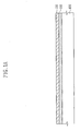
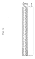
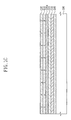
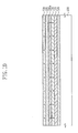
- FIGS. 1A to 1F are cross-sectional views of a thin film transistor, in accordance with an exemplary embodiment of the present invention.
- a buffer layer 105 is formed on a glass or plastic substrate 100.
- the buffer layer 105 is an insulating layer, such as a silicon oxide layer or a silicon nitride layer, or multiple layers thereof.
- the buffer layer 105 can be formed using a chemical vapor deposition method or a physical vapor deposition method.
- the buffer layer 105 prevents the diffusion of moisture and/or impurities from the substrate 100, and/or adjusts a heat transfer rate to facilitate the crystallization of an amorphous silicon layer.
- a silicon layer 110 is formed on the buffer layer 105.
- the silicon layer 110 is formed of amorphous silicon, using a chemical vapor deposition method or a physical vapor deposition method.
- a diffusion layer 115 is formed on the silicon layer 110.
- the diffusion layer 115 may be formed of a silicon nitride layer, in which a metal catalyst can be diffused through an annealing process.
- the diffusion layer 115 may be formed of stacked silicon nitride and silicon oxide layers.
- An amorphous silicon layer 120a is formed on the diffusion layer 115.
- the amorphous silicon layer 120a may be formed by a chemical vapor deposition method or a physical vapor deposition method.
- dehydrogenation may be performed during or after the formation of the amorphous silicon layer 120a, to reduce the concentration of hydrogen therein.
- the amorphous silicon layer 120a is crystallized into a polysilicon layer (not shown), using metal catalyst a crystallization method.
- the method can be, for example, a metal-induced crystallization (MIC) method, a metal-induced lateral crystallization (MILC) method, or a super grain silicon (SGS) crystallization method.
- MIC metal-induced crystallization
- MILC metal-induced lateral crystallization
- SGS super grain silicon
- the SGS crystallization method is capable of reducing the concentration of a metal catalyst that is diffused into an amorphous silicon layer, to adjust the grain size produced thereby, to from several ⁇ m to several hundreds of ⁇ m.
- a metal catalyst layer may be formed on the diffusion layer, which is then annealed to diffuse the metal catalyst.
- the concentration of the metal catalyst may also be reduced without including the diffusion layer, by forming the metal catalyst layer at a low concentration, directly on the amorphous silicon layer.
- a capping layer 125 is formed on the amorphous silicon layer 120a.
- the capping layer 125 may be a silicon nitride layer, in which a metal catalyst can be diffused through annealing, or may include stacked silicon nitride and silicon oxide layers.
- the capping layer 125 can be formed by a chemical vapor deposition method or a physical vapor deposition method.
- the capping layer 125 may have a thickness of from about 0.1 to 200nm (2000 ⁇ ). When the thickness of the capping layer 125 is less than about 0.1nm (1 ⁇ ), it may be difficult to reduce the amount of the metal catalyst diffused in the capping layer 125.
- the thickness of the capping layer 125 is larger than about 200nm (2000 ⁇ ), it may be difficult to crystallize the amorphous silicon layer 120a into the polysilicon layer, because the amount of the metal catalyst diffused into the amorphous silicon layer 120a is small.
- a metal catalyst layer 130 is deposited on the capping layer 125.
- the metal catalyst layer 130 may be formed of a metal catalyst selected from the group consisting of Ni, Pd, Ag, Au, Al, Sn, Sb, Cu, Ti, and Cd.
- the metal catalyst layer 130 is generally formed with an areal density of from about 1011 to 1015 atoms/cm 2 . When the areal density of the metal catalyst layer 130 is less than about 1011 atoms/cm 2 , it may be difficult to crystallize the amorphous silicon layer 120a by SGS crystallization, because the amount of crystallization seeds is small.
- the areal density of the metal catalyst layer 130 is more than about 1015 atoms/cm 2 , the amount of the metal catalyst diffused into the amorphous silicon layer 120a is increased, reducing the grain size of the polysilicon layer formed from the amorphous silicon layer 120a. In addition, the amount of the metal catalyst remaining after crystallization is increased, which may deteriorate the characteristics of a semiconductor layer formed by patterning the polysilicon layer.
- the substrate 100 on which the buffer layer 105, the silicon layer 110, the diffusion layer 115, the amorphous silicon layer 120a, the capping layer 125, and the metal catalyst layer 130 are formed, is annealed to diffuse some of the metal catalyst of the metal catalyst layer 130 into the surface of the amorphous silicon layer 120a. That is, the capping layer 125 acts to impede the diffusion of the metal catalyst into the surface of the amorphous silicon layer 120a.
- the amount of the metal catalyst diffused into the amorphous silicon layer 120a is determined by the diffusion characteristics of the diffusion layer 115 and the diffusion characteristics of the capping layer 125, which is closely related to the thickness of the capping layer 125. That is, an increase in thickness of the capping layer 125 reduces diffusion and increases the grain size of the resultant polysilicon layer, and a reduction in thickness of the capping layer 125 increases the diffusion and reduces the grain size of the polysilicon layer.
- the metal catalyst arriving at the amorphous silicon layer 120a is diffused into the diffusion layer 115 and the silicon layer 110. Therefore, the amount of the metal catalyst in the amorphous silicon layer 120a is reduced, to provide a gettering effect.
- FIG. 3A is a graph showing the concentrations of a metal catalyst when only a buffer layer is disposed under an amorphous silicon layer
- FIG. 3B is a graph showing concentrations of a metal catalyst when a diffusion layer and a silicon layer are disposed under an amorphous silicon layer.
- the metal catalyst arriving at the silicon layer 110 is used to crystallize the silicon layer 110, in the same manner as in the crystallization of the amorphous silicon layer 120a into the polysilicon layer.
- the grains of the silicon layer 110 are secondary grains crystallized by the metal catalyst diffused from the amorphous silicon layer 120a.
- the grains of the silicon layer 110 are larger than the grains in the amorphous silicon layer 120a, have indistinct grain boundaries, and thus, are different from the grains of the amorphous silicon layer 120a.
- the annealing is performed at a temperature of from about 200 to 900 °C, and in particular, from about 350 to 500 °C, for several seconds to several hours, to diffuse the metal catalyst.
- the annealing may be one of a furnace process, a rapid thermal annealing (RTA) process, an ultraviolet (UV) process, and a laser process.
- RTA rapid thermal annealing
- UV ultraviolet
- the polysilicon layer formed in the above manner is patterned to form a semiconductor layer 120.
- a gate insulating layer 140 is formed on the semiconductor layer 120 and the diffusion layer 115.
- a gate electrode 150 is formed on the gate insulating layer 140, adjacent to the semiconductor layer 120.
- the gate insulating layer 140 may include a silicon oxide layer, a silicon nitride layer, or stacked layers thereof.
- a metal layer (not shown) is then formed on the gate insulating layer 140.
- the metal layer can be a single layer of aluminum (Al) or an aluminum alloy such as aluminum-neodymium (Al-Nd), or a multi-layer, in which an aluminum alloy is deposited on a chrome (Cr) or molybdenum (Mo) alloy.
- the metal layer is etched through a photolithography process, to form a gate electrode 150 that faces a portion of the semiconductor layer 120, the portion comprising a channel region in the finished thin film transistor.
- an interlayer insulating layer 160 is formed on the gate insulating layer 140 and the gate electrode 150.
- the interlayer insulating layer 160 may be a silicon nitride layer, a silicon oxide layer, or stacked layers thereof.
- the interlayer insulating layer 160 and the gate insulating layer 140 are etched to form contact holes exposing portions of the semiconductor layer 120.
- Source and drain electrodes 170a and 170b are formed on the interlayer insulating layer 160 and connected to the source and drain regions through the contact holes, completing the thin film transistor.
- the source and drain electrodes 170a and 170b may be formed of one selected from molybdenum (Mo), chrome (Cr), tungsten (W), molybdenum tungsten (MoW), aluminum (Al), aluminum-neodymium (Al-Nd), titanium (Ti), titanium nitride (TiN), copper (Cu), a molybdenum (Mo) alloy, an aluminum (Al) alloy, and a copper (Co) alloy.
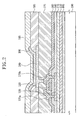
- FIG. 2 is a cross-sectional view of an organic light emitting diode display device, in accordance with another exemplary embodiment of the present invention.
- the light emitting diode display device includes the thin film transistor of FIG. 1F , and thus, descriptions of similar elements are omitted.
- a passivation layer 175 is formed on the source and drain electrodes 170a and 170b, and the interlayer insulating layer 160.
- the passivation layer 175 may be an inorganic layer, such as a silicon oxide layer, a silicon nitride layer, or silicon on glass (SOG) layer.
- passivation layer 175 may be an organic layer, such as a polyimide layer, a benzocyclobutene series resin layer, or an acrylate layer.
- the passivation layer 175 may be a stack formed of the inorganic layer and the organic layer.
- the passivation layer 175 is etched to form a hole exposing the drain electrode 170b.
- a first electrode 180 is connected to the drain electrode 170b, through the hole.
- the first electrode 180 may be referred to as an anode or a cathode.
- the anode may be a transparent conductive layer formed of one selected from indium tin oxide (ITO), indium zinc oxide (IZO), and indium tin zinc oxide (ITZO).
- ITO indium tin oxide
- IZO indium zinc oxide
- ITZO indium tin zinc oxide
- the cathode may be formed of Mg, Ca, Al, Ag, Ba, or an alloy thereof.
- the hole in the passivation layer 175 may expose the source electrode 170a, and the first electrode 180 may be connected to the source electrode 170a, via the hole.
- a pixel defining layer 185 having an opening exposing the first electrode 180, is formed on the first electrode 180 and the passivation layer 175.
- An organic layer 190 is formed on the exposed first electrode 180.
- the organic layer 190 includes including an emission layer and may include at least one layer selected from a hole injection layer, a hole transport layer, a hole blocking layer, an electron blocking layer, an electron injection layer, and an electron transport layer.
- a second electrode 195 is formed on the organic layer 190. As a result, the organic light emitting diode display device is completed.
- the present invention may be applied to a thin film transistor having a bottom gate structure, including: a substrate; a gate electrode disposed on the substrate; a gate insulating layer disposed on the substrate; a silicon layer disposed on the substrate; a diffusion layer disposed on the silicon layer; a semiconductor layer disposed on the diffusion layer; and source and drain electrodes for opening a portion of the semiconductor layer and connected to the semiconductor layer, and an organic light emitting diode display device having the same.
- aspects of the present invention provide a thin film transistor having a semiconductor layer that is crystallized using a metal catalyst, a method of fabricating the same, and an organic light emitting diode display device having the same.
- the semiconductor layer has a larger grain size and a smaller amount of residual metal than a conventional semiconductor layer.
- the thin film transistor has an improved threshold voltage and Ioff characteristics.
Landscapes
- Recrystallisation Techniques (AREA)
- Thin Film Transistor (AREA)
- Electroluminescent Light Sources (AREA)
Applications Claiming Priority (1)
| Application Number | Priority Date | Filing Date | Title |
|---|---|---|---|
| KR1020090018199A KR101049799B1 (ko) | 2009-03-03 | 2009-03-03 | 박막트랜지스터, 그의 제조방법 및 이를 포함하는 유기전계발광표시장치 |
Publications (1)
| Publication Number | Publication Date |
|---|---|
| EP2226848A1 true EP2226848A1 (fr) | 2010-09-08 |
Family
ID=42174000
Family Applications (1)
| Application Number | Title | Priority Date | Filing Date |
|---|---|---|---|
| EP20100154492 Ceased EP2226848A1 (fr) | 2009-03-03 | 2010-02-24 | Transistor à couche mince, son procédé de fabrication et dispositif d'affichage à diode électroluminescente organique l'incluant |
Country Status (5)
| Country | Link |
|---|---|
| US (1) | US20100224882A1 (fr) |
| EP (1) | EP2226848A1 (fr) |
| JP (1) | JP5527874B2 (fr) |
| KR (1) | KR101049799B1 (fr) |
| CN (1) | CN101826555B (fr) |
Families Citing this family (10)
| Publication number | Priority date | Publication date | Assignee | Title |
|---|---|---|---|---|
| KR101041141B1 (ko) | 2009-03-03 | 2011-06-13 | 삼성모바일디스플레이주식회사 | 유기전계발광표시장치 및 그의 제조방법 |
| KR101809661B1 (ko) * | 2011-06-03 | 2017-12-18 | 삼성디스플레이 주식회사 | 박막 트랜지스터, 그 제조 방법 및 이를 포함하는 유기 발광 표시 장치 |
| KR101903445B1 (ko) * | 2012-01-10 | 2018-10-05 | 삼성디스플레이 주식회사 | 반도체 장치 및 이의 제조 방법 |
| TWI529939B (zh) * | 2012-02-08 | 2016-04-11 | 新力股份有限公司 | High frequency semiconductor device and its manufacturing method |
| KR20140039863A (ko) * | 2012-09-25 | 2014-04-02 | 삼성디스플레이 주식회사 | 다결정 규소막 형성 방법, 다결정 규소막을 포함하는 박막 트랜지스터 및 표시 장치 |
| CN104716024A (zh) * | 2015-03-04 | 2015-06-17 | 山东大学 | 一种提升薄膜半导体晶体管电学性能的方法 |
| US9966301B2 (en) | 2016-06-27 | 2018-05-08 | New Fab, LLC | Reduced substrate effects in monolithically integrated RF circuits |
| US10062636B2 (en) | 2016-06-27 | 2018-08-28 | Newport Fab, Llc | Integration of thermally conductive but electrically isolating layers with semiconductor devices |
| WO2018043643A1 (fr) * | 2016-09-02 | 2018-03-08 | シャープ株式会社 | Substrat de matrice active et dispositif d'affichage muni d'un substrat de matrice active |
| US20260032965A1 (en) * | 2024-07-25 | 2026-01-29 | Zinite Corporation | Thin-film transistors and related methods of manufacture with metal nitride source/drain |
Citations (4)
| Publication number | Priority date | Publication date | Assignee | Title |
|---|---|---|---|---|
| US20020063261A1 (en) * | 1993-06-24 | 2002-05-30 | Hongyong Zhang | Semiconductor device and process for fabricating the same |
| US20050184290A1 (en) * | 1999-05-10 | 2005-08-25 | Semiconductor Energy Laboratory Co., Ltd. | Semiconductor device |
| US20060051914A1 (en) * | 2004-09-08 | 2006-03-09 | Semiconductor Energy Laboratory Co., Ltd. | Manufacturing method of semiconductor device |
| US20090050894A1 (en) * | 2007-08-22 | 2009-02-26 | Samsung Sdi Co., Ltd. | Thin film transistor, method of fabricating the same, organic light emitting diode display device haing the tft, and method of fabricating the oled display device |
Family Cites Families (37)
| Publication number | Priority date | Publication date | Assignee | Title |
|---|---|---|---|---|
| EP0589049B1 (fr) * | 1992-03-25 | 2000-01-12 | Kanegafuchi Chemical Industry Co., Ltd. | Couche mince de polysilicium et sa fabrication |
| JPH0669515A (ja) * | 1992-08-19 | 1994-03-11 | Fujitsu Ltd | 半導体記憶装置 |
| JP3107941B2 (ja) * | 1993-03-05 | 2000-11-13 | 株式会社半導体エネルギー研究所 | 薄膜トランジスタおよびその作製方法 |
| US7081938B1 (en) * | 1993-12-03 | 2006-07-25 | Semiconductor Energy Laboratory Co., Ltd. | Electro-optical device and method for manufacturing the same |
| TW317643B (fr) * | 1996-02-23 | 1997-10-11 | Handotai Energy Kenkyusho Kk | |
| JPH1174536A (ja) * | 1997-01-09 | 1999-03-16 | Sanyo Electric Co Ltd | 半導体装置の製造方法 |
| JP2000031488A (ja) * | 1997-08-26 | 2000-01-28 | Semiconductor Energy Lab Co Ltd | 半導体装置およびその作製方法 |
| JP3706527B2 (ja) * | 1999-06-30 | 2005-10-12 | Hoya株式会社 | 電子線描画用マスクブランクス、電子線描画用マスクおよび電子線描画用マスクの製造方法 |
| JP3715848B2 (ja) * | 1999-09-22 | 2005-11-16 | シャープ株式会社 | 半導体装置の製造方法 |
| US6294442B1 (en) * | 1999-12-10 | 2001-09-25 | National Semiconductor Corporation | Method for the formation of a polysilicon layer with a controlled, small silicon grain size during semiconductor device fabrication |
| GB2358081B (en) * | 2000-01-07 | 2004-02-18 | Seiko Epson Corp | A thin-film transistor and a method for maufacturing thereof |
| KR100387122B1 (ko) * | 2000-09-15 | 2003-06-12 | 피티플러스(주) | 백 바이어스 효과를 갖는 다결정 실리콘 박막 트랜지스터의 제조 방법 |
| JP2003100629A (ja) * | 2001-09-19 | 2003-04-04 | Sharp Corp | 半導体装置及びその製造方法 |
| JP4135347B2 (ja) * | 2001-10-02 | 2008-08-20 | 株式会社日立製作所 | ポリシリコン膜生成方法 |
| US6933527B2 (en) * | 2001-12-28 | 2005-08-23 | Semiconductor Energy Laboratory Co., Ltd. | Semiconductor device and semiconductor device production system |
| TW536716B (en) * | 2002-07-04 | 2003-06-11 | Ind Tech Res Inst | Capacitor structure of low temperature polysilicon |
| JP4092261B2 (ja) * | 2002-08-02 | 2008-05-28 | 三星エスディアイ株式会社 | 基板の製造方法及び有機エレクトロルミネッセンス素子の製造方法 |
| KR100470274B1 (ko) * | 2002-11-08 | 2005-02-05 | 진 장 | 덮개층을 이용한 비정질 물질의 상 변화 방법 |
| JP4115252B2 (ja) * | 2002-11-08 | 2008-07-09 | シャープ株式会社 | 半導体膜およびその製造方法ならびに半導体装置およびその製造方法 |
| TWI305681B (en) * | 2002-11-22 | 2009-01-21 | Toppoly Optoelectronics Corp | Method for fabricating thin film transistor array and driving circuits |
| JP4059095B2 (ja) * | 2003-02-07 | 2008-03-12 | セイコーエプソン株式会社 | 相補型薄膜トランジスタ回路、電気光学装置、電子機器 |
| US7238963B2 (en) * | 2003-04-28 | 2007-07-03 | Tpo Displays Corp. | Self-aligned LDD thin-film transistor and method of fabricating the same |
| US7358165B2 (en) * | 2003-07-31 | 2008-04-15 | Semiconductor Energy Laboratory Co., Ltd | Semiconductor device and method for manufacturing semiconductor device |
| US8114719B2 (en) * | 2004-06-03 | 2012-02-14 | Semiconductor Energy Laboratory Co., Ltd. | Memory device and manufacturing method of the same |
| KR100600874B1 (ko) * | 2004-06-09 | 2006-07-14 | 삼성에스디아이 주식회사 | 박막트랜지스터 및 그의 제조 방법 |
| KR100611659B1 (ko) * | 2004-07-07 | 2006-08-10 | 삼성에스디아이 주식회사 | 박막트랜지스터 및 그의 제조 방법 |
| KR100656495B1 (ko) * | 2004-08-13 | 2006-12-11 | 삼성에스디아이 주식회사 | 박막트랜지스터 및 그 제조 방법 |
| KR100611764B1 (ko) * | 2004-08-20 | 2006-08-10 | 삼성에스디아이 주식회사 | 박막트랜지스터의 제조 방법 |
| KR100611766B1 (ko) * | 2004-08-24 | 2006-08-10 | 삼성에스디아이 주식회사 | 박막트랜지스터 제조 방법 |
| KR20060026776A (ko) * | 2004-09-21 | 2006-03-24 | 삼성에스디아이 주식회사 | 유기 전계 발광 소자 및 그의 제조 방법 |
| JP5073482B2 (ja) * | 2005-03-31 | 2012-11-14 | 東京エレクトロン株式会社 | シリコン酸化膜の製造方法、その制御プログラム、記憶媒体及びプラズマ処理装置 |
| US7341907B2 (en) * | 2005-04-05 | 2008-03-11 | Applied Materials, Inc. | Single wafer thermal CVD processes for hemispherical grained silicon and nano-crystalline grain-sized polysilicon |
| US20080258186A1 (en) * | 2005-12-19 | 2008-10-23 | Nxp B.V. | Source and Drain Formation in Silicon on Insulator Device |
| KR100770266B1 (ko) * | 2006-11-10 | 2007-10-25 | 삼성에스디아이 주식회사 | 유기전계발광표시장치 및 그 제조방법 |
| KR100864883B1 (ko) * | 2006-12-28 | 2008-10-22 | 삼성에스디아이 주식회사 | 박막트랜지스터, 그의 제조방법 및 이를 구비한유기전계발광표시장치. |
| KR100839735B1 (ko) * | 2006-12-29 | 2008-06-19 | 삼성에스디아이 주식회사 | 트랜지스터, 이의 제조 방법 및 이를 구비한 평판 표시장치 |
| KR20080086967A (ko) * | 2008-08-28 | 2008-09-29 | 삼성에스디아이 주식회사 | 박막트랜지스터 및 이를 구비한 유기전계발광표시장치 |
-
2009
- 2009-03-03 KR KR1020090018199A patent/KR101049799B1/ko not_active Expired - Fee Related
- 2009-04-27 JP JP2009107842A patent/JP5527874B2/ja not_active Expired - Fee Related
-
2010
- 2010-02-24 EP EP20100154492 patent/EP2226848A1/fr not_active Ceased
- 2010-02-25 US US12/712,591 patent/US20100224882A1/en not_active Abandoned
- 2010-03-02 CN CN201010122246.8A patent/CN101826555B/zh active Active
Patent Citations (4)
| Publication number | Priority date | Publication date | Assignee | Title |
|---|---|---|---|---|
| US20020063261A1 (en) * | 1993-06-24 | 2002-05-30 | Hongyong Zhang | Semiconductor device and process for fabricating the same |
| US20050184290A1 (en) * | 1999-05-10 | 2005-08-25 | Semiconductor Energy Laboratory Co., Ltd. | Semiconductor device |
| US20060051914A1 (en) * | 2004-09-08 | 2006-03-09 | Semiconductor Energy Laboratory Co., Ltd. | Manufacturing method of semiconductor device |
| US20090050894A1 (en) * | 2007-08-22 | 2009-02-26 | Samsung Sdi Co., Ltd. | Thin film transistor, method of fabricating the same, organic light emitting diode display device haing the tft, and method of fabricating the oled display device |
Also Published As
| Publication number | Publication date |
|---|---|
| JP5527874B2 (ja) | 2014-06-25 |
| KR20100099616A (ko) | 2010-09-13 |
| JP2010206155A (ja) | 2010-09-16 |
| CN101826555A (zh) | 2010-09-08 |
| KR101049799B1 (ko) | 2011-07-15 |
| US20100224882A1 (en) | 2010-09-09 |
| CN101826555B (zh) | 2013-03-06 |
Similar Documents
| Publication | Publication Date | Title |
|---|---|---|
| US8513669B2 (en) | Thin film transistor including metal or metal silicide structure in contact with semiconductor layer and organic light emitting diode display device having the thin film transistor | |
| US9035311B2 (en) | Organic light emitting diode display device and method of fabricating the same | |
| US8283668B2 (en) | Thin film transistor, method of fabricating the same, and organic light emitting diode display device including the same | |
| EP2226848A1 (fr) | Transistor à couche mince, son procédé de fabrication et dispositif d'affichage à diode électroluminescente organique l'incluant | |
| US20080157116A1 (en) | Thin film transistor, method of fabricating the same, and organic light emitting diode display device including the same | |
| EP2226833B1 (fr) | Procédé de fabrication d'un transistor à couche mince | |
| US8318523B2 (en) | Thin film transistor, method of fabricating the same and organic light emitting diode display device having the same | |
| US8507914B2 (en) | Method of fabricating polysilicon, thin film transistor, method of fabricating the thin film transistor, and organic light emitting diode display device including the thin film transistor | |
| JP2008300831A (ja) | 多結晶シリコン層の製造方法、これを利用して形成された薄膜トランジスタ、その製造方法及びこれを含む有機電界発光表示装置 | |
| US8623720B2 (en) | Method of fabricating a thin film transistor from amorphous silicon and organic light emitting diode display device having the thin film transistor | |
| US8294158B2 (en) | Thin film transistor, method of fabricating the same, and organic light emitting diode display device including the thin film transistor | |
| US8278716B2 (en) | Method of fabricating polysilicon, thin film transistor, method of fabricating the thin film transistor, and organic light emitting diode display device including the thin film transistor |
Legal Events
| Date | Code | Title | Description |
|---|---|---|---|
| PUAI | Public reference made under article 153(3) epc to a published international application that has entered the european phase |
Free format text: ORIGINAL CODE: 0009012 |
|
| 17P | Request for examination filed |
Effective date: 20100224 |
|
| AK | Designated contracting states |
Kind code of ref document: A1 Designated state(s): AT BE BG CH CY CZ DE DK EE ES FI FR GB GR HR HU IE IS IT LI LT LU LV MC MK MT NL NO PL PT RO SE SI SK SM TR |
|
| AX | Request for extension of the european patent |
Extension state: AL BA RS |
|
| RAP1 | Party data changed (applicant data changed or rights of an application transferred) |
Owner name: SAMSUNG DISPLAY CO., LTD. |
|
| 17Q | First examination report despatched |
Effective date: 20140116 |
|
| RAP1 | Party data changed (applicant data changed or rights of an application transferred) |
Owner name: SAMSUNG DISPLAY CO., LTD. |
|
| STAA | Information on the status of an ep patent application or granted ep patent |
Free format text: STATUS: THE APPLICATION HAS BEEN REFUSED |
|
| 18R | Application refused |
Effective date: 20170806 |