EP1942661A2 - Elektronische Anordnung für eine Bildsensorvorrichtung und Herstellungsverfahren dafür - Google Patents
Elektronische Anordnung für eine Bildsensorvorrichtung und Herstellungsverfahren dafür Download PDFInfo
- Publication number
- EP1942661A2 EP1942661A2 EP07012091A EP07012091A EP1942661A2 EP 1942661 A2 EP1942661 A2 EP 1942661A2 EP 07012091 A EP07012091 A EP 07012091A EP 07012091 A EP07012091 A EP 07012091A EP 1942661 A2 EP1942661 A2 EP 1942661A2
- Authority
- EP
- European Patent Office
- Prior art keywords
- conductive layer
- lower substrate
- pad
- sidewall
- package module
- Prior art date
- Legal status (The legal status is an assumption and is not a legal conclusion. Google has not performed a legal analysis and makes no representation as to the accuracy of the status listed.)
- Granted
Links
Images



Classifications
-
- H—ELECTRICITY
- H10—SEMICONDUCTOR DEVICES; ELECTRIC SOLID-STATE DEVICES NOT OTHERWISE PROVIDED FOR
- H10W—GENERIC PACKAGES, INTERCONNECTIONS, CONNECTORS OR OTHER CONSTRUCTIONAL DETAILS OF DEVICES COVERED BY CLASS H10
- H10W72/00—Interconnections or connectors in packages
-
- H—ELECTRICITY
- H04—ELECTRIC COMMUNICATION TECHNIQUE
- H04N—PICTORIAL COMMUNICATION, e.g. TELEVISION
- H04N25/00—Circuitry of solid-state image sensors [SSIS]; Control thereof
-
- H—ELECTRICITY
- H04—ELECTRIC COMMUNICATION TECHNIQUE
- H04N—PICTORIAL COMMUNICATION, e.g. TELEVISION
- H04N23/00—Cameras or camera modules comprising electronic image sensors; Control thereof
- H04N23/50—Constructional details
- H04N23/55—Optical parts specially adapted for electronic image sensors; Mounting thereof
-
- H—ELECTRICITY
- H04—ELECTRIC COMMUNICATION TECHNIQUE
- H04N—PICTORIAL COMMUNICATION, e.g. TELEVISION
- H04N23/00—Cameras or camera modules comprising electronic image sensors; Control thereof
- H04N23/57—Mechanical or electrical details of cameras or camera modules specially adapted for being embedded in other devices
-
- H—ELECTRICITY
- H10—SEMICONDUCTOR DEVICES; ELECTRIC SOLID-STATE DEVICES NOT OTHERWISE PROVIDED FOR
- H10F—INORGANIC SEMICONDUCTOR DEVICES SENSITIVE TO INFRARED RADIATION, LIGHT, ELECTROMAGNETIC RADIATION OF SHORTER WAVELENGTH OR CORPUSCULAR RADIATION
- H10F39/00—Integrated devices, or assemblies of multiple devices, comprising at least one element covered by group H10F30/00, e.g. radiation detectors comprising photodiode arrays
- H10F39/011—Manufacture or treatment of image sensors covered by group H10F39/12
-
- H—ELECTRICITY
- H10—SEMICONDUCTOR DEVICES; ELECTRIC SOLID-STATE DEVICES NOT OTHERWISE PROVIDED FOR
- H10F—INORGANIC SEMICONDUCTOR DEVICES SENSITIVE TO INFRARED RADIATION, LIGHT, ELECTROMAGNETIC RADIATION OF SHORTER WAVELENGTH OR CORPUSCULAR RADIATION
- H10F39/00—Integrated devices, or assemblies of multiple devices, comprising at least one element covered by group H10F30/00, e.g. radiation detectors comprising photodiode arrays
- H10F39/10—Integrated devices
- H10F39/12—Image sensors
-
- H—ELECTRICITY
- H10—SEMICONDUCTOR DEVICES; ELECTRIC SOLID-STATE DEVICES NOT OTHERWISE PROVIDED FOR
- H10F—INORGANIC SEMICONDUCTOR DEVICES SENSITIVE TO INFRARED RADIATION, LIGHT, ELECTROMAGNETIC RADIATION OF SHORTER WAVELENGTH OR CORPUSCULAR RADIATION
- H10F39/00—Integrated devices, or assemblies of multiple devices, comprising at least one element covered by group H10F30/00, e.g. radiation detectors comprising photodiode arrays
- H10F39/80—Constructional details of image sensors
- H10F39/804—Containers or encapsulations
-
- H—ELECTRICITY
- H10—SEMICONDUCTOR DEVICES; ELECTRIC SOLID-STATE DEVICES NOT OTHERWISE PROVIDED FOR
- H10F—INORGANIC SEMICONDUCTOR DEVICES SENSITIVE TO INFRARED RADIATION, LIGHT, ELECTROMAGNETIC RADIATION OF SHORTER WAVELENGTH OR CORPUSCULAR RADIATION
- H10F99/00—Subject matter not provided for in other groups of this subclass
-
- H—ELECTRICITY
- H10—SEMICONDUCTOR DEVICES; ELECTRIC SOLID-STATE DEVICES NOT OTHERWISE PROVIDED FOR
- H10W—GENERIC PACKAGES, INTERCONNECTIONS, CONNECTORS OR OTHER CONSTRUCTIONAL DETAILS OF DEVICES COVERED BY CLASS H10
- H10W99/00—Subject matter not provided for in other groups of this subclass
-
- H—ELECTRICITY
- H10—SEMICONDUCTOR DEVICES; ELECTRIC SOLID-STATE DEVICES NOT OTHERWISE PROVIDED FOR
- H10W—GENERIC PACKAGES, INTERCONNECTIONS, CONNECTORS OR OTHER CONSTRUCTIONAL DETAILS OF DEVICES COVERED BY CLASS H10
- H10W70/00—Package substrates; Interposers; Redistribution layers [RDL]
- H10W70/60—Insulating or insulated package substrates; Interposers; Redistribution layers
- H10W70/62—Insulating or insulated package substrates; Interposers; Redistribution layers characterised by their interconnections
- H10W70/65—Shapes or dispositions of interconnections
-
- H—ELECTRICITY
- H10—SEMICONDUCTOR DEVICES; ELECTRIC SOLID-STATE DEVICES NOT OTHERWISE PROVIDED FOR
- H10W—GENERIC PACKAGES, INTERCONNECTIONS, CONNECTORS OR OTHER CONSTRUCTIONAL DETAILS OF DEVICES COVERED BY CLASS H10
- H10W72/00—Interconnections or connectors in packages
- H10W72/20—Bump connectors, e.g. solder bumps or copper pillars; Dummy bumps; Thermal bumps
-
- H—ELECTRICITY
- H10—SEMICONDUCTOR DEVICES; ELECTRIC SOLID-STATE DEVICES NOT OTHERWISE PROVIDED FOR
- H10W—GENERIC PACKAGES, INTERCONNECTIONS, CONNECTORS OR OTHER CONSTRUCTIONAL DETAILS OF DEVICES COVERED BY CLASS H10
- H10W72/00—Interconnections or connectors in packages
- H10W72/90—Bond pads, in general
- H10W72/921—Structures or relative sizes of bond pads
- H10W72/922—Bond pads being integral with underlying chip-level interconnections
-
- H—ELECTRICITY
- H10—SEMICONDUCTOR DEVICES; ELECTRIC SOLID-STATE DEVICES NOT OTHERWISE PROVIDED FOR
- H10W—GENERIC PACKAGES, INTERCONNECTIONS, CONNECTORS OR OTHER CONSTRUCTIONAL DETAILS OF DEVICES COVERED BY CLASS H10
- H10W72/00—Interconnections or connectors in packages
- H10W72/90—Bond pads, in general
- H10W72/921—Structures or relative sizes of bond pads
- H10W72/922—Bond pads being integral with underlying chip-level interconnections
- H10W72/9223—Bond pads being integral with underlying chip-level interconnections with redistribution layers [RDL]
-
- H—ELECTRICITY
- H10—SEMICONDUCTOR DEVICES; ELECTRIC SOLID-STATE DEVICES NOT OTHERWISE PROVIDED FOR
- H10W—GENERIC PACKAGES, INTERCONNECTIONS, CONNECTORS OR OTHER CONSTRUCTIONAL DETAILS OF DEVICES COVERED BY CLASS H10
- H10W72/00—Interconnections or connectors in packages
- H10W72/90—Bond pads, in general
- H10W72/921—Structures or relative sizes of bond pads
- H10W72/923—Bond pads having multiple stacked layers
-
- H—ELECTRICITY
- H10—SEMICONDUCTOR DEVICES; ELECTRIC SOLID-STATE DEVICES NOT OTHERWISE PROVIDED FOR
- H10W—GENERIC PACKAGES, INTERCONNECTIONS, CONNECTORS OR OTHER CONSTRUCTIONAL DETAILS OF DEVICES COVERED BY CLASS H10
- H10W72/00—Interconnections or connectors in packages
- H10W72/90—Bond pads, in general
- H10W72/941—Dispositions of bond pads
- H10W72/942—Dispositions of bond pads relative to underlying supporting features, e.g. bond pads, RDLs or vias
Definitions
- the invention relates to image sensor technology and more particularly to a package module and an electronic assembly for an image sensor device with electromagnetic interference (EMI) shielding.
- EMI electromagnetic interference
- CCD Charge coupled devices
- CMOS image sensor devices are widely used in digital imaging applications.
- Image capture technology is well known to consumers due to the proliferation of devices employing image sensor devices, including digital cameras, digital video recorders, image capture capable mobile phones, and monitors.
- a typical image sensor device includes an array of pixel diodes, control circuitry, an analogue to digital converter, and an amplifier. Regardless of whether these devices are on the same chip as the sensor device, in the camera module or on the printed circuit board (PCB), protection against electromagnetic interference EMI resulting from electromagnetic radiation is a design challenge. If EMI protection can not be designed into a package module or electronic assembly of an image sensor device performance may suffer.
- PCB printed circuit board
- a package module for an image sensor device comprises a device chip disposed between lower and upper substrates.
- a first conductive layer is disposed over a first sidewall of the lower substrate and is insulated from the device chip.
- a first protective layer is on the first conductive layer and exposes a portion of the first conductive layer over the first sidewall of the lower substrate.
- a first pad is on the bottom surface of the lower substrate and is electrically connected to the first conductive layer.
- An embodiment of an electronic assembly for an image sensor device comprises a lens set, a package module, and an opaque conductive layer.
- the lens set is mounted on the package module.
- the package module comprises lower and upper substrates with a device chip disposed therebetween.
- a first conductive layer is over a first sidewall of the lower substrate and is insulated from the device chip.
- a first protective layer is on the first conductive layer and exposes a portion of the first conductive layer over the first sidewall of the lower substrate.
- a first pad is on the bottom surface of the lower substrate and is electrically connected to the first conductive layer.
- the opaque conductive layer is disposed on the sidewall of the lens set and is electrically connected to the first conductive layer.
- An embodiment of a method for fabricating an electronic assembly for an image sensor device comprises providing a package module comprising a device chip disposed between lower and upper substrates.
- a first conductive layer is over a first sidewall of the lower substrate and insulated from the device chip.
- a first conductive layer is over a first sidewall of the lower substrate and is insulated from the device chip.
- a first pad is on the bottom surface of the lower substrate and is electrically connected to the first conductive layer.
- the first protective layer is partially removed to expose a portion of the first conductive layer over the first sidewall of the lower substrate.
- a lens set is mounted on the package module.
- An opaque conductive layer is formed on the sidewall of the lens set directly on the exposed portion of the first conductive layer.
- the package module with the lens set is mounted on a printed circuit board comprising a grounding pad therein.
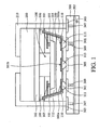
- Fig. 1 is a cross section of an electronic assembly for an image sensor device known to the inventors.
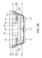
- Figs. 2A to 2E are cross sections of an exemplary embodiment of an electronic assembly for an image sensor device.
- Fig. 1 demonstrates an electronic assembly for an image sensor device known to the inventors. This is not prior art for the purposes of determining the patentability of the invention. This merely shows a problem founded by the inventors.
- the electronic assembly comprises an image sensor chip scale package (CSP) module and a lens set 200 sequentially mounted on a printed circuit board (PCB) 300.
- the CSP module comprises a device chip 104, such as such as a charge-coupled device (CCD) image sensor chip or CMOS image sensor chip, is interposed between lower and upper substrates 100 and 102 comprising glass, quartz or other transparent material.
- the device chip 104 is adhered to the lower substrate 100 via an epoxy layer 112 and is adhered to the upper substrate 102 via a spacer (or dam) 106 forming a cavity 108 therebetween.
- a micro-lens array (not shown) may be formed on the device chip 104 in the cavity 108.
- a conductive layer 101 is disposed along the sidewall and the bottom of the lower substrate 100.
- the conductive layer 101 on the bottom of the lower substrate 100 is patterned to form grounding pads of the CSP module and signal pads. In order to simplify the diagram, only two grounding pads 101a of the CSP module and one signal pad 101b are depicted.
- the conductive layer 101 over the sidewall of the lower substrate 100 laterally contact grounding pads 103 of the device chip 104 to electrically connect the grounding pads 101a of the CSP module and grounding pads 103 of the device chip 104.
- a protective layer 110 covers the conductive layer 101.
- the protective layer 110 at the bottom of the lower substrate 100 is patterned to expose the pads 101a and 101b.
- Solder balls 111 and 113 are respectively disposed on the corresponding pads 101a and 101 b.
- a lens set 200 comprising a stack of multiple lenses (not shown) is mounted on the CSP module to form a compact camera module (CCM).
- the CCM is mounted on the PCB 300 via solder balls 111 and 113.
- the solder balls 111 are electrically connected to a grounding layer 302 inside the PCB 300 through grounding pads 301 of the PCB 300 and plugs 309 thereunder.
- the solder ball 113 is electrically connected to the circuits (not shown) on the PCB 300 through a pad 305.
- a metal housing 210 covers the CCM and is electrically connected to the grounding layer 302 through grounding pads 303 of the PCB 300 and plugs 307 thereunder.
- the metal housing 210 for EMI shielding increase the total volume of the CCM, thus, reducing the size and weight of the CCM is difficult.
- the metal housing for EMI shielding increases manufacturing cost. The inventors have discovered that the following method for fabricating an electronic assembly for an image sensor device can integrate the semiconductor technology with EMI shielding technology without requiring use of a metal housing.
- Fig. 2E illustrates an embodiment of an electronic assembly for an image sensor. Elements in Fig. 2E that are the same as those in Fig. 1 are labeled with the same reference numbers as in Fig. 1 and are not described again for brevity.
- the electronic assembly for the image sensor device comprises a CCM mounted on a PCB 300, comprising a lens set 200, a package module and an opaque conductive layer 220. Similar to the package module shown in Fig.
- the grounding pad 103 of the device chip 104 is electrically connected to the grounding layer 302 inside the PCB 300 through the conductive layer 101, the pad 101a, the solder ball 111, the grounding pad 301 of the PCB 300 and the plug 309 formed in the PCB 300.
- the package module shown in Fig. 2E further comprises a conductive layer 117 similar to the conductive layer 101 on a sidewall 100b of the lower substrate 100, overlying a sidewall 100a of the lower substrate 100, but is insulated from the device chip 104.
- the conductive layer 117 is not connected to any part of grounding pad 103 of the device chip 104 or other input/output pad 119 of the device chip 104, such that the conductive layer 117 is insulated from the devices or circuits (not shown) of the device chip 104.
- the conductive layers 101 and 117 and the pads 111, 113 and 115 comprise a single layer, respectively.
- the conductive layers 101 and 117 and the pads 111, 113 and 115 may comprise a multi-layer structure.
- the multi-layer structure may comprise a plurality layers and a plurality of plugs disposed therebetween for electrical connection.
- the conductive layer 117 extends to the bottom of the lower substrate 100 to form a pad 117a for electrically connecting to the grounding layer 302 through a solder ball 115 formed on the pad 117a and a grounding pad 321 of the PCB 300 and a plug 323 formed in the PCB 300.
- a protective layer 130a covers the conductive layer 117 and exposes a portion of the conductive layer 117 over the sidewall 100a of the lower substrate 100.
- the opaque conductive layer 220 is disposed on the sidewall of the lens set 200 and is electrically connected to the conductive layer 117.
- the opaque conductive layer 220 may, for example, extend onto the package module to directly contact the exposed portion of the conductive layer 117 over the sidewall 100a of the lower substrate 100.
- the opaque conductive layer 220 may comprise metal or other suitable EMI shielding materials. Additionally, because the conductive layer 220 is opaque it may serve as a light-shielding layer.
- Figs. 2A to 2E are cross sections of an exemplary embodiment of an electronic assembly for an image sensor device. Elements in Figs. 2A to 2E that are the same as those in Fig. 1 are labeled with the same reference numbers as Fig. 1 and are not described again for brevity.
- a package module is provided.
- the package module may be fabricated by CSP, wafer level CSP or other conventional package technology. In this embodiment, the package module is preferably fabricated by CSP.
- the package module is similar to that shown in Fig. 1 , with the arrangement of a conductive layer 117 covered by a protective layer 130 being the difference.
- the conductive layer 117 over a sidewall 100a of the lower substrate 100 is insulated from the device chip 104. That is, the conductive layer 117 is not connected to a grounding pad 103 of the device chip 104 or other input/output pad 119 of the device chip 104, such that the conductive layer 117 is insulated from the devices or circuits (not shown) of the device chip 104. Moreover, the conductive layer 117 partially extends to the bottom surface of the lower substrate 100 to serve as a pad 117a. A solder ball 115 is disposed on the pad 117a for a subsequent mounting process.
- the protective layer 130 is partially removed by conventional lithography and etching, to leave a portion of the protective layer 130a, thus, a portion of the protective layer 117 over the sidewall 100a of the lower substrate 100 is exposed.
- the protective layer 130 may be partially removed to expose the portion of the protective layer 117 over the sidewall 100a of the lower substrate 100 prior to formation of solder balls 111, 113 and 115.
- a lens set 200 is subsequently mounted on the package module, as shown in Fig. 2C .
- the lens set comprising a stack of multiple lenses (not shown) does not use a housing or holder for mounting the lens set to the package module.
- an opaque conductive layer 220 is deposited on the sidewall of the lens set 200 and the sidewall of the package module to directly contact the exposed conductive layer 117 over the sidewall 100a of the lower substrate 100.
- the opaque conductive layer 220 may comprise metal or other EMI shielding materials and serve as a light shielding layer.
- the CCM is electrically connected to a PCB 300.
- the CCM is mounted on a PCB 300 through the solder balls 111, 113 and 115 formed on the CCM and the pads 301, 305 and 321 on the PCB 300 for the electrical connection.
- the pad 301 is electrically connected to a grounding layer 302 inside the PCB 300 through a plug 309 for grounding the system.
- the pad 321 is electrically connected to the grounding layer 302 through a plug 323 for EMI shielding.
- the opaque conductive layer 220, the conductive layer 117, the pad 117a and the solder ball 115 can be utilized, rather than the metal housing 210 shown in Fig. 1 , the size and weight of the CCM can be reduced. Moreover, since the electronic assembly for an image sensor device can be fabricated without forming an additional housing or cover for EMI shielding, the manufacturing cost can be reduced.
Landscapes
- Engineering & Computer Science (AREA)
- Multimedia (AREA)
- Signal Processing (AREA)
- Solid State Image Pick-Up Elements (AREA)
- Transforming Light Signals Into Electric Signals (AREA)
- Studio Devices (AREA)
Applications Claiming Priority (2)
| Application Number | Priority Date | Filing Date | Title |
|---|---|---|---|
| US88388907P | 2007-01-08 | 2007-01-08 | |
| US11/707,110 US7679167B2 (en) | 2007-01-08 | 2007-02-16 | Electronic assembly for image sensor device and fabrication method thereof |
Publications (3)
| Publication Number | Publication Date |
|---|---|
| EP1942661A2 true EP1942661A2 (de) | 2008-07-09 |
| EP1942661A3 EP1942661A3 (de) | 2010-11-17 |
| EP1942661B1 EP1942661B1 (de) | 2014-09-17 |
Family
ID=39322768
Family Applications (1)
| Application Number | Title | Priority Date | Filing Date |
|---|---|---|---|
| EP07012091.0A Active EP1942661B1 (de) | 2007-01-08 | 2007-06-20 | Elektronische Anordnung umfassend einen Bildsensorchip und Herstellungsverfahren dafür |
Country Status (5)
| Country | Link |
|---|---|
| US (1) | US7679167B2 (de) |
| EP (1) | EP1942661B1 (de) |
| JP (1) | JP4852675B2 (de) |
| KR (1) | KR100903824B1 (de) |
| TW (1) | TWI334307B (de) |
Cited By (3)
| Publication number | Priority date | Publication date | Assignee | Title |
|---|---|---|---|---|
| EP2282343A1 (de) * | 2009-07-29 | 2011-02-09 | Kingpak Technology Inc. | Bildsensorpaketstruktur |
| US9099368B2 (en) | 2009-11-30 | 2015-08-04 | Stmicroelectronics (Research & Development) Limited | Electromagnetic shielding for camera modules |
| EP2955910A1 (de) * | 2014-06-09 | 2015-12-16 | LG Innotek Co., Ltd. | Kameramodul und fahrzeugkomponente damit |
Families Citing this family (36)
| Publication number | Priority date | Publication date | Assignee | Title |
|---|---|---|---|---|
| KR20070096303A (ko) * | 2006-03-23 | 2007-10-02 | 엘지이노텍 주식회사 | 카메라 모듈용 인쇄회로기판 및 그 제조 방법 |
| US7569409B2 (en) * | 2007-01-04 | 2009-08-04 | Visera Technologies Company Limited | Isolation structures for CMOS image sensor chip scale packages |
| CN101277581B (zh) * | 2007-03-29 | 2011-02-02 | 鸿富锦精密工业(深圳)有限公司 | 电路板的电磁防护方法及电路板组件 |
| DE102007030284B4 (de) * | 2007-06-29 | 2009-12-31 | Schott Ag | Verfahren zum Verpacken von Halbleiter-Bauelementen und verfahrensgemäß hergestelltes Zwischenprodukt |
| US20090026562A1 (en) * | 2007-07-26 | 2009-01-29 | Visera Technologies Company Limited | Package structure for optoelectronic device |
| KR100959922B1 (ko) * | 2007-11-20 | 2010-05-26 | 삼성전자주식회사 | 카메라 모듈 및 그 제조방법 |
| US7829966B2 (en) * | 2007-11-23 | 2010-11-09 | Visera Technologies Company Limited | Electronic assembly for image sensor device |
| KR20090108233A (ko) * | 2008-04-11 | 2009-10-15 | 삼성전자주식회사 | 카메라 모듈의 제조 방법, 이에 의해 제작된 카메라 모듈및 상기 카메라 모듈을 포함하는 전자 시스템 |
| US7964936B2 (en) * | 2008-07-10 | 2011-06-21 | Visera Technologies Company Limited | Electronic device package with electromagnetic compatibility (EMC) coating thereon |
| KR100982270B1 (ko) * | 2008-08-08 | 2010-09-15 | 삼성전기주식회사 | 카메라 모듈 및 이의 제조 방법 |
| JP5498684B2 (ja) | 2008-11-07 | 2014-05-21 | ラピスセミコンダクタ株式会社 | 半導体モジュール及びその製造方法 |
| US8351219B2 (en) * | 2009-09-03 | 2013-01-08 | Visera Technologies Company Limited | Electronic assembly for an image sensing device |
| KR20110064156A (ko) * | 2009-12-07 | 2011-06-15 | 삼성전자주식회사 | 촬상 장치 및 그 제조방법 |
| US9330892B2 (en) * | 2009-12-31 | 2016-05-03 | Spectro Analytical Instruments Gmbh | Simultaneous inorganic mass spectrometer and method of inorganic mass spectrometry |
| JP5682185B2 (ja) * | 2010-09-07 | 2015-03-11 | ソニー株式会社 | 半導体パッケージおよび半導体パッケージの製造方法ならびに光学モジュール |
| JP2013012615A (ja) * | 2011-06-29 | 2013-01-17 | Fujifilm Corp | 固体撮像素子及びその製造方法、それに用いる固体撮像素子用の透明導電性膜 |
| CA2878514A1 (en) | 2012-07-26 | 2014-01-30 | Olive Medical Corporation | Ycbcr pulsed illumination scheme in a light deficient environment |
| WO2014018936A2 (en) | 2012-07-26 | 2014-01-30 | Olive Medical Corporation | Continuous video in a light deficient environment |
| JP6034725B2 (ja) * | 2013-03-05 | 2016-11-30 | 太陽誘電株式会社 | カメラモジュール |
| US9777913B2 (en) | 2013-03-15 | 2017-10-03 | DePuy Synthes Products, Inc. | Controlling the integral light energy of a laser pulse |
| CA2906798A1 (en) | 2013-03-15 | 2014-09-18 | Olive Medical Corporation | Super resolution and color motion artifact correction in a pulsed color imaging system |
| EP2967301B1 (de) | 2013-03-15 | 2021-11-03 | DePuy Synthes Products, Inc. | Bereichsmessung in einer lichtkontrollierten umgebung |
| US9231124B2 (en) * | 2013-09-25 | 2016-01-05 | Delphi Technologies, Inc. | Ball grid array packaged camera device soldered to a substrate |
| EP3119265B1 (de) * | 2014-03-21 | 2019-09-11 | DePuy Synthes Products, Inc. | Kartenrandstecker für abbildungssensoren |
| US9704772B2 (en) | 2014-04-02 | 2017-07-11 | Xintec Inc. | Chip package and method for forming the same |
| CN104201115A (zh) * | 2014-09-12 | 2014-12-10 | 苏州晶方半导体科技股份有限公司 | 晶圆级指纹识别芯片封装结构及封装方法 |
| TWI588954B (zh) * | 2015-02-16 | 2017-06-21 | 精材科技股份有限公司 | 晶片封裝體及其製造方法 |
| US20170186712A1 (en) * | 2015-12-29 | 2017-06-29 | Xintec Inc. | Chip package and method for forming the same |
| US9769398B2 (en) | 2016-01-06 | 2017-09-19 | Microsoft Technology Licensing, Llc | Image sensor with large-area global shutter contact |
| US20190148429A1 (en) | 2016-03-12 | 2019-05-16 | Ningbo Sunny Opotech Co., Ltd. | Camera module, and photosensitive component thereof and manufacturing method therefor |
| US10325952B2 (en) * | 2017-07-07 | 2019-06-18 | Advanced Semiconductor Engineering, Inc. | Semiconductor package device and method of manufacturing the same |
| US10868061B2 (en) * | 2018-08-13 | 2020-12-15 | Semiconductor Components Industries, Llc | Packaging structure for a sensor having a sealing layer |
| US11276724B2 (en) * | 2019-06-27 | 2022-03-15 | Semiconductor Components Industries, Llc | Electrical interconnection of image sensor package |
| US11206732B2 (en) * | 2019-07-02 | 2021-12-21 | Waymo Llc | Reliable interconnect for camera image sensors |
| CN112187970B (zh) * | 2019-07-05 | 2022-05-27 | 三赢科技(深圳)有限公司 | 摄像头模组及其电子装置 |
| US11063083B2 (en) * | 2019-10-11 | 2021-07-13 | Omnivision Technologies, Inc. | Light-shielded cameras and methods of manufacture |
Family Cites Families (15)
| Publication number | Priority date | Publication date | Assignee | Title |
|---|---|---|---|---|
| US5400072A (en) * | 1988-12-23 | 1995-03-21 | Hitachi, Ltd. | Video camera unit having an airtight mounting arrangement for an image sensor chip |
| IL133453A0 (en) * | 1999-12-10 | 2001-04-30 | Shellcase Ltd | Methods for producing packaged integrated circuit devices and packaged integrated circuit devices produced thereby |
| WO2001091193A2 (en) * | 2000-05-23 | 2001-11-29 | Atmel Corporation | Integrated ic chip package for electronic image sensor die |
| JP3839271B2 (ja) * | 2001-05-01 | 2006-11-01 | 富士写真フイルム株式会社 | 固体撮像装置及びその製造方法 |
| JP2004119917A (ja) * | 2002-09-30 | 2004-04-15 | Sanyo Electric Co Ltd | 半導体装置及びその製造方法 |
| JP2005086100A (ja) * | 2003-09-10 | 2005-03-31 | Fuji Photo Film Co Ltd | 固体撮像装置 |
| JP4753170B2 (ja) * | 2004-03-05 | 2011-08-24 | 三洋電機株式会社 | 半導体装置及びその製造方法 |
| JP2005348275A (ja) * | 2004-06-04 | 2005-12-15 | Sharp Corp | 撮像素子およびカメラモジュール |
| KR100629467B1 (ko) * | 2004-07-14 | 2006-09-27 | (주) 윈팩 | 이미지 센서용 패키지 |
| JP4139803B2 (ja) * | 2004-09-28 | 2008-08-27 | シャープ株式会社 | 半導体装置の製造方法 |
| KR100608420B1 (ko) * | 2004-11-01 | 2006-08-02 | 동부일렉트로닉스 주식회사 | 이미지 센서 칩 패키지 및 그 제조방법 |
| KR20060106891A (ko) * | 2005-04-04 | 2006-10-12 | 마츠시타 덴끼 산교 가부시키가이샤 | 광학 디바이스용 캐비티 구조체, 광학 디바이스 및 광학디바이스용 캐비티 구조체의 제조방법 |
| US20070052827A1 (en) * | 2005-09-07 | 2007-03-08 | Omnivision Technologies, Inc. | Coated wafer level camera modules and associated methods |
| JP2007165696A (ja) * | 2005-12-15 | 2007-06-28 | Sanyo Electric Co Ltd | 半導体装置及びその製造方法 |
| US7663213B2 (en) * | 2006-11-13 | 2010-02-16 | China Wafer Level Csp Ltd. | Wafer level chip size packaged chip device with a double-layer lead structure and method of fabricating the same |
-
2007
- 2007-02-16 US US11/707,110 patent/US7679167B2/en active Active
- 2007-06-20 TW TW096122117A patent/TWI334307B/zh active
- 2007-06-20 EP EP07012091.0A patent/EP1942661B1/de active Active
- 2007-07-10 KR KR1020070068980A patent/KR100903824B1/ko active Active
- 2007-09-05 JP JP2007230285A patent/JP4852675B2/ja active Active
Cited By (4)
| Publication number | Priority date | Publication date | Assignee | Title |
|---|---|---|---|---|
| EP2282343A1 (de) * | 2009-07-29 | 2011-02-09 | Kingpak Technology Inc. | Bildsensorpaketstruktur |
| US9099368B2 (en) | 2009-11-30 | 2015-08-04 | Stmicroelectronics (Research & Development) Limited | Electromagnetic shielding for camera modules |
| EP2955910A1 (de) * | 2014-06-09 | 2015-12-16 | LG Innotek Co., Ltd. | Kameramodul und fahrzeugkomponente damit |
| KR20150140927A (ko) * | 2014-06-09 | 2015-12-17 | 엘지이노텍 주식회사 | 카메라 모듈 및 이를 포함하는 차량 부품 |
Also Published As
| Publication number | Publication date |
|---|---|
| TW200830870A (en) | 2008-07-16 |
| JP2008172191A (ja) | 2008-07-24 |
| US7679167B2 (en) | 2010-03-16 |
| KR100903824B1 (ko) | 2009-06-25 |
| JP4852675B2 (ja) | 2012-01-11 |
| EP1942661B1 (de) | 2014-09-17 |
| TWI334307B (en) | 2010-12-01 |
| US20080164550A1 (en) | 2008-07-10 |
| KR20080065221A (ko) | 2008-07-11 |
| EP1942661A3 (de) | 2010-11-17 |
Similar Documents
| Publication | Publication Date | Title |
|---|---|---|
| US7679167B2 (en) | Electronic assembly for image sensor device and fabrication method thereof | |
| US7829966B2 (en) | Electronic assembly for image sensor device | |
| US8351219B2 (en) | Electronic assembly for an image sensing device | |
| US7019374B2 (en) | Small-sized image pick up module | |
| US7361989B1 (en) | Stacked imager package | |
| CN103066061B (zh) | 相机模块及包括相机模块的系统 | |
| KR101070058B1 (ko) | 카메라 모듈 패키지 | |
| US20090256931A1 (en) | Camera module, method of manufacturing the same, and electronic system having the same | |
| KR20080053202A (ko) | 이미지 센서 모듈 | |
| US20050270405A1 (en) | Image pickup device and camera module | |
| CN100544011C (zh) | 图像传感装置及其制造方法 | |
| CN103081105B (zh) | 图像拾取装置、图像拾取模块和照相机 | |
| KR20080079086A (ko) | 이미지 센서 모듈과 이를 구비한 카메라 모듈 및 그 제조방법 | |
| US20060289733A1 (en) | Stack-type image sensor module | |
| US8835992B2 (en) | Electronic device comprising electrical contact pads | |
| US20140110713A1 (en) | Electronic device and method of fabricating the same | |
| KR20060007848A (ko) | 이미지 센서 모듈 | |
| HK1181919A (en) | Camera module and system comprising the same | |
| HK1181919B (en) | Camera module and system comprising the same |
Legal Events
| Date | Code | Title | Description |
|---|---|---|---|
| PUAI | Public reference made under article 153(3) epc to a published international application that has entered the european phase |
Free format text: ORIGINAL CODE: 0009012 |
|
| AK | Designated contracting states |
Kind code of ref document: A2 Designated state(s): AT BE BG CH CY CZ DE DK EE ES FI FR GB GR HU IE IS IT LI LT LU LV MC MT NL PL PT RO SE SI SK TR |
|
| AX | Request for extension of the european patent |
Extension state: AL BA HR MK RS |
|
| 17P | Request for examination filed |
Effective date: 20081002 |
|
| PUAL | Search report despatched |
Free format text: ORIGINAL CODE: 0009013 |
|
| AK | Designated contracting states |
Kind code of ref document: A3 Designated state(s): AT BE BG CH CY CZ DE DK EE ES FI FR GB GR HU IE IS IT LI LT LU LV MC MT NL PL PT RO SE SI SK TR |
|
| AX | Request for extension of the european patent |
Extension state: AL BA HR MK RS |
|
| AKX | Designation fees paid |
Designated state(s): AT BE BG CH CY CZ DE DK EE ES FI FR GB GR HU IE IS IT LI LT LU LV MC MT NL PL PT RO SE SI SK TR |
|
| RAP1 | Party data changed (applicant data changed or rights of an application transferred) |
Owner name: VISERA TECHNOLOGIES COMPANY LIMITED Owner name: OMNIVISION TECHNOLOGIES, INC. |
|
| 17Q | First examination report despatched |
Effective date: 20140214 |
|
| GRAP | Despatch of communication of intention to grant a patent |
Free format text: ORIGINAL CODE: EPIDOSNIGR1 |
|
| INTG | Intention to grant announced |
Effective date: 20140620 |
|
| GRAS | Grant fee paid |
Free format text: ORIGINAL CODE: EPIDOSNIGR3 |
|
| GRAA | (expected) grant |
Free format text: ORIGINAL CODE: 0009210 |
|
| RAP1 | Party data changed (applicant data changed or rights of an application transferred) |
Owner name: OMNIVISION TECHNOLOGIES, INC. Owner name: VISERA TECHNOLOGIES COMPANY LIMITED |
|
| AK | Designated contracting states |
Kind code of ref document: B1 Designated state(s): AT BE BG CH CY CZ DE DK EE ES FI FR GB GR HU IE IS IT LI LT LU LV MC MT NL PL PT RO SE SI SK TR |
|
| REG | Reference to a national code |
Ref country code: GB Ref legal event code: FG4D |
|
| REG | Reference to a national code |
Ref country code: CH Ref legal event code: NV Representative=s name: ROTTMANN, ZIMMERMANN + PARTNER AG, CH Ref country code: CH Ref legal event code: EP |
|
| REG | Reference to a national code |
Ref country code: IE Ref legal event code: FG4D |
|
| REG | Reference to a national code |
Ref country code: AT Ref legal event code: REF Ref document number: 688143 Country of ref document: AT Kind code of ref document: T Effective date: 20141015 |
|
| REG | Reference to a national code |
Ref country code: DE Ref legal event code: R096 Ref document number: 602007038554 Country of ref document: DE Effective date: 20141030 |
|
| REG | Reference to a national code |
Ref country code: NL Ref legal event code: T3 |
|
| PG25 | Lapsed in a contracting state [announced via postgrant information from national office to epo] |
Ref country code: GR Free format text: LAPSE BECAUSE OF FAILURE TO SUBMIT A TRANSLATION OF THE DESCRIPTION OR TO PAY THE FEE WITHIN THE PRESCRIBED TIME-LIMIT Effective date: 20141218 Ref country code: FI Free format text: LAPSE BECAUSE OF FAILURE TO SUBMIT A TRANSLATION OF THE DESCRIPTION OR TO PAY THE FEE WITHIN THE PRESCRIBED TIME-LIMIT Effective date: 20140917 Ref country code: LT Free format text: LAPSE BECAUSE OF FAILURE TO SUBMIT A TRANSLATION OF THE DESCRIPTION OR TO PAY THE FEE WITHIN THE PRESCRIBED TIME-LIMIT Effective date: 20140917 Ref country code: SE Free format text: LAPSE BECAUSE OF FAILURE TO SUBMIT A TRANSLATION OF THE DESCRIPTION OR TO PAY THE FEE WITHIN THE PRESCRIBED TIME-LIMIT Effective date: 20140917 |
|
| REG | Reference to a national code |
Ref country code: LT Ref legal event code: MG4D |
|
| PG25 | Lapsed in a contracting state [announced via postgrant information from national office to epo] |
Ref country code: CY Free format text: LAPSE BECAUSE OF FAILURE TO SUBMIT A TRANSLATION OF THE DESCRIPTION OR TO PAY THE FEE WITHIN THE PRESCRIBED TIME-LIMIT Effective date: 20140917 Ref country code: LV Free format text: LAPSE BECAUSE OF FAILURE TO SUBMIT A TRANSLATION OF THE DESCRIPTION OR TO PAY THE FEE WITHIN THE PRESCRIBED TIME-LIMIT Effective date: 20140917 |
|
| REG | Reference to a national code |
Ref country code: AT Ref legal event code: MK05 Ref document number: 688143 Country of ref document: AT Kind code of ref document: T Effective date: 20140917 |
|
| PG25 | Lapsed in a contracting state [announced via postgrant information from national office to epo] |
Ref country code: ES Free format text: LAPSE BECAUSE OF FAILURE TO SUBMIT A TRANSLATION OF THE DESCRIPTION OR TO PAY THE FEE WITHIN THE PRESCRIBED TIME-LIMIT Effective date: 20140917 Ref country code: CZ Free format text: LAPSE BECAUSE OF FAILURE TO SUBMIT A TRANSLATION OF THE DESCRIPTION OR TO PAY THE FEE WITHIN THE PRESCRIBED TIME-LIMIT Effective date: 20140917 Ref country code: RO Free format text: LAPSE BECAUSE OF FAILURE TO SUBMIT A TRANSLATION OF THE DESCRIPTION OR TO PAY THE FEE WITHIN THE PRESCRIBED TIME-LIMIT Effective date: 20140917 Ref country code: PT Free format text: LAPSE BECAUSE OF FAILURE TO SUBMIT A TRANSLATION OF THE DESCRIPTION OR TO PAY THE FEE WITHIN THE PRESCRIBED TIME-LIMIT Effective date: 20150119 Ref country code: EE Free format text: LAPSE BECAUSE OF FAILURE TO SUBMIT A TRANSLATION OF THE DESCRIPTION OR TO PAY THE FEE WITHIN THE PRESCRIBED TIME-LIMIT Effective date: 20140917 Ref country code: IS Free format text: LAPSE BECAUSE OF FAILURE TO SUBMIT A TRANSLATION OF THE DESCRIPTION OR TO PAY THE FEE WITHIN THE PRESCRIBED TIME-LIMIT Effective date: 20150117 Ref country code: SK Free format text: LAPSE BECAUSE OF FAILURE TO SUBMIT A TRANSLATION OF THE DESCRIPTION OR TO PAY THE FEE WITHIN THE PRESCRIBED TIME-LIMIT Effective date: 20140917 |
|
| PG25 | Lapsed in a contracting state [announced via postgrant information from national office to epo] |
Ref country code: AT Free format text: LAPSE BECAUSE OF FAILURE TO SUBMIT A TRANSLATION OF THE DESCRIPTION OR TO PAY THE FEE WITHIN THE PRESCRIBED TIME-LIMIT Effective date: 20140917 Ref country code: PL Free format text: LAPSE BECAUSE OF FAILURE TO SUBMIT A TRANSLATION OF THE DESCRIPTION OR TO PAY THE FEE WITHIN THE PRESCRIBED TIME-LIMIT Effective date: 20140917 |
|
| REG | Reference to a national code |
Ref country code: DE Ref legal event code: R097 Ref document number: 602007038554 Country of ref document: DE |
|
| PLBE | No opposition filed within time limit |
Free format text: ORIGINAL CODE: 0009261 |
|
| STAA | Information on the status of an ep patent application or granted ep patent |
Free format text: STATUS: NO OPPOSITION FILED WITHIN TIME LIMIT |
|
| PG25 | Lapsed in a contracting state [announced via postgrant information from national office to epo] |
Ref country code: DK Free format text: LAPSE BECAUSE OF FAILURE TO SUBMIT A TRANSLATION OF THE DESCRIPTION OR TO PAY THE FEE WITHIN THE PRESCRIBED TIME-LIMIT Effective date: 20140917 |
|
| 26N | No opposition filed |
Effective date: 20150618 |
|
| PG25 | Lapsed in a contracting state [announced via postgrant information from national office to epo] |
Ref country code: IT Free format text: LAPSE BECAUSE OF FAILURE TO SUBMIT A TRANSLATION OF THE DESCRIPTION OR TO PAY THE FEE WITHIN THE PRESCRIBED TIME-LIMIT Effective date: 20140917 |
|
| PG25 | Lapsed in a contracting state [announced via postgrant information from national office to epo] |
Ref country code: SI Free format text: LAPSE BECAUSE OF FAILURE TO SUBMIT A TRANSLATION OF THE DESCRIPTION OR TO PAY THE FEE WITHIN THE PRESCRIBED TIME-LIMIT Effective date: 20140917 |
|
| PG25 | Lapsed in a contracting state [announced via postgrant information from national office to epo] |
Ref country code: MC Free format text: LAPSE BECAUSE OF FAILURE TO SUBMIT A TRANSLATION OF THE DESCRIPTION OR TO PAY THE FEE WITHIN THE PRESCRIBED TIME-LIMIT Effective date: 20140917 |
|
| PG25 | Lapsed in a contracting state [announced via postgrant information from national office to epo] |
Ref country code: LU Free format text: LAPSE BECAUSE OF FAILURE TO SUBMIT A TRANSLATION OF THE DESCRIPTION OR TO PAY THE FEE WITHIN THE PRESCRIBED TIME-LIMIT Effective date: 20150620 |
|
| REG | Reference to a national code |
Ref country code: IE Ref legal event code: MM4A |
|
| REG | Reference to a national code |
Ref country code: FR Ref legal event code: PLFP Year of fee payment: 10 |
|
| PG25 | Lapsed in a contracting state [announced via postgrant information from national office to epo] |
Ref country code: IE Free format text: LAPSE BECAUSE OF NON-PAYMENT OF DUE FEES Effective date: 20150620 |
|
| REG | Reference to a national code |
Ref country code: CH Ref legal event code: PCAR Free format text: NEW ADDRESS: GARTENSTRASSE 28 A, 5400 BADEN (CH) |
|
| PG25 | Lapsed in a contracting state [announced via postgrant information from national office to epo] |
Ref country code: MT Free format text: LAPSE BECAUSE OF FAILURE TO SUBMIT A TRANSLATION OF THE DESCRIPTION OR TO PAY THE FEE WITHIN THE PRESCRIBED TIME-LIMIT Effective date: 20140917 |
|
| REG | Reference to a national code |
Ref country code: FR Ref legal event code: PLFP Year of fee payment: 11 |
|
| PG25 | Lapsed in a contracting state [announced via postgrant information from national office to epo] |
Ref country code: BG Free format text: LAPSE BECAUSE OF FAILURE TO SUBMIT A TRANSLATION OF THE DESCRIPTION OR TO PAY THE FEE WITHIN THE PRESCRIBED TIME-LIMIT Effective date: 20140917 Ref country code: HU Free format text: LAPSE BECAUSE OF FAILURE TO SUBMIT A TRANSLATION OF THE DESCRIPTION OR TO PAY THE FEE WITHIN THE PRESCRIBED TIME-LIMIT; INVALID AB INITIO Effective date: 20070620 |
|
| PG25 | Lapsed in a contracting state [announced via postgrant information from national office to epo] |
Ref country code: TR Free format text: LAPSE BECAUSE OF FAILURE TO SUBMIT A TRANSLATION OF THE DESCRIPTION OR TO PAY THE FEE WITHIN THE PRESCRIBED TIME-LIMIT Effective date: 20140917 |
|
| PG25 | Lapsed in a contracting state [announced via postgrant information from national office to epo] |
Ref country code: BE Free format text: LAPSE BECAUSE OF FAILURE TO SUBMIT A TRANSLATION OF THE DESCRIPTION OR TO PAY THE FEE WITHIN THE PRESCRIBED TIME-LIMIT Effective date: 20140917 |
|
| REG | Reference to a national code |
Ref country code: FR Ref legal event code: PLFP Year of fee payment: 12 |
|
| REG | Reference to a national code |
Ref country code: DE Ref legal event code: R081 Ref document number: 602007038554 Country of ref document: DE Owner name: VISERA TECHNOLOGIES COMPANY LTD., TW Free format text: FORMER OWNER: OMNIVISION TECHNOLOGIES, INC., SANTA CLARA, CALIF., US Ref country code: DE Ref legal event code: R081 Ref document number: 602007038554 Country of ref document: DE Owner name: OMNIVISION TECHNOLOGIES, INC., SANTA CLARA, US Free format text: FORMER OWNER: OMNIVISION TECHNOLOGIES, INC., SANTA CLARA, CALIF., US Ref country code: DE Ref legal event code: R082 Ref document number: 602007038554 Country of ref document: DE Representative=s name: TER MEER STEINMEISTER & PARTNER PATENTANWAELTE, DE |
|
| REG | Reference to a national code |
Ref country code: DE Ref legal event code: R079 Ref document number: 602007038554 Country of ref document: DE Free format text: PREVIOUS MAIN CLASS: H04N0005225000 Ipc: H04N0023000000 |
|
| P01 | Opt-out of the competence of the unified patent court (upc) registered |
Effective date: 20230525 |
|
| PGFP | Annual fee paid to national office [announced via postgrant information from national office to epo] |
Ref country code: DE Payment date: 20250627 Year of fee payment: 19 |
|
| PGFP | Annual fee paid to national office [announced via postgrant information from national office to epo] |
Ref country code: GB Payment date: 20250627 Year of fee payment: 19 |
|
| PGFP | Annual fee paid to national office [announced via postgrant information from national office to epo] |
Ref country code: NL Payment date: 20250626 Year of fee payment: 19 |
|
| PGFP | Annual fee paid to national office [announced via postgrant information from national office to epo] |
Ref country code: FR Payment date: 20250625 Year of fee payment: 19 |
|
| PGFP | Annual fee paid to national office [announced via postgrant information from national office to epo] |
Ref country code: CH Payment date: 20250701 Year of fee payment: 19 |
|
| REG | Reference to a national code |
Ref country code: CH Ref legal event code: R17 Free format text: ST27 STATUS EVENT CODE: U-0-0-R10-R17 (AS PROVIDED BY THE NATIONAL OFFICE) Effective date: 20260410 |