EP2955910A1 - Kameramodul und fahrzeugkomponente damit - Google Patents
Kameramodul und fahrzeugkomponente damit Download PDFInfo
- Publication number
- EP2955910A1 EP2955910A1 EP15167867.9A EP15167867A EP2955910A1 EP 2955910 A1 EP2955910 A1 EP 2955910A1 EP 15167867 A EP15167867 A EP 15167867A EP 2955910 A1 EP2955910 A1 EP 2955910A1
- Authority
- EP
- European Patent Office
- Prior art keywords
- circuit board
- camera module
- connector
- connection portion
- module according
- Prior art date
- Legal status (The legal status is an assumption and is not a legal conclusion. Google has not performed a legal analysis and makes no representation as to the accuracy of the status listed.)
- Granted
Links
Images



Classifications
-
- B—PERFORMING OPERATIONS; TRANSPORTING
- B60—VEHICLES IN GENERAL
- B60R—VEHICLES, VEHICLE FITTINGS, OR VEHICLE PARTS, NOT OTHERWISE PROVIDED FOR
- B60R1/00—Optical viewing arrangements; Real-time viewing arrangements for drivers or passengers using optical image capturing systems, e.g. cameras or video systems specially adapted for use in or on vehicles
- B60R1/20—Real-time viewing arrangements for drivers or passengers using optical image capturing systems, e.g. cameras or video systems specially adapted for use in or on vehicles
- B60R1/22—Real-time viewing arrangements for drivers or passengers using optical image capturing systems, e.g. cameras or video systems specially adapted for use in or on vehicles for viewing an area outside the vehicle, e.g. the exterior of the vehicle
-
- B—PERFORMING OPERATIONS; TRANSPORTING
- B60—VEHICLES IN GENERAL
- B60R—VEHICLES, VEHICLE FITTINGS, OR VEHICLE PARTS, NOT OTHERWISE PROVIDED FOR
- B60R11/00—Arrangements for holding or mounting articles, not otherwise provided for
- B60R11/04—Mounting of cameras operative during drive; Arrangement of controls thereof relative to the vehicle
-
- G—PHYSICS
- G03—PHOTOGRAPHY; CINEMATOGRAPHY; ANALOGOUS TECHNIQUES USING WAVES OTHER THAN OPTICAL WAVES; ELECTROGRAPHY; HOLOGRAPHY
- G03B—APPARATUS OR ARRANGEMENTS FOR TAKING PHOTOGRAPHS OR FOR PROJECTING OR VIEWING THEM; APPARATUS OR ARRANGEMENTS EMPLOYING ANALOGOUS TECHNIQUES USING WAVES OTHER THAN OPTICAL WAVES; ACCESSORIES THEREFOR
- G03B17/00—Details of cameras or camera bodies; Accessories therefor
- G03B17/02—Bodies
-
- H—ELECTRICITY
- H04—ELECTRIC COMMUNICATION TECHNIQUE
- H04N—PICTORIAL COMMUNICATION, e.g. TELEVISION
- H04N23/00—Cameras or camera modules comprising electronic image sensors; Control thereof
- H04N23/50—Constructional details
-
- H—ELECTRICITY
- H04—ELECTRIC COMMUNICATION TECHNIQUE
- H04N—PICTORIAL COMMUNICATION, e.g. TELEVISION
- H04N23/00—Cameras or camera modules comprising electronic image sensors; Control thereof
- H04N23/50—Constructional details
- H04N23/51—Housings
-
- H—ELECTRICITY
- H04—ELECTRIC COMMUNICATION TECHNIQUE
- H04N—PICTORIAL COMMUNICATION, e.g. TELEVISION
- H04N23/00—Cameras or camera modules comprising electronic image sensors; Control thereof
- H04N23/50—Constructional details
- H04N23/54—Mounting of pick-up tubes, electronic image sensors, deviation or focusing coils
-
- H—ELECTRICITY
- H04—ELECTRIC COMMUNICATION TECHNIQUE
- H04N—PICTORIAL COMMUNICATION, e.g. TELEVISION
- H04N23/00—Cameras or camera modules comprising electronic image sensors; Control thereof
- H04N23/57—Mechanical or electrical details of cameras or camera modules specially adapted for being embedded in other devices
Definitions
- Embodiments relate to a camera module and a vehicle component including the same.
- a camera module is a sort of an image capture device that captures an image and converts the captured image into an electrical signal.
- the camera module may be applied to various fields including, for example, vehicles or crime prevention.
- the camera module may be used to capture an image of the periphery of a vehicle to assist safe traveling of a driver.
- a Printed Circuit Board (PCB) incorporated in the module is affected by the ESD, which may cause various Integrated Circuits (ICs) mounted on the PCB to malfunction due to noise.
- ICs Integrated Circuits
- the camera module may suffer from deterioration in resolution or operational errors such as, for example, screen darkening or screen overlap, which makes it impossible for the camera module to correctly function.
- the present embodiment provides a camera module and a vehicle component including the same to solve problems of the related art.
- Embodiments provide a camera module having a circuit board that is not affected by electrostatic discharge and a vehicle component including the same.
- a camera module in one embodiment, includes a housing and a circuit board accommodated in the housing, the circuit board being connectable to a connector including a metal, wherein the circuit board includes a ground portion and a connection portion located to be electrically insulated from the ground portion, the connection portion being connectable to the connector.
- the ground portion may be a body of the circuit board or a portion of the body.
- the metal may correspond to a support member configured to maintain a shape of the connector.
- the connector may include a flexible material.
- the ground portion and the connection portion may be disconnected from each other.
- the circuit board may further include an electrically insulating member disposed between the ground portion and the connection portion.
- connection portion may include a power input terminal connected to the connector to supply power to the circuit board.
- connection portion may include a signal input and output terminal connected to the connector to supply a signal to the circuit board or to receive a signal from the circuit board.
- the circuit board may include at least one functional element, and the at least one functional element may be connected to the ground portion of the circuit board.
- the camera module may further include a lens
- the at least one functional element may include at least one of an image sensor configured to convert an optical image from the lens into an electrical image signal, an oscillator configured to generate a clock signal required for the image sensor, a video amplifier configured to amplify the image signal and output the amplified image signal as a video signal, a converter configured to convert a level of input power to a level of power required for the circuit board, or a controller configured to control at least one of the image sensor or the converter.
- the converter may include at least one of a direct current (DC)-DC converter or a low voltage drop out regulator.
- the at least one functional element may further include a storage unit configured to temporarily store the electrical image signal generated in the image sensor.
- the storage unit may include a flash memory.
- connection portion may receive the input power to provide the converter with the received input power.
- a vehicle camera module in another embodiment, includes a housing and a circuit board accommodated in the housing, the circuit board being connectable to a connector, the connector including a metal and being configured to receive power through a first cable from a battery, wherein the circuit board includes a ground portion and a connection portion disposed to be electrically insulated from the ground portion, the connection portion being connectable to the connector.
- the first cable may have a length of 10 cm or 15 cm or more.
- the connector may transmit a surrounding image generated in the vehicle camera module to an electronic control unit (ECU) through a second cable, the ECU being included in a vehicle to analyze the surrounding image of the vehicle.
- the second cable may have a length of 10 cm or 15 cm or more.
- the surrounding image of the vehicle may include an image of at least one of the front side or the rear side of the vehicle.
- a vehicle component includes the vehicle camera module.
- relative terms such as, for example, “first”, “second”, “on/upper/above” and “beneath/lower/below”, used in the following description may be used to distinguish any one substance or element with another substance or element without requiring or containing any physical or logical relationship or sequence between these substances or elements.
- FIG. 1 is a view illustrating a camera module 100 according to an embodiment.
- the camera module 100 illustrated in FIG. 1 may include a housing (or case) 110 and a circuit board 120.
- the housing 110 may serve to accommodate the circuit board 120 therein. That is, the housing 110 may serve as a protective shield to protect internal components of the camera module 100, for example, the circuit board 120 from, for example, outside dust or moisture.
- the housing 110 may be formed of, for example, plastic, polypropylene (PP), polyethylene (PE), or polycarbonate (PC) and may be wholly or partially formed of a metal.
- polycarbonate has excellent light resistance and heat resistance as well as high strength.
- the housing 110 may be formed via blow molding, the embodiment is not limited as to the material or external shape of the housing 110.
- a connector 200 may be electrically connected to the circuit board 120 received in the housing 110.
- the connector 200 may include a frame 210, a metal 220, and a protrusion 230.
- the metal 220 may be affixed to the exterior of the frame 210.
- the metal 220 may serve as a support member.
- the support member 220 may serve to maintain the shape of the frame 210 in an original state so as to prevent deformation of the connector 200.
- a pair of metals 220 serving as support members may be attached to both sides of the frame 210.
- the embodiment is not limited to this attachment form of the metal 220.
- the protrusion 230 may be shaped to protrude from the frame 210 to provide the connector 200 with a shape suitable for coupling to or separation from a connection element 124 of the circuit board 120 in a direction designated by the arrow 30.
- the circuit board 120 may include a ground portion 122 and the connection portion 124.
- the circuit board 120 may mean a Printed Circuit Board (PCB).
- the ground portion 122 is illustrated in a conceptual block in FIG. 1 , and may be a body itself of the circuit board 120 or a portion of the body rather than being separately present.
- connection portion 124 may be shaped to be connectable to the connector 200.
- the connection portion 124 may be shaped to allow the protrusion 230 to be introduced into the connection portion 124.
- connection portion 124 may include N terminals 124-1, ..., 124-N to perform various functions.
- N is a positive integer greater than or equal to 1.
- the N terminals 124-1 to 124-N have take the form of pins to be connectable to the connector 200, the embodiment is not limited to these shapes of the N terminals 124-1 to 124-N.
- the N terminals 124-1 to 124-N may include at least one of a power input terminal or a signal input/output terminal.
- the power input terminal may be connected to the connector 200 and serve to receive power required for the circuit board 120.
- the signal input/output terminal may be connected to the connector 200 and serve to receive a signal transmitted to the circuit board 120 or to transmit a signal from the circuit board 120.
- connection portion 124 may serve as an interface between the connector 200 and the circuit board 120.
- the circuit board 120 may include at least one functional element (or an Integrated Circuit (IC)).
- the at least one functional element may include first to K th functional elements 126-1, 126-2, ..., 126-K.
- K is a positive integer greater than or equal to 1.
- the first to K th functional elements 126-1, 126-2, ..., 126-K may be connected to the ground portion 122 of the circuit board 120.
- the ground portion 122 is a body itself of the circuit board 120 as described above rather than being a separate member
- the first to K th functional elements 126-1, 126-2, ..., 126-K may be in electrical conduction with the circuit board 120. Examples of each of the first to K th functional elements 126-1, 126-2, ..., 126-K will be described later in more detail with reference to FIG. 2 .
- an external device 400 may be connected to the connector 200 through a cable 300 and may function not only to supply a signal or power required for the circuit board 120, but also to analyze and process a signal generated or processed in the circuit board 120.
- the external device 400 may be a power supply.
- the connector 200 may transmit power, supplied from the power supply unit 400 through the cable 300, to the power input terminal of the connection portion 124 of the circuit board 120.
- the external device 400 may be an image signal analyzer.
- the connector 200 may receive an image signal from the circuit board 120 and transmit the image signal to the image signal analyzer 400 through the cable 300.
- the image signal analyzer 400 may analyze an image signal provided from the circuit board 120 of the camera module 100.
- the embodiment is not limited to the above-described examples of the external device 400, and the external device 400 may perform various other functions.
- the camera module 100 may be connected to the external device 400 through the connector 200 and the cable 300.
- connection portion 124 of the circuit board 120 may be disposed to be electrically insulated from the ground portion 122. That is, the connection portion 124 and the ground portion 122 may be electrically floated.
- ground portion 122 and the connection portion 124 may be disconnected from each other, or electrically disconnected.
- the circuit board 120 may further include an electrically insulating member 128.
- the electrically insulating member 128 may be located between the ground portion 122 and the connection portion 124 to electrically insulate the ground portion 122 and the connection portion 124.
- the camera module 100 in accordance with the embodiment includes the housing 110
- electrostatic discharge (ESD) 10 applied from the exterior to the camera module 100 may first reach the housing 110.
- the electrostatic discharge 10 may be introduced into the connection portion 124 of the camera module 100 through the metal 220 of the connector 200.
- connection portion 124 when the connection portion 124 is electrically connected to the ground portion 122 differently from the illustration of FIG. 1 , the electrostatic discharge 10 introduced into the connection portion 124 may be transmitted to the circuit board 120. Transmission of the electrostatic discharge 10 to the circuit board 120 may cause malfunction of the various functional elements 126-1, 126-2, ..., 126-K included in the circuit board 120.
- connection portion 124 is electrically insulated from the ground portion 122.
- the electrostatic discharge 10 introduced into the connection portion 124 by way of the metal 220 of the connector 200 from the housing 110 is not transmitted to the ground portion 122 and, consequently, the circuit board 120 may be protected from the electrostatic discharge 10.
- the connector 200 and the external device 400 may be connected to each other through the cable 300.
- the electrostatic discharge 10 introduced into the camera module 100 may be dissipated through the cable 300.
- the electrostatic discharge 10 may not be transmitted to the ground portion 122 through the connection portion 124 even if the connection portion 124 and the ground portion 122 are not electrically insulated from each other differently from the illustration of FIG. 1 .
- the length L of the cable 300 is excessively long, for example, 10 cm or more or 15 cm or more, the electrostatic discharge 10 may not be dissipated through the cable 300.
- the electrostatic discharge 10 introduced through the housing 110 may be blocked, rather than being introduced into the circuit board 120 through the connection portion 124 and the metal 220 of the connector 200, because the connection portion 124 is electrically insulated rather than being connected to the ground portion 122 of the circuit board 120 as illustrated in FIG. 1 .
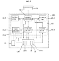
- FIG. 2 is a block diagram illustrating one embodiment 120A of the circuit board 120 illustrated in FIG. 1 .
- the camera module 100 may further include a lens 130.
- the ground portion 122 may be a body itself of the circuit board 120A rather than being a separate member as described above.
- wires G connected between the ground portion 122 and the respective elements 126-1, 126-2, 126-3, 126-4, 126-5, and 126-6 are virtual electric wires representing that the ground portion 122 is in electrical conduction with the respective elements 126-1 to 126-6.
- the ground portion 122 is not in electrical conduction with the connection portion 124 because the connection portion 124 is electrically insulated from the ground portion 122.
- the circuit board 120A illustrated in FIG. 2 may include an image sensor 126-1, an oscillator 126-2, a video amplifier 126-3, a converter 126-4, a storage unit 126-5, and a controller 126-6.
- Each of the elements 126-1 to 126-6 illustrated in FIG. 2 may correspond to at least one functional element 126 illustrated in FIG. 1 .
- the lens 130 focuses an image of a target object to be photographed on the image sensor 126-1.
- the image sensor 126-1 may convert an optical image from the lens 130 into an electrical image signal in response to a clock signal and output the converted electrical image signal to the video amplifier 126-3.
- the oscillator 126-2 may generate a clock signal and output the generated clock signal to the image sensor 126-1.
- the video amplifier 126-3 may amplify the electrical image signal received from the image sensor 126-1 and output the amplified result as a video signal through a signal input/output terminal 124-1 (OUT) of the connection portion 124.
- the converter 126-4 may convert a level of power received from the external device 400 through a power input terminal 124-2 (IN) of the connection portion 124 into a level of power required for the circuit board 120A and output the converted level of power to the respective elements 126-1 to 126-6.
- the converter 126-4 may include at least one of a DC-DC converter (not illustrated) or a Low voltage Drop Out (LDO) regulator (not illustrated).
- the storage unit 126-5 may be connected to the image sensor 126-1 and serve to temporarily store the electrical image signal generated in the image sensor 126-1.
- the storage unit 126-5 may be implemented as a flash memory.
- the controller 126-6 may control at least one of the image sensor 126-1 or the converter 126-4.
- connection portion 124 and the ground portion 122 are electrically insulated from each other, the respective elements 126-1 to 126-6 may be protected from the electrostatic discharge 10 even if the electrostatic discharge 10 is introduced into the connection portion 124 through the housing 110 and the metal 220 of the connector 200.
- the circuit board 120A of the camera module 100 illustrated in FIG. 2 is merely one example for description of the respective elements 126-1 to 126-6 of the circuit board 120A which are protected from the electrostatic discharge 10 and the embodiment is not limited thereto. Thus, even if the circuit board 120A of the camera module 100 in accordance with the embodiment includes any kinds of functional elements, the embodiment may be applied thereto.
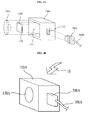
- FIGs. 3A and 3B are respectively an exploded perspective view and an assembled perspective view illustrating a housing 110A, a circuit board 120B, and a lens 130A according to an embodiment.
- the housing 110A and the circuit board 120B may correspond to one embodiment of each of the housing 110 and the circuit board 120 illustrated in FIG. 1
- the lens 130A may correspond to one embodiment of the lens 130 illustrated in FIG. 2 .
- the housing 110A is illustrated as having a hexahedral outer shape, the embodiment is not limited to this external shape of the housing 110A.
- the housing 110A may have first and second openings 111 and 112.
- the first opening 111 may correspond to an opening through which the circuit board 120B is introduced for reception in the housing 110A.
- the second opening 112 may correspond to an opening through which the protrusion 230 of the connector 200 passes for coupling with a connection socket 129 of the connection portion 124 of the circuit board 120B.
- the connector 200 may of course be coupled to the circuit board 120B in a manner different from the illustration of FIGs. 3A and 3B .
- the connector 200 connected to the external device 400 through the cable 300A may be connected to the connection portion 124 of the circuit board 120B through the second opening 112.
- the various functional elements 126-1 to 126-K which are included in the circuit board 120B so as to be in electrical conduction with one another, may be protected from the electrostatic discharge 10 because the connection portion 124 is electrically insulated from the ground portion 122 as described above.
- almost all ICs mounted on the circuit board 120 may be affected by the electrostatic discharge 10.
- FIGs. 3A and 3B are provided by way of example for better understanding of the camera module 100 according to the embodiment and the embodiment is not limited thereto. That is, the circuit board 120 of the camera module 100 according to the embodiment may be protected from the electrostatic discharge 10 regardless of the shapes of and coupling structures between the housing 110, the circuit board 120, and the lens 130 of the camera module 100.
- the embodiment is not limited thereto. That is, the following description may be applied even when the camera module 100 according to the embodiment is applied to other uses, for example, a monitoring camera.
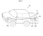
- FIG. 4 is a partially cut-away perspective view illustrating the vehicle 500 equipped with the camera module 100 according to an embodiment.
- the vehicle 500 may include a camera module 100A, a connector 200B, a cable 300B, and an external device 400A.
- the camera module 100A, the connector 200B, the cable 300B, and the external device 400A may respectively correspond to the embodiment of each of the camera module 100, the connector 200, the cable 300, and the external device 400 illustrated in FIG. 1 .
- the external device 400A may include a battery that supplies power to respective components of the vehicle 500. Power may be supplied from the battery 400A to the camera module 100A through the cable 300B and the connector 200B.
- the connector 200B may be connected to the circuit board 120 within the camera module 100A as exemplarily illustrated in FIG. 1 .
- the external device 400A may include an Electronic Control Unit (ECU) that analyzes a surrounding image of the vehicle 500.
- ECU Electronic Control Unit
- a vehicle has any one of various ECUs.
- the ECU may be a sort of a computer containing software that is capable of executing various functions for a vehicle.
- the ECU included in the external device 400A may be a computer that analyzes a surrounding image of the vehicle 500.
- the connector 200B may transmit a surrounding image generated in the camera module 100A to the ECU 400A through the cable 300B.
- the electrostatic discharge 10 may be dissipated through the cable 300B when the length of the cable 300B is sufficiently short.
- the camera module 100A according to the embodiment may protect the circuit board 120 of the camera module 100A from the electrostatic discharge 10 when the length of the cable 300B is long, for example, 10 cm or more or 15 cm or more.
- the camera module 100A may serve as a rear monitoring camera of the vehicle 500, without being limited thereto. According to another embodiment, the camera module 100A may serve as a front surveillance camera differently from the illustration of FIG. 4 .
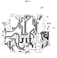
- FIG. 5 is a plan view illustrating the circuit board 120C according to an embodiment.
- the circuit board 120C illustrated in FIG. 5 may include the ground portion 122 and the connection portion 124.
- the ground portion 122 may be a body itself of the circuit board 120C. According to the embodiment, it can be appreciated that the ground portion 122 is electrically floated from the connection portion 124.
- FIGs. 6(a) and 6(b) respectively illustrate a state in which circuit boards according to a comparative embodiment and an embodiment are affected by electrostatic discharge 10.
- the greater the strength of noise caused by electrostatic discharge the greater the level of energy.
- FIG. 7 is a graph illustrating the influence of impedance depending on electrostatic discharge in camera modules according to a comparative embodiment 310 and an embodiment 320.
- the horizontal axis represents frequency and the vertical axis represents the energy level of electrostatic discharge measured in a line of the circuit board.
- the energy level of electrostatic discharge is very high in the case of the comparative embodiment 310 in which a connection portion and a ground portion of a circuit board are connected to each other in the camera module.
- connection portion 124 and the ground portion 122 of the circuit board are electrically floated and the energy level of electrostatic discharge is much lower than that of the comparative embodiment 310.
- the camera module of the embodiment may be a vehicle camera module and may be mounted to a vehicle. That is, the vehicle or vehicle component may include the embodiment.
- a connection portion and a ground portion of a circuit board are electrically floated from each other, even if electrostatic discharge is applied to a housing of the camera module, various functional elements of the circuit board are not affected by noise of the electrostatic discharge.
- the camera module and the vehicle component including the same may achieve a reduced defect rate as well as increased lifespan and may also hereby perform a correct function without being affected by variation of a surrounding environment such as electrostatic discharge.
Landscapes
- Engineering & Computer Science (AREA)
- Multimedia (AREA)
- Signal Processing (AREA)
- Mechanical Engineering (AREA)
- Physics & Mathematics (AREA)
- General Physics & Mathematics (AREA)
- Studio Devices (AREA)
- Camera Bodies And Camera Details Or Accessories (AREA)
Applications Claiming Priority (1)
| Application Number | Priority Date | Filing Date | Title |
|---|---|---|---|
| KR1020140069128A KR102220502B1 (ko) | 2014-06-09 | 2014-06-09 | 카메라 모듈 및 이를 포함하는 차량 부품 |
Publications (2)
| Publication Number | Publication Date |
|---|---|
| EP2955910A1 true EP2955910A1 (de) | 2015-12-16 |
| EP2955910B1 EP2955910B1 (de) | 2020-06-03 |
Family
ID=53189679
Family Applications (1)
| Application Number | Title | Priority Date | Filing Date |
|---|---|---|---|
| EP15167867.9A Active EP2955910B1 (de) | 2014-06-09 | 2015-05-15 | Kameramodul und fahrzeugkomponente damit |
Country Status (4)
| Country | Link |
|---|---|
| US (1) | US20150353025A1 (de) |
| EP (1) | EP2955910B1 (de) |
| KR (1) | KR102220502B1 (de) |
| CN (1) | CN105282410B (de) |
Cited By (1)
| Publication number | Priority date | Publication date | Assignee | Title |
|---|---|---|---|---|
| WO2021061177A1 (en) * | 2019-09-27 | 2021-04-01 | Gm Cruise Holdings Llc | Automotive camera unit |
Families Citing this family (16)
| Publication number | Priority date | Publication date | Assignee | Title |
|---|---|---|---|---|
| KR20170041470A (ko) | 2015-10-07 | 2017-04-17 | 주식회사 엘지화학 | 전극조립체를 구성하는 분리막의 기공 내에 겔화 전해액 성분을 포함하고 있는 전지셀 |
| US11767012B2 (en) | 2017-01-19 | 2023-09-26 | Hl Klemove Corp. | Camera system for intelligent driver assistance system, and driver assistance system and method |
| KR102686601B1 (ko) * | 2017-01-19 | 2024-07-19 | 주식회사 에이치엘클레무브 | Adas를 위한 카메라 시스템 |
| KR102670773B1 (ko) * | 2017-01-19 | 2024-05-30 | 주식회사 에이치엘클레무브 | Adas를 위한 카메라 시스템과 이를 이용한 주행 보조 시스템 |
| KR102766243B1 (ko) * | 2017-01-19 | 2025-02-12 | 주식회사 에이치엘클레무브 | Adas를 위한 카메라 시스템과, 긴급제동 시스템 및 방법 |
| KR102670844B1 (ko) * | 2017-01-19 | 2024-05-30 | 주식회사 에이치엘클레무브 | Adas를 위한 카메라 시스템과 이를 이용한 주행 보조 시스템 |
| KR102691715B1 (ko) * | 2017-01-19 | 2024-08-05 | 주식회사 에이치엘클레무브 | Adas를 위한 카메라 시스템과 이를 이용한 주행 보조 시스템 |
| KR102743908B1 (ko) * | 2017-01-19 | 2024-12-17 | 주식회사 에이치엘클레무브 | Adas를 위한 카메라 시스템 |
| KR102682056B1 (ko) * | 2017-01-19 | 2024-07-05 | 주식회사 에이치엘클레무브 | Adas를 위한 카메라 시스템과 이를 이용한 주행 보조 시스템 |
| KR102669526B1 (ko) * | 2017-01-19 | 2024-05-27 | 주식회사 에이치엘클레무브 | Adas를 위한 카메라 시스템과, 충돌 방지 시스템 및 방법 |
| KR102666315B1 (ko) * | 2017-01-19 | 2024-05-16 | 주식회사 에이치엘클레무브 | Adas를 위한 카메라 시스템과, 교차로 충돌 방지 시스템 및 방법 |
| KR102669183B1 (ko) * | 2017-01-19 | 2024-05-24 | 주식회사 에이치엘클레무브 | Adas를 위한 카메라 시스템과, 차량 제어 장치 및 방법 |
| WO2018135869A1 (ko) | 2017-01-19 | 2018-07-26 | 주식회사 만도 | 지능형 운전자 보조 시스템을 위한 카메라 시스템, 및 운전자 보조 시스템 및 방법 |
| KR102713185B1 (ko) * | 2017-01-19 | 2024-10-04 | 주식회사 에이치엘클레무브 | Adas를 위한 카메라 시스템과, 교차로 충돌 방지 시스템 및 방법 |
| CN111405160B (zh) * | 2020-03-26 | 2021-09-03 | 维沃移动通信有限公司 | 一种摄像头模组及电子设备 |
| USD1065089S1 (en) | 2022-07-25 | 2025-03-04 | Thomas J. Henne | Set of replacement connectors for an engine control module (ECM) |
Citations (4)
| Publication number | Priority date | Publication date | Assignee | Title |
|---|---|---|---|---|
| EP1942661A2 (de) * | 2007-01-08 | 2008-07-09 | VisEra Technologies Company Limited | Elektronische Anordnung für eine Bildsensorvorrichtung und Herstellungsverfahren dafür |
| US20110025850A1 (en) * | 2009-08-03 | 2011-02-03 | Ricoh Company, Ltd. | Camera unit and sensing device |
| WO2012061567A1 (en) * | 2010-11-04 | 2012-05-10 | Magna Electronics Inc. | Vehicular camera system with reduced number of pins and conduits |
| US20140148030A1 (en) * | 2012-11-29 | 2014-05-29 | Smk Corporation | Electrical connection structure between module device and an external device |
Family Cites Families (8)
| Publication number | Priority date | Publication date | Assignee | Title |
|---|---|---|---|---|
| KR20090032228A (ko) * | 2007-09-27 | 2009-04-01 | 엘지이노텍 주식회사 | 카메라 모듈 |
| KR20090064945A (ko) * | 2007-12-17 | 2009-06-22 | 엘지이노텍 주식회사 | 인쇄회로기판 및 이를 구비하는 단말기 |
| US20090187781A1 (en) * | 2008-01-23 | 2009-07-23 | Hella Kg Hueck & Co. | Electronic Control Unit with Power Loss Compensation |
| US20090228640A1 (en) * | 2008-03-07 | 2009-09-10 | Kabushiki Kaisha Toshiba | Information processing apparatus and non-volatile semiconductor memory drive |
| KR20110058019A (ko) * | 2009-11-25 | 2011-06-01 | 김선채 | 후방카메라형 주차보조장치 |
| JP5488839B2 (ja) * | 2011-05-12 | 2014-05-14 | 第一精工株式会社 | コネクタ装置 |
| US9179536B2 (en) * | 2012-05-30 | 2015-11-03 | Lear Corporation | Printed circuit board assembly and solder validation method |
| CN102857680B (zh) * | 2012-08-29 | 2016-02-24 | 惠州Tcl移动通信有限公司 | 摄像组件及配备有该摄像组件的电子设备 |
-
2014
- 2014-06-09 KR KR1020140069128A patent/KR102220502B1/ko active Active
-
2015
- 2015-05-14 US US14/712,410 patent/US20150353025A1/en not_active Abandoned
- 2015-05-15 EP EP15167867.9A patent/EP2955910B1/de active Active
- 2015-06-09 CN CN201510314231.4A patent/CN105282410B/zh active Active
Patent Citations (4)
| Publication number | Priority date | Publication date | Assignee | Title |
|---|---|---|---|---|
| EP1942661A2 (de) * | 2007-01-08 | 2008-07-09 | VisEra Technologies Company Limited | Elektronische Anordnung für eine Bildsensorvorrichtung und Herstellungsverfahren dafür |
| US20110025850A1 (en) * | 2009-08-03 | 2011-02-03 | Ricoh Company, Ltd. | Camera unit and sensing device |
| WO2012061567A1 (en) * | 2010-11-04 | 2012-05-10 | Magna Electronics Inc. | Vehicular camera system with reduced number of pins and conduits |
| US20140148030A1 (en) * | 2012-11-29 | 2014-05-29 | Smk Corporation | Electrical connection structure between module device and an external device |
Cited By (2)
| Publication number | Priority date | Publication date | Assignee | Title |
|---|---|---|---|---|
| WO2021061177A1 (en) * | 2019-09-27 | 2021-04-01 | Gm Cruise Holdings Llc | Automotive camera unit |
| US11148611B2 (en) | 2019-09-27 | 2021-10-19 | GM Cruise Holdings, LLC | Automotive camera unit |
Also Published As
| Publication number | Publication date |
|---|---|
| CN105282410B (zh) | 2020-02-28 |
| KR102220502B1 (ko) | 2021-02-25 |
| KR20150140927A (ko) | 2015-12-17 |
| CN105282410A (zh) | 2016-01-27 |
| US20150353025A1 (en) | 2015-12-10 |
| EP2955910B1 (de) | 2020-06-03 |
Similar Documents
| Publication | Publication Date | Title |
|---|---|---|
| EP2955910B1 (de) | Kameramodul und fahrzeugkomponente damit | |
| US11418688B2 (en) | Camera module for use in automobile | |
| KR102248086B1 (ko) | 자동차용 카메라 모듈 | |
| KR20230027134A (ko) | 카메라 모듈 | |
| KR102500655B1 (ko) | 카메라 모듈 및 이를 포함하는 자동차 | |
| US10795111B2 (en) | Camera module and vehicle comprising same | |
| KR102324878B1 (ko) | 카메라 모듈 및 자동차 | |
| KR102371355B1 (ko) | 차량용 카메라 | |
| KR102500367B1 (ko) | 카메라 모듈 및 자동차 | |
| KR20190012339A (ko) | 카메라 모듈 및 자동차 | |
| US10609261B2 (en) | Optical camera to be mounted on vehicles | |
| EP2863623A1 (de) | Fahrzeugkamera mit verbesserter Verbindungsvorrichtung und Kraftfahrzeug | |
| KR102411132B1 (ko) | 카메라 모듈 | |
| KR102619128B1 (ko) | 카메라 모듈 | |
| KR102361050B1 (ko) | 카메라 모듈 및 제조장치 | |
| EP3080979B1 (de) | Elektronische vorrichtung mit verbessertem lager für eine verbindungseinheit, kamerasystem für ein kraftfahrzeug und kraftfahrzeug | |
| KR20200076347A (ko) | 카메라 모듈 | |
| KR20210052418A (ko) | 자동차용 카메라 모듈 |
Legal Events
| Date | Code | Title | Description |
|---|---|---|---|
| PUAI | Public reference made under article 153(3) epc to a published international application that has entered the european phase |
Free format text: ORIGINAL CODE: 0009012 |
|
| AK | Designated contracting states |
Kind code of ref document: A1 Designated state(s): AL AT BE BG CH CY CZ DE DK EE ES FI FR GB GR HR HU IE IS IT LI LT LU LV MC MK MT NL NO PL PT RO RS SE SI SK SM TR |
|
| AX | Request for extension of the european patent |
Extension state: BA ME |
|
| 17P | Request for examination filed |
Effective date: 20160216 |
|
| RBV | Designated contracting states (corrected) |
Designated state(s): AL AT BE BG CH CY CZ DE DK EE ES FI FR GB GR HR HU IE IS IT LI LT LU LV MC MK MT NL NO PL PT RO RS SE SI SK SM TR |
|
| STAA | Information on the status of an ep patent application or granted ep patent |
Free format text: STATUS: EXAMINATION IS IN PROGRESS |
|
| RAP1 | Party data changed (applicant data changed or rights of an application transferred) |
Owner name: LG INNOTEK CO., LTD. |
|
| 17Q | First examination report despatched |
Effective date: 20170515 |
|
| GRAP | Despatch of communication of intention to grant a patent |
Free format text: ORIGINAL CODE: EPIDOSNIGR1 |
|
| STAA | Information on the status of an ep patent application or granted ep patent |
Free format text: STATUS: GRANT OF PATENT IS INTENDED |
|
| INTG | Intention to grant announced |
Effective date: 20191218 |
|
| GRAS | Grant fee paid |
Free format text: ORIGINAL CODE: EPIDOSNIGR3 |
|
| GRAA | (expected) grant |
Free format text: ORIGINAL CODE: 0009210 |
|
| STAA | Information on the status of an ep patent application or granted ep patent |
Free format text: STATUS: THE PATENT HAS BEEN GRANTED |
|
| AK | Designated contracting states |
Kind code of ref document: B1 Designated state(s): AL AT BE BG CH CY CZ DE DK EE ES FI FR GB GR HR HU IE IS IT LI LT LU LV MC MK MT NL NO PL PT RO RS SE SI SK SM TR |
|
| REG | Reference to a national code |
Ref country code: GB Ref legal event code: FG4D |
|
| REG | Reference to a national code |
Ref country code: CH Ref legal event code: EP Ref country code: AT Ref legal event code: REF Ref document number: 1278286 Country of ref document: AT Kind code of ref document: T Effective date: 20200615 |
|
| REG | Reference to a national code |
Ref country code: DE Ref legal event code: R096 Ref document number: 602015053643 Country of ref document: DE |
|
| REG | Reference to a national code |
Ref country code: NL Ref legal event code: FP |
|
| REG | Reference to a national code |
Ref country code: LT Ref legal event code: MG4D |
|
| PG25 | Lapsed in a contracting state [announced via postgrant information from national office to epo] |
Ref country code: FI Free format text: LAPSE BECAUSE OF FAILURE TO SUBMIT A TRANSLATION OF THE DESCRIPTION OR TO PAY THE FEE WITHIN THE PRESCRIBED TIME-LIMIT Effective date: 20200603 Ref country code: SE Free format text: LAPSE BECAUSE OF FAILURE TO SUBMIT A TRANSLATION OF THE DESCRIPTION OR TO PAY THE FEE WITHIN THE PRESCRIBED TIME-LIMIT Effective date: 20200603 Ref country code: LT Free format text: LAPSE BECAUSE OF FAILURE TO SUBMIT A TRANSLATION OF THE DESCRIPTION OR TO PAY THE FEE WITHIN THE PRESCRIBED TIME-LIMIT Effective date: 20200603 Ref country code: NO Free format text: LAPSE BECAUSE OF FAILURE TO SUBMIT A TRANSLATION OF THE DESCRIPTION OR TO PAY THE FEE WITHIN THE PRESCRIBED TIME-LIMIT Effective date: 20200903 Ref country code: GR Free format text: LAPSE BECAUSE OF FAILURE TO SUBMIT A TRANSLATION OF THE DESCRIPTION OR TO PAY THE FEE WITHIN THE PRESCRIBED TIME-LIMIT Effective date: 20200904 |
|
| PG25 | Lapsed in a contracting state [announced via postgrant information from national office to epo] |
Ref country code: BG Free format text: LAPSE BECAUSE OF FAILURE TO SUBMIT A TRANSLATION OF THE DESCRIPTION OR TO PAY THE FEE WITHIN THE PRESCRIBED TIME-LIMIT Effective date: 20200903 Ref country code: RS Free format text: LAPSE BECAUSE OF FAILURE TO SUBMIT A TRANSLATION OF THE DESCRIPTION OR TO PAY THE FEE WITHIN THE PRESCRIBED TIME-LIMIT Effective date: 20200603 Ref country code: LV Free format text: LAPSE BECAUSE OF FAILURE TO SUBMIT A TRANSLATION OF THE DESCRIPTION OR TO PAY THE FEE WITHIN THE PRESCRIBED TIME-LIMIT Effective date: 20200603 Ref country code: HR Free format text: LAPSE BECAUSE OF FAILURE TO SUBMIT A TRANSLATION OF THE DESCRIPTION OR TO PAY THE FEE WITHIN THE PRESCRIBED TIME-LIMIT Effective date: 20200603 |
|
| REG | Reference to a national code |
Ref country code: AT Ref legal event code: MK05 Ref document number: 1278286 Country of ref document: AT Kind code of ref document: T Effective date: 20200603 |
|
| PG25 | Lapsed in a contracting state [announced via postgrant information from national office to epo] |
Ref country code: AL Free format text: LAPSE BECAUSE OF FAILURE TO SUBMIT A TRANSLATION OF THE DESCRIPTION OR TO PAY THE FEE WITHIN THE PRESCRIBED TIME-LIMIT Effective date: 20200603 |
|
| PG25 | Lapsed in a contracting state [announced via postgrant information from national office to epo] |
Ref country code: AT Free format text: LAPSE BECAUSE OF FAILURE TO SUBMIT A TRANSLATION OF THE DESCRIPTION OR TO PAY THE FEE WITHIN THE PRESCRIBED TIME-LIMIT Effective date: 20200603 Ref country code: ES Free format text: LAPSE BECAUSE OF FAILURE TO SUBMIT A TRANSLATION OF THE DESCRIPTION OR TO PAY THE FEE WITHIN THE PRESCRIBED TIME-LIMIT Effective date: 20200603 Ref country code: EE Free format text: LAPSE BECAUSE OF FAILURE TO SUBMIT A TRANSLATION OF THE DESCRIPTION OR TO PAY THE FEE WITHIN THE PRESCRIBED TIME-LIMIT Effective date: 20200603 Ref country code: SM Free format text: LAPSE BECAUSE OF FAILURE TO SUBMIT A TRANSLATION OF THE DESCRIPTION OR TO PAY THE FEE WITHIN THE PRESCRIBED TIME-LIMIT Effective date: 20200603 Ref country code: RO Free format text: LAPSE BECAUSE OF FAILURE TO SUBMIT A TRANSLATION OF THE DESCRIPTION OR TO PAY THE FEE WITHIN THE PRESCRIBED TIME-LIMIT Effective date: 20200603 Ref country code: IT Free format text: LAPSE BECAUSE OF FAILURE TO SUBMIT A TRANSLATION OF THE DESCRIPTION OR TO PAY THE FEE WITHIN THE PRESCRIBED TIME-LIMIT Effective date: 20200603 Ref country code: CZ Free format text: LAPSE BECAUSE OF FAILURE TO SUBMIT A TRANSLATION OF THE DESCRIPTION OR TO PAY THE FEE WITHIN THE PRESCRIBED TIME-LIMIT Effective date: 20200603 Ref country code: PT Free format text: LAPSE BECAUSE OF FAILURE TO SUBMIT A TRANSLATION OF THE DESCRIPTION OR TO PAY THE FEE WITHIN THE PRESCRIBED TIME-LIMIT Effective date: 20201006 |
|
| PG25 | Lapsed in a contracting state [announced via postgrant information from national office to epo] |
Ref country code: SK Free format text: LAPSE BECAUSE OF FAILURE TO SUBMIT A TRANSLATION OF THE DESCRIPTION OR TO PAY THE FEE WITHIN THE PRESCRIBED TIME-LIMIT Effective date: 20200603 Ref country code: PL Free format text: LAPSE BECAUSE OF FAILURE TO SUBMIT A TRANSLATION OF THE DESCRIPTION OR TO PAY THE FEE WITHIN THE PRESCRIBED TIME-LIMIT Effective date: 20200603 Ref country code: IS Free format text: LAPSE BECAUSE OF FAILURE TO SUBMIT A TRANSLATION OF THE DESCRIPTION OR TO PAY THE FEE WITHIN THE PRESCRIBED TIME-LIMIT Effective date: 20201003 |
|
| REG | Reference to a national code |
Ref country code: DE Ref legal event code: R097 Ref document number: 602015053643 Country of ref document: DE |
|
| PLBE | No opposition filed within time limit |
Free format text: ORIGINAL CODE: 0009261 |
|
| STAA | Information on the status of an ep patent application or granted ep patent |
Free format text: STATUS: NO OPPOSITION FILED WITHIN TIME LIMIT |
|
| PG25 | Lapsed in a contracting state [announced via postgrant information from national office to epo] |
Ref country code: DK Free format text: LAPSE BECAUSE OF FAILURE TO SUBMIT A TRANSLATION OF THE DESCRIPTION OR TO PAY THE FEE WITHIN THE PRESCRIBED TIME-LIMIT Effective date: 20200603 |
|
| 26N | No opposition filed |
Effective date: 20210304 |
|
| PG25 | Lapsed in a contracting state [announced via postgrant information from national office to epo] |
Ref country code: SI Free format text: LAPSE BECAUSE OF FAILURE TO SUBMIT A TRANSLATION OF THE DESCRIPTION OR TO PAY THE FEE WITHIN THE PRESCRIBED TIME-LIMIT Effective date: 20200603 |
|
| REG | Reference to a national code |
Ref country code: CH Ref legal event code: PL |
|
| GBPC | Gb: european patent ceased through non-payment of renewal fee |
Effective date: 20210515 |
|
| PG25 | Lapsed in a contracting state [announced via postgrant information from national office to epo] |
Ref country code: MC Free format text: LAPSE BECAUSE OF FAILURE TO SUBMIT A TRANSLATION OF THE DESCRIPTION OR TO PAY THE FEE WITHIN THE PRESCRIBED TIME-LIMIT Effective date: 20200603 Ref country code: LU Free format text: LAPSE BECAUSE OF NON-PAYMENT OF DUE FEES Effective date: 20210515 Ref country code: LI Free format text: LAPSE BECAUSE OF NON-PAYMENT OF DUE FEES Effective date: 20210531 Ref country code: CH Free format text: LAPSE BECAUSE OF NON-PAYMENT OF DUE FEES Effective date: 20210531 |
|
| REG | Reference to a national code |
Ref country code: BE Ref legal event code: MM Effective date: 20210531 |
|
| PG25 | Lapsed in a contracting state [announced via postgrant information from national office to epo] |
Ref country code: IE Free format text: LAPSE BECAUSE OF NON-PAYMENT OF DUE FEES Effective date: 20210515 Ref country code: GB Free format text: LAPSE BECAUSE OF NON-PAYMENT OF DUE FEES Effective date: 20210515 |
|
| PG25 | Lapsed in a contracting state [announced via postgrant information from national office to epo] |
Ref country code: BE Free format text: LAPSE BECAUSE OF NON-PAYMENT OF DUE FEES Effective date: 20210531 |
|
| REG | Reference to a national code |
Ref country code: DE Ref legal event code: R079 Ref document number: 602015053643 Country of ref document: DE Free format text: PREVIOUS MAIN CLASS: H04N0005225000 Ipc: H04N0023000000 |
|
| PG25 | Lapsed in a contracting state [announced via postgrant information from national office to epo] |
Ref country code: HU Free format text: LAPSE BECAUSE OF FAILURE TO SUBMIT A TRANSLATION OF THE DESCRIPTION OR TO PAY THE FEE WITHIN THE PRESCRIBED TIME-LIMIT; INVALID AB INITIO Effective date: 20150515 |
|
| PG25 | Lapsed in a contracting state [announced via postgrant information from national office to epo] |
Ref country code: CY Free format text: LAPSE BECAUSE OF FAILURE TO SUBMIT A TRANSLATION OF THE DESCRIPTION OR TO PAY THE FEE WITHIN THE PRESCRIBED TIME-LIMIT Effective date: 20200603 |
|
| PG25 | Lapsed in a contracting state [announced via postgrant information from national office to epo] |
Ref country code: MK Free format text: LAPSE BECAUSE OF FAILURE TO SUBMIT A TRANSLATION OF THE DESCRIPTION OR TO PAY THE FEE WITHIN THE PRESCRIBED TIME-LIMIT Effective date: 20200603 |
|
| PG25 | Lapsed in a contracting state [announced via postgrant information from national office to epo] |
Ref country code: TR Free format text: LAPSE BECAUSE OF FAILURE TO SUBMIT A TRANSLATION OF THE DESCRIPTION OR TO PAY THE FEE WITHIN THE PRESCRIBED TIME-LIMIT Effective date: 20200603 |
|
| PG25 | Lapsed in a contracting state [announced via postgrant information from national office to epo] |
Ref country code: MT Free format text: LAPSE BECAUSE OF FAILURE TO SUBMIT A TRANSLATION OF THE DESCRIPTION OR TO PAY THE FEE WITHIN THE PRESCRIBED TIME-LIMIT Effective date: 20200603 |
|
| PGFP | Annual fee paid to national office [announced via postgrant information from national office to epo] |
Ref country code: NL Payment date: 20250422 Year of fee payment: 11 |
|
| PGFP | Annual fee paid to national office [announced via postgrant information from national office to epo] |
Ref country code: DE Payment date: 20250422 Year of fee payment: 11 |
|
| PGFP | Annual fee paid to national office [announced via postgrant information from national office to epo] |
Ref country code: FR Payment date: 20250422 Year of fee payment: 11 |