EP1949147B1 - Procede destine a la production d un element de reseau de diffraction - Google Patents
Procede destine a la production d un element de reseau de diffraction Download PDFInfo
- Publication number
- EP1949147B1 EP1949147B1 EP05812973A EP05812973A EP1949147B1 EP 1949147 B1 EP1949147 B1 EP 1949147B1 EP 05812973 A EP05812973 A EP 05812973A EP 05812973 A EP05812973 A EP 05812973A EP 1949147 B1 EP1949147 B1 EP 1949147B1
- Authority
- EP
- European Patent Office
- Prior art keywords
- mold
- grating
- equal
- diffraction grating
- grooves
- Prior art date
- Legal status (The legal status is an assumption and is not a legal conclusion. Google has not performed a legal analysis and makes no representation as to the accuracy of the status listed.)
- Expired - Lifetime
Links
Images




Classifications
-
- G—PHYSICS
- G02—OPTICS
- G02B—OPTICAL ELEMENTS, SYSTEMS OR APPARATUS
- G02B5/00—Optical elements other than lenses
- G02B5/18—Diffraction gratings
- G02B5/1847—Manufacturing methods
- G02B5/1852—Manufacturing methods using mechanical means, e.g. ruling with diamond tool, moulding
-
- B—PERFORMING OPERATIONS; TRANSPORTING
- B29—WORKING OF PLASTICS; WORKING OF SUBSTANCES IN A PLASTIC STATE IN GENERAL
- B29D—PRODUCING PARTICULAR ARTICLES FROM PLASTICS OR FROM SUBSTANCES IN A PLASTIC STATE
- B29D11/00—Producing optical elements, e.g. lenses or prisms
- B29D11/0074—Production of other optical elements not provided for in B29D11/00009- B29D11/0073
- B29D11/00769—Producing diffraction gratings
-
- B—PERFORMING OPERATIONS; TRANSPORTING
- B82—NANOTECHNOLOGY
- B82Y—SPECIFIC USES OR APPLICATIONS OF NANOSTRUCTURES; MEASUREMENT OR ANALYSIS OF NANOSTRUCTURES; MANUFACTURE OR TREATMENT OF NANOSTRUCTURES
- B82Y10/00—Nanotechnology for information processing, storage or transmission, e.g. quantum computing or single electron logic
-
- B—PERFORMING OPERATIONS; TRANSPORTING
- B82—NANOTECHNOLOGY
- B82Y—SPECIFIC USES OR APPLICATIONS OF NANOSTRUCTURES; MEASUREMENT OR ANALYSIS OF NANOSTRUCTURES; MANUFACTURE OR TREATMENT OF NANOSTRUCTURES
- B82Y40/00—Manufacture or treatment of nanostructures
-
- G—PHYSICS
- G03—PHOTOGRAPHY; CINEMATOGRAPHY; ANALOGOUS TECHNIQUES USING WAVES OTHER THAN OPTICAL WAVES; ELECTROGRAPHY; HOLOGRAPHY
- G03F—PHOTOMECHANICAL PRODUCTION OF TEXTURED OR PATTERNED SURFACES, e.g. FOR PRINTING, FOR PROCESSING OF SEMICONDUCTOR DEVICES; MATERIALS THEREFOR; ORIGINALS THEREFOR; APPARATUS SPECIALLY ADAPTED THEREFOR
- G03F7/00—Photomechanical, e.g. photolithographic, production of textured or patterned surfaces, e.g. printing surfaces; Materials therefor, e.g. comprising photoresists; Apparatus specially adapted therefor
- G03F7/0002—Lithographic processes using patterning methods other than those involving the exposure to radiation, e.g. by stamping
-
- G—PHYSICS
- G03—PHOTOGRAPHY; CINEMATOGRAPHY; ANALOGOUS TECHNIQUES USING WAVES OTHER THAN OPTICAL WAVES; ELECTROGRAPHY; HOLOGRAPHY
- G03F—PHOTOMECHANICAL PRODUCTION OF TEXTURED OR PATTERNED SURFACES, e.g. FOR PRINTING, FOR PROCESSING OF SEMICONDUCTOR DEVICES; MATERIALS THEREFOR; ORIGINALS THEREFOR; APPARATUS SPECIALLY ADAPTED THEREFOR
- G03F7/00—Photomechanical, e.g. photolithographic, production of textured or patterned surfaces, e.g. printing surfaces; Materials therefor, e.g. comprising photoresists; Apparatus specially adapted therefor
- G03F7/0005—Production of optical devices or components in so far as characterised by the lithographic processes or materials used therefor
Definitions
- the present invention relates to the production of optical diffraction gratings.
- Diffraction gratings are used in optics to couple light in or out from waveguiding structures. Diffraction gratings may also be used to provide angular dispersion of light comprising several wavelengths.
- US patent 6,579,477 discloses a method for fabricating diffractive optical components by replication using a matrix.
- the matrix is treated with a release agent.
- a substrate is treated with an adhesion promoter and covered with a copy material.
- the matrix is pressed to heated copy material in order to replicate the profile of the matrix.
- US patent 5,629,804 discloses a diffraction grating constituted by a substrate and a resin layer having a repetitive pattern formed on the substrate.
- the repetitive pattern is formed by hardening photo-curable resin in a mold.
- US Patent 4,235,654 discloses a method for producing composite optical elements of glass and polymer material.
- a glass substrate is treated with a silanizing agent to activate its surface.
- An organic polymer material is applied to the activated surface with a mold platen forming the desired exterior configuration.
- the polymer material is cured, and the product, e.g. a diffraction grating, is subsequently released from the mold.
- US patent 5,742,433 discloses a diffractive optical device comprising a grating section, which has several different grating periods. According to the teachings of US patent 5,742,433 , the grating section may be mass-produced by forming a nickel mold by an electroforming method, and by duplicating the mold using UV curable resin.
- US 2001/0008741 A1 discloses manufacturing gratings by exposing a resist layer by light through a mask.
- the resulted grating can also be used as an original to manufacture more gratings by pouring curable resin on the grating and curing the resin, after which the resin is separated from the original by means of a transfer substrate.
- US 6079228 A discloses manufacturing processes for forming glass elements, possibly comprising binary or triangle gratings, by pressing glass softened by heat between two opposite molds.
- the object of the present invention is to provide a method of producing optical diffraction gratings.
- a diffraction grating is produced by using a mold which has a plurality of adjacent microscopic grooves, the inclination of said grooves being greater than or equal to 20 degrees and smaller than or equal to 70 degrees with respect to the normal of the plane of the mold, the depth of the grooves being greater than or equal to 0.4 times the grating period of the mold, the grating period of said mold being greater than or equal to 0.2 ⁇ m and smaller than or equal to 10 ⁇ m, and the clearance angle of said grooves being greater than 0 degrees and smaller than or equal to 20 degrees.
- the method of producing the diffraction grating comprises at least:
- the optical diffraction grating is produced by providing a mold having a plurality of relatively deep inclined grooves, which have a relatively small clearance angle.
- the mold is covered with an anti-adhesion layer.
- the mold is covered with a curable material which is subsequently cured, i.e. hardened, and separated from the mold to provide the diffraction grating.
- the inclined orientation of the grooves allows lateral expansion and/or contraction of the grating during the curing and/or separation steps such that the probability of mold breakage may be reduced.
- the inclined orientation of the grooves may also facilitate the separation of the diffraction grating from the mold.
- the method according to the present invention is suitable for mass production of optical diffraction gratings using molds which have a low clearance angle, and which have a relatively great groove depth with respect to the grating period.
- a mold 50 comprises a profiled surface consisting of a plurality of inclined micro-protrusions 57.
- the micro-protrusions 57 define a plurality of microgrooves 58 between them.
- the mold may be e.g. silica (SiO 2 ) plate.
- a mask may be implemented on the surface of the plate by e.g. electron beam lithography, and the surface relief may be implemented on the masked surface by e.g. reactive ion etching (RIE) or reactive ion beam etching (RIBE).
- RIE reactive ion etching
- RIBE reactive ion beam etching
- Anti-adhesion agent M2 is applied to the mold surface in order to implement an anti-adhesion layer 30.
- the anti-adhesion layer 30 facilitates later removal of the produced grating from the mold 50.
- the orientation of the microgrooves 58 with respect to the normal N of the profiled surface, i.e. the inclination angle ⁇ is greater than or equal to 20° and smaller than or equal to 70°.
- the mold 50 may also be nickel or chromium plate on which the relief is implemented by galvanic methods.
- an amount of curable substance M1 is applied to the profiled surface of the mold 50 in order to cover the surface.
- the substance M1 may be e.g. a droplet of thermally or UV-curable resin.
- the substance M1 may be applied in vacuum in order to avoid entrainment of gas bubbles.
- the spreading of the substance M1 may be assisted by spinning the mold 50.
- the curable substance M1 is cured in the mold 50 in order to form the diffraction grating 10.
- the substance and/or the mold 50 may be heated, or the substance may be exposed to UV radiation.
- the microgrooves 58 of the mold 50 define the form of the respective micro-protrusions of the grating 10.
- the diffraction grating 10 may be separated from the mold 50 by applying a separating force F1.
- one side of the microgroove 58 of the mold 50 is at an angle ⁇ with respect to the normal N of the grating plane.
- the other side of the microgroove 58 is at an angle ⁇ with respect to the normal N.
- the microgrooves 58 have a clearance angle ⁇ in order to facilitate the separation of the grating 10 from the mold 50.
- the clearance angle ⁇ is equal to the difference ⁇ - ⁇ .
- the grating constant d denotes the distance between the positions of the adjacent microgrooves 58.
- s2 denotes the width of the top of the micro-protrusions 57 of the mold 50.
- s1 denotes the width of the top of the micro-protrusions 7 of the produced diffraction grating 10.
- the filling factors c1 and c2 may be e.g. in the range 0.2 to 0.8.
- the grating period may be e.g. in the range of 0.2 ⁇ m to 10 ⁇ m.
- the parameters of the mold 50 are as follows:
- the parameters of the mold 50 are as follows:
- Said range 25° to 45° represents an optimum with respect to the production of the mold 50, and with respect to the separation of the grating 10 from the mold 50.
- the parameter values ⁇ , ⁇ , ⁇ , ⁇ , d and h of the produced diffraction grating 10 are substantially equal to the respective values of the mold 50.
- the diffraction grating 10 is produced using a heat-curable resinous composition.
- the mold 50 having the inclined microgrooves 58 is produced by etching a plate of silica SiO 2 by reactive ion beam etching (RIBE).
- RIBE reactive ion beam etching
- a chromium mask having thickness 10 to 100 nm may be implemented on the silica plate prior to the etching process to define the grating pattern.
- the surface of the mold 50 is covered with an anti-adhesion layer 30, which may be applied as follows:
- a substrate plate 20 having a thickness 0.5 to 3 mm may be manufactured by curing e.g. episulfide-based resinous composition.
- An optimum resinous composition may be selected e.g. from examples disclosed in US patent 6,117,923 .
- the episulfide-based resinous composition is cured thermally by heating.
- the cured resinous composition may have a relatively high refractive index and low optical absorbance.
- an amount of the episulfide-based resinous composition is positioned between the mold 50 and the substrate 20 such that the gap between is filled.
- the resinous composition is cured thermally by heating. Consequently, the grating 10 is joined to the plate 20.
- the produced diffraction grating 10 may be separated from the mold 50 by lifting the edge of the substrate plate 20.
- the substrate improves the mechanical strength of the diffraction grating 10 and facilitates the separation from the mold 50.
- the diffraction grating 10 may be separated from the mold 50 when the substance M1 of the grating 10 is still in semi-hardened state.
- the substance may be only partially cured. Consequently, the protrusions 7 of the grating 10 are soft and flexible, which facilitates the separation of the grating 10 from the mold 50 and further reduces the probability of mold breakage.
- a further advantage associated with the separation in the semi-hardened state is that production rate may be increased.
- the grating 10 may be fully hardened at a later stage, e.g. in an oven.
- the substance M1 of the grating 10 may also be completely cured i.e. completely hardened in the mold 50.
- the protrusions 7 of the grating 10 may be kept soft and flexible also by heating. Thus, the diffraction grating 10 may be separated from the mold 50 when the grating 10 is warm or heated.
- the temperature of the grating 10 may be e.g. greater than or equal to 50°C.
- the diffraction grating 10 may be produced using a UV-curable substance.
- a material under the trade name "NOA61” by the company “Norland Products” may be used.
- the mold 50 is produced and coated with the anti-adhesive layer as described above.
- An amount of "NOA61” is positioned between the substrate 20 and the mould 50, and cured by UV (ultraviolet) radiation.
- the substrate may be e.g. polycarbonate or acrylate polymer.
- the substrate 20 or the mold 50 has to be transparent to UV radiation.
- the surface of the substrate 20 may be activated to improve adhesion between the substrate 20 and the grating 10.
- a further primer layer may be used to improve adhesion between the substrate 20 and the grating 10.
- UV-curable acrylates The fabrication of a silica mold and the use of UV-curable acrylates is also disclosed in an article " 3D microstructure replication processes using UV-curable acrylates", by C.Elsner, J.Dienelt, and D. Hirsch, Microelectronics Engineering Vol. 65 (2003) pp. 163-170 . Also other UV-curable substances provided e.g. by a company "Mitsubishi Gas Chemical Company Inc” may be used.
- the anti-adhesive layer 30 may also be implemented by plasma polymerization or ion sputtering of fluoropolymer films.
- UV-curable materials may be removed from the mold in the semi-hardened state, and the curing of the substance may be completed at a later stage.
- the separation of the diffraction grating 10 from the mold 50 is facilitated by joining the slightly flexible substrate plate 20 to the diffraction grating 10, which allows the combination of the diffraction grating 10 and the substrate 20 to slightly bend in the separation step.
- the thickness of the substrate may be smaller than or equal to 0.1 times the width of the diffraction grating 10 to be produced, in order to allow bending.
- the diffraction grating 10 and the mold 50 may be separated by directing a separating force F2 only to the edge or to the corner of the substrate 20, i.e. by pulling the edge.
- the slight bending of the combination of the diffraction grating 10 and the substrate 20 is advantageous, as it substantially reduces the forces needed to separate the diffraction grating 10 from the mould 50. Thus, one does not need to overcome the adhesive force of the whole area at a time.
- the bottom side of the diffraction grating 10 on the mold side is slightly expanded, which causes a slight sideways displacement of the grating 10 in the direction SX.
- the protrusions 7 of the diffraction grating 10 may slide in the microgrooves 58 of the mold 50 such that the sideways displacement may result as a local separation of the grating 10 and the mold 50, instead of damaging the mold 50 and/or the grating 10.
- the diffraction grating 10 may expand or contract also due to chemical reactions and/or thermal expansion. Also in that case the micro-protrusions 7, 57 are subject to lateral forces. Referring to Fig. 9a , when the diffraction grating is expanded, the protrusions 7 of the diffraction grating 10 may slide in the microgrooves 58 of the mold 50 such that the sideways displacement may result as a local separation of the grating 10 and the mold 50, instead of damaging the mold 50 and/or the grating 10.
- the substance of the grating 10 may also contract when it is cured.
- the protrusions 7 of the diffraction grating 10 may slide in the microgrooves 58 of the mold 50 such that the sideways displacement may result as a local separation of the grating 10 and the mold 50, instead of damaging the mold 50 and/or the grating 10.
- the inclined microgrooves 58 may also facilitate the separation of the grating 10 from the mold 50. It may be that the structure is pre-stressed due to the contraction such that just a small impact or very small separative movement is enough to completely separate the grating 10 from the mold 50, without a need to apply a great and external separative force. In other words, thanks to the inclined orientation of the microgrooves 58, the separation may be surprisingly easy.
- the expansion of the grating 10 may lead to breaking of the mold 50 if the microgrooves 58 are substantially perpendicular to the grating plane, and the clearance angle is small. Also the produced grating 10 may be damaged. Furthermore, the broken pieces of the protrusions may clog one or more microgrooves of the mold 50.
- the method according to the present invention reduces the probability that the mold 50 is damaged during the curing and/or separation steps due to lateral deformations.
- Thermal expansion/contraction, expansion/contraction due to chemical reactions, and expansion/contraction due to bending may now be allowed due to the inclined orientation of the microgrooves 58.
- Fig. 11 shows a microscope image of a diffraction grating produced by a method according to the present invention.
- the grating is made of episulfide-based resinous composition.
- the inclination angle of the protrusions is 25°
- the height of the protrusions is 261 nm
- the grating period is 480 nm
- the fill factor is 0.66
- the clearance angle is 10°.
- Fig. 12 shows a microscope image of a diffraction grating produced by a method according to the present invention.
- the grating is made of episulfide-based resinous composition.
- the inclination angle of the protrusions is 35 °.
- the tops of the protrusions have a rounded form in order to further facilitate separation of the grating from the mold.
- m is the diffraction order (an integer assuming values ...-3, -2, - 1, 0, 1, 2, 3... )
- ⁇ . is the wavelength of the incident light
- ⁇ i is the angle between the direction of the light impinging on the grating and the surface normal N
- ⁇ m is the angle between direction of the diffracted light and the surface normal N.
- n is the refractive index of the grating material.
- L1 denotes the incoming light beam and L2 denotes one of the diffracted beams.
- the produced diffraction grating 10 may be used to change the direction of a light beam L1 impinging on the grating 10.
- the produced diffraction grating 10 may also be used to provide angular dispersion of light impinging on the grating 10, said light comprising several wavelengths.
- the grating period d, the groove depth h, the filling factor c1, and the inclination angle ⁇ are selected according to the optical application.
- the minimization of the clearance angle may provide best optical performance, but may also increase the probability of mold breakage.
- the optimum clearance angle my may be established by a series of experimental tests.
- the diffraction grating 10 produced according to the present invention may be optimized and used e.g. to couple light L1 into an optical waveguide 200.
- the direction of propagation of the light L1 may be substantially perpendicular to the waveguide 200.
- the direction of the light is changed by the grating 10 such that the diffracted light L2 is confined within the waveguide 200.
- the waveguide 200 may further comprise a cladding layer (not shown)
- the mold 50 may comprise several micro structured areas A1, A2, in which the inclination angles ⁇ 1, ⁇ 2 of the microgrooves 58 are different.
- the inclination angle ⁇ 1 may be 10°
- the inclination angle ⁇ 2 may be 20°.
- the expansion of the grating 10 leads to separation of the grating 10 from the mould 50, instead of breaking the protrusions 57 of the mold 50.
- the width s3 of the non-structured area A3 may be e.g. 50 times the grating period d.
- the difference between the inclination angles of adjacent microgrooves 58 may also be so small that the intermediate area A3 is not needed.
- the grating 10 may be separated from the mold 50 thanks to the expansion or contraction of the curable substance.
- the micro-protrusions 7 may also be slightly flexible when they are in the heated and/or semi-hardened state, which facilitates the separation when the adjacent microgrooves 58 have different inclination angles.
- the microgrooves may be inclined to opposite directions, e.g. the inclination angle ⁇ 1 may be 20° anti-clockwise in the first area A1 and the inclination angle ⁇ 2 may be 20° clockwise in the second area A1.
- the diffraction grating 10 may be used implement a diffractive lens 60, which directs light by diffraction.
- the diffractive lens 60 may be used e.g. for imaging and/or to focus parallel light rays L1 to a focal point 62.
- the mold 50 for producing the diffractive lens 60 according to Fig. 17 may comprise circular and/or curved microgrooves 58.
- the substance of the diffraction grating may contract when said substance is cured.
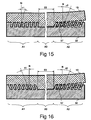
- the inclined orientation of the microgrooves 58a, 58b may facilitate the separation of the diffraction grating 10 from the mold 50 and/or to reduce the probability of mold breakage.
- the protrusions 7 of the grating 10 may slide in the microgrooves 58a, 58b.
- a lateral movement of the grating edge in the direction SX may be associated with a separating movement in the direction SY when the substance is contracted.
- the relative orientation of the microgrooves 58 may also be such that a slight expansion of the diffractive lens 60 is required for the separation of the lens 60 from the mold 50.
- the curable material of the lens may be expanded e.g. by heating.
- the diffractive lens 60 may be a diverging lens, i.e. it may have a negative focal length.
- the protrusions 7 of the grating 10 may slide in the microgrooves 58a, 58b, and the lateral movement of the grating edge in the direction SX may be associated with a separating movement in the direction SY when the curable substance of the lens 60 is expanded.
- the form and/or divergence and/or direction of a light beam may be modified using a diffractive beam shaping element, said beam shaping element comprising inclined diffractive protrusions.
- the method according to the present invention is especially suitable for mass production of optical diffraction gratings having a low clearance angle.
- diffraction gratings 10 and the molds 50 have been exaggerated in the schematic drawings 1 to 10 and 13 to 19. Actual diffraction gratings 10 and molds 50 may comprise several thousands of protrusions 7 and microgrooves 58.
Landscapes
- Engineering & Computer Science (AREA)
- Physics & Mathematics (AREA)
- Chemical & Material Sciences (AREA)
- General Physics & Mathematics (AREA)
- Nanotechnology (AREA)
- Manufacturing & Machinery (AREA)
- Crystallography & Structural Chemistry (AREA)
- Optics & Photonics (AREA)
- Theoretical Computer Science (AREA)
- Mathematical Physics (AREA)
- Condensed Matter Physics & Semiconductors (AREA)
- Health & Medical Sciences (AREA)
- Ophthalmology & Optometry (AREA)
- Mechanical Engineering (AREA)
- Diffracting Gratings Or Hologram Optical Elements (AREA)
- Moulds For Moulding Plastics Or The Like (AREA)
Claims (15)
- Procédé de production d'un réseau de diffraction (10) en utilisant un moule (50), lequel moule (50) comporte une pluralité de rainures microscopiques adjacentes (58), chaque rainure comportant un premier côté et un second côté formant un premier angle et un second angle par rapport à la normale (N) du moule, la profondeur (h) des rainures (58) étant supérieure ou égale à 0,4 fois le pas de réseau (d) du moule (50), ledit procédé comprenant au moins :- l'application d'une substance pouvant polymériser (M1) audit moule (50),- la polymérisation de ladite substance (M1) au moins partiellement pour produire le réseau de diffraction (10), et- la séparation dudit réseau de diffraction (10) dudit moule (50), caractérisé en ce que- l'inclinaison (φ) desdites rainures (58), étant égale à la moyenne des premiers et seconds angles, est supérieure ou égale à 20 degrés et inférieure ou égale à 70 degrés par rapport à la normale (N) du plan du moule (50),- le pas de réseau (d) dudit moule (50) est supérieur ou égal à 0,2 µm et inférieur ou égal à 10 µm,- l'angle de dégagement (γ) desdites rainures (58), étant égal à la différence des premier et second angles, est supérieur à 0 degré et inférieur ou égal à 20 degrés, et en ce que le procédé comprend en outre l'application d'une couche anti-adhésion (30) audit moule (50) pour faciliter la séparation du réseau de diffraction (10) dudit moule (50).
- Procédé selon la revendication 1, dans lequel l'inclinaison (φ) desdites rainures (58) est supérieure ou égale à 25 degrés et inférieure ou égale à 45 degrés par rapport à la normale (N) du plan du moule (50).
- Procédé selon les revendications 1 ou 2, dans lequel l'angle de dégagement (γ) desdites rainures (58) est supérieur ou égal à 5 degrés et inférieur ou égal à 12 degrés.
- Procédé selon l'une quelconque des revendications précédentes 1 à 3, dans lequel le coefficient de remplissage (c2) du moule (50) est supérieur ou égal à 0,2 et inférieur ou égal à 0,8.
- Procédé selon l'une quelconque des revendications précédentes 1 à 4, dans lequel la profondeur (h) des rainures (58) est supérieure ou égale à 0,6 fois le pas de réseau (d).
- Procédé selon l'une quelconque des revendications précédentes 1 à 5, dans lequel ladite substance (M1) est polymérisée à la chaleur.
- Procédé selon la revendication 6, dans lequel ledit réseau de diffraction (10) est séparé dudit moule (50) lorsque la température de la substance (M1) du réseau (10) est supérieure ou égale à 50 °C.
- Procédé selon l'une quelconque des revendications précédentes 1 à 5, dans lequel ladite substance (M1) est polymérisée par rayonnement UV.
- Procédé selon l'une quelconque des revendications précédentes 1 à 8, dans lequel ledit réseau de diffraction (10) est séparé dudit moule (50) lorsque la substance (M1) du réseau (10) est à l'état semi-durci.
- Procédé selon l'une quelconque des revendications précédentes 1 à 9, comprenant en outre le fait de lier une plaque de substrat (20) audit réseau de diffraction (10).
- Procédé selon la revendication 10, dans lequel le réseau de diffraction (10) est séparé dudit moule (50) en dirigeant une force de séparation vers le coin et/ou bord de ladite plaque de substrat (20).
- Procédé selon la revendication 10 ou 11, dans lequel ladite plaque de substrat (20) est souple.
- Procédé selon l'une quelconque des revendications précédentes 10 à 12, comprenant en outre le traitement de ladite plaque de substrat (20) avec un agent promoteur d'adhésion.
- Procédé selon l'une quelconque des revendications précédentes 1 à 13, dans lequel ledit moule (50) comprend au moins une première rainure (58a) ayant une première inclinaison (φ1), et une seconde rainure (58b) ayant une seconde inclinaison (φ2), ladite première inclinaison (φ1) étant différente de ladite seconde inclinaison (φ2).
- Procédé selon l'une quelconque des revendications précédentes 1 à 14, dans lequel au moins une zone (A3) du moule (50) comprend des rainures courbées et/ou circulaires (58).
Applications Claiming Priority (1)
| Application Number | Priority Date | Filing Date | Title |
|---|---|---|---|
| PCT/FI2005/050422 WO2007057500A1 (fr) | 2005-11-18 | 2005-11-18 | Procede destine a la production d’un element de reseau de diffraction |
Publications (3)
| Publication Number | Publication Date |
|---|---|
| EP1949147A1 EP1949147A1 (fr) | 2008-07-30 |
| EP1949147A4 EP1949147A4 (fr) | 2010-07-14 |
| EP1949147B1 true EP1949147B1 (fr) | 2012-03-21 |
Family
ID=38048321
Family Applications (1)
| Application Number | Title | Priority Date | Filing Date |
|---|---|---|---|
| EP05812973A Expired - Lifetime EP1949147B1 (fr) | 2005-11-18 | 2005-11-18 | Procede destine a la production d un element de reseau de diffraction |
Country Status (6)
| Country | Link |
|---|---|
| US (1) | US8092723B2 (fr) |
| EP (1) | EP1949147B1 (fr) |
| JP (1) | JP5266059B2 (fr) |
| CN (1) | CN101313234B (fr) |
| AT (1) | ATE550685T1 (fr) |
| WO (1) | WO2007057500A1 (fr) |
Families Citing this family (89)
| Publication number | Priority date | Publication date | Assignee | Title |
|---|---|---|---|---|
| US7885506B2 (en) | 2008-09-26 | 2011-02-08 | Nokia Corporation | Device and a method for polarized illumination of a micro-display |
| JP5380988B2 (ja) * | 2008-09-30 | 2014-01-08 | 凸版印刷株式会社 | 光学素子 |
| EP2443491B1 (fr) * | 2009-06-16 | 2020-03-04 | Koninklijke Philips N.V. | Grilles inclinées et leur procédé de production |
| NL2003950C2 (nl) * | 2009-12-11 | 2011-06-15 | Panalytical Bv | Werkwijze voor het vervaardigen van een meerlagenstructuur met een lateraal patroon voor toepassing in het xuv-golflengtegebied en volgens deze werkwijze vervaardigde bt- en lmag-structuren. |
| JP5621458B2 (ja) * | 2010-09-22 | 2014-11-12 | 三菱瓦斯化学株式会社 | 光学デバイス |
| US9134807B2 (en) | 2012-03-02 | 2015-09-15 | Microsoft Technology Licensing, Llc | Pressure sensitive key normalization |
| US9075566B2 (en) | 2012-03-02 | 2015-07-07 | Microsoft Technoogy Licensing, LLC | Flexible hinge spine |
| JP6119102B2 (ja) * | 2012-03-02 | 2017-04-26 | 大日本印刷株式会社 | ナノインプリント方法 |
| US20130300590A1 (en) | 2012-05-14 | 2013-11-14 | Paul Henry Dietz | Audio Feedback |
| JP6269482B2 (ja) * | 2012-06-01 | 2018-01-31 | 凸版印刷株式会社 | 異方性反射表示体、並びに異方性反射表示体を用いた情報記録体 |
| DE102013107909B4 (de) * | 2013-07-24 | 2015-04-09 | Schott Ag | Verfahren und Anlage zum Einprägen einer Struktur auf einem mit einem Lack beschichteten Substrat |
| CN103576220B (zh) * | 2013-10-11 | 2016-01-06 | 中国科学院上海光学精密机械研究所 | Te偏振的石英1×2分束斜光栅 |
| US9304235B2 (en) | 2014-07-30 | 2016-04-05 | Microsoft Technology Licensing, Llc | Microfabrication |
| US10324733B2 (en) | 2014-07-30 | 2019-06-18 | Microsoft Technology Licensing, Llc | Shutdown notifications |
| US20160033784A1 (en) * | 2014-07-30 | 2016-02-04 | Tapani Levola | Optical Components |
| US9787576B2 (en) | 2014-07-31 | 2017-10-10 | Microsoft Technology Licensing, Llc | Propagating routing awareness for autonomous networks |
| US10254942B2 (en) | 2014-07-31 | 2019-04-09 | Microsoft Technology Licensing, Llc | Adaptive sizing and positioning of application windows |
| US10592080B2 (en) | 2014-07-31 | 2020-03-17 | Microsoft Technology Licensing, Llc | Assisted presentation of application windows |
| US10678412B2 (en) | 2014-07-31 | 2020-06-09 | Microsoft Technology Licensing, Llc | Dynamic joint dividers for application windows |
| US9513480B2 (en) | 2015-02-09 | 2016-12-06 | Microsoft Technology Licensing, Llc | Waveguide |
| US10317677B2 (en) | 2015-02-09 | 2019-06-11 | Microsoft Technology Licensing, Llc | Display system |
| US9372347B1 (en) | 2015-02-09 | 2016-06-21 | Microsoft Technology Licensing, Llc | Display system |
| US9423360B1 (en) | 2015-02-09 | 2016-08-23 | Microsoft Technology Licensing, Llc | Optical components |
| US9827209B2 (en) | 2015-02-09 | 2017-11-28 | Microsoft Technology Licensing, Llc | Display system |
| US11086216B2 (en) | 2015-02-09 | 2021-08-10 | Microsoft Technology Licensing, Llc | Generating electronic components |
| US9429692B1 (en) * | 2015-02-09 | 2016-08-30 | Microsoft Technology Licensing, Llc | Optical components |
| US9535253B2 (en) | 2015-02-09 | 2017-01-03 | Microsoft Technology Licensing, Llc | Display system |
| US10018844B2 (en) | 2015-02-09 | 2018-07-10 | Microsoft Technology Licensing, Llc | Wearable image display system |
| EP3062142B1 (fr) | 2015-02-26 | 2018-10-03 | Nokia Technologies OY | Appareil pour un dispositif d'affichage proche |
| EP3078994B1 (fr) * | 2015-04-07 | 2020-07-29 | Magic Leap, Inc. | Procédé de fabrication d'un réseau de diffraction |
| US10650552B2 (en) | 2016-12-29 | 2020-05-12 | Magic Leap, Inc. | Systems and methods for augmented reality |
| EP3343267B1 (fr) | 2016-12-30 | 2024-01-24 | Magic Leap, Inc. | Appareil de découplage de lumière polychromatique, affichages proches de l' il le comprenant et procédé de découplage de lumière polychromatique |
| US10877192B2 (en) | 2017-04-18 | 2020-12-29 | Saudi Arabian Oil Company | Method of fabricating smart photonic structures for material monitoring |
| US10578870B2 (en) | 2017-07-26 | 2020-03-03 | Magic Leap, Inc. | Exit pupil expander |
| RU2659875C1 (ru) * | 2017-07-26 | 2018-07-04 | Федеральное государственное бюджетное учреждение науки Физический институт им. П.Н. Лебедева Российской академии наук (ФГБУН ФИАН) | Способ изготовления дифракционной решётки |
| US11262495B1 (en) | 2017-10-04 | 2022-03-01 | Facebook Technologies, Llc | Waveguides with high refractive index gratings manufactured by post-patterning infusion |
| CN111480262B (zh) * | 2017-11-21 | 2022-10-25 | 应用材料公司 | 制造波导组合器的方法 |
| EP3717967A4 (fr) | 2017-11-29 | 2021-09-01 | Applied Materials, Inc. | Procédé de fabrication de combineurs de guide d'ondes par gravure directe |
| JP7282090B2 (ja) | 2017-12-10 | 2023-05-26 | マジック リープ, インコーポレイテッド | 光学導波管上の反射防止性コーティング |
| CN111712751B (zh) | 2017-12-20 | 2022-11-01 | 奇跃公司 | 用于增强现实观看设备的插入件 |
| FI129113B (en) * | 2017-12-22 | 2021-07-15 | Dispelix Oy | Waveguide display and display element with new lattice configuration |
| KR102273970B1 (ko) * | 2017-12-26 | 2021-07-07 | 주식회사 엘지화학 | 파라데이 상자를 이용한 플라즈마 식각 방법 |
| US10761330B2 (en) * | 2018-01-23 | 2020-09-01 | Facebook Technologies, Llc | Rainbow reduction in waveguide displays |
| US10845596B2 (en) | 2018-01-23 | 2020-11-24 | Facebook Technologies, Llc | Slanted surface relief grating for rainbow reduction in waveguide display |
| US10914954B2 (en) | 2018-08-03 | 2021-02-09 | Facebook Technologies, Llc | Rainbow reduction for waveguide displays |
| US10818499B2 (en) | 2018-02-21 | 2020-10-27 | Varian Semiconductor Equipment Associates, Inc. | Optical component having variable depth gratings and method of formation |
| EP4415355A3 (fr) | 2018-03-15 | 2024-09-04 | Magic Leap, Inc. | Correction d'image due à la déformation de composants d'un dispositif de visualisation |
| US11415880B2 (en) * | 2018-05-09 | 2022-08-16 | Facebook Technologies, Llc | Nanoimprint lithography material with switchable mechanical properties |
| US11035988B1 (en) * | 2018-05-22 | 2021-06-15 | Facebook Technologies, Llc | Tunable shrinkage process for manufacturing gratings |
| JP7650662B2 (ja) | 2018-05-30 | 2025-03-25 | マジック リープ, インコーポレイテッド | 小型の可変焦点構成 |
| US10955606B2 (en) | 2018-05-30 | 2021-03-23 | Applied Materials, Inc. | Method of imprinting tilt angle light gratings |
| US10302826B1 (en) * | 2018-05-30 | 2019-05-28 | Applied Materials, Inc. | Controlling etch angles by substrate rotation in angled etch tools |
| CN112601975B (zh) | 2018-05-31 | 2024-09-06 | 奇跃公司 | 雷达头部姿势定位 |
| US10825424B2 (en) | 2018-06-05 | 2020-11-03 | Magic Leap, Inc. | Homography transformation matrices based temperature calibration of a viewing system |
| JP7421505B2 (ja) | 2018-06-08 | 2024-01-24 | マジック リープ, インコーポレイテッド | 自動化された表面選択設置およびコンテンツ配向設置を用いた拡張現実ビューア |
| EP3814840B1 (fr) * | 2018-06-28 | 2025-11-05 | Applied Materials, Inc. | Fabrication de réseaux de diffraction |
| WO2020010097A1 (fr) | 2018-07-02 | 2020-01-09 | Magic Leap, Inc. | Modulation d'intensité de pixel en utilisant la modification de valeurs de gain |
| US11510027B2 (en) | 2018-07-03 | 2022-11-22 | Magic Leap, Inc. | Systems and methods for virtual and augmented reality |
| US11856479B2 (en) | 2018-07-03 | 2023-12-26 | Magic Leap, Inc. | Systems and methods for virtual and augmented reality along a route with markers |
| JP7374981B2 (ja) | 2018-07-10 | 2023-11-07 | マジック リープ, インコーポレイテッド | クロス命令セットアーキテクチャプロシージャ呼出のためのスレッドウィービング |
| US10795173B2 (en) | 2018-07-13 | 2020-10-06 | Varian Semiconductor Equipment Associates, Inc. | System and method for optimally forming gratings of diffracted optical elements |
| CN112513688B (zh) * | 2018-07-19 | 2023-05-26 | 应用材料公司 | 可变高度的斜向光栅方法 |
| US11598651B2 (en) | 2018-07-24 | 2023-03-07 | Magic Leap, Inc. | Temperature dependent calibration of movement detection devices |
| WO2020023543A1 (fr) | 2018-07-24 | 2020-01-30 | Magic Leap, Inc. | Dispositif de visualisation à intégrant un joint anti-poussière |
| EP4650919A3 (fr) | 2018-08-02 | 2026-01-21 | Magic Leap, Inc. | Système de visualisation avec compensation de distance interpupillaire sur la base du mouvement de la tête |
| EP3830631A4 (fr) | 2018-08-03 | 2021-10-27 | Magic Leap, Inc. | Correction de dérive basée sur une pose non fusionnée d'une pose fusionnée d'un totem dans un système d'interaction d'utilisateur |
| JP7487176B2 (ja) | 2018-08-22 | 2024-05-20 | マジック リープ, インコーポレイテッド | 患者視認システム |
| CN113196138B (zh) | 2018-11-16 | 2023-08-25 | 奇跃公司 | 用于保持图像清晰度的图像尺寸触发的澄清 |
| US10690821B1 (en) * | 2018-12-14 | 2020-06-23 | Applied Materials, Inc. | Methods of producing slanted gratings |
| WO2020131394A1 (fr) * | 2018-12-17 | 2020-06-25 | Applied Materials, Inc. | Modulation de vecteurs k de laminage de réseaux inclinés |
| JP7543274B2 (ja) | 2018-12-21 | 2024-09-02 | マジック リープ, インコーポレイテッド | 導波管内の全内部反射を助長するための空気ポケット構造 |
| US11667059B2 (en) * | 2019-01-31 | 2023-06-06 | Meta Platforms Technologies, Llc | Techniques for reducing surface adhesion during demolding in nanoimprint lithography |
| US11150394B2 (en) * | 2019-01-31 | 2021-10-19 | Facebook Technologies, Llc | Duty cycle range increase for waveguide combiners |
| JP7515489B2 (ja) | 2019-02-06 | 2024-07-12 | マジック リープ, インコーポレイテッド | 複数のプロセッサによって発生される総熱を限定するための標的意図ベースのクロック速度の決定および調節 |
| EP3939030B1 (fr) | 2019-03-12 | 2025-10-29 | Magic Leap, Inc. | Enregistrement d'un contenu local entre des premier et second visualiseurs de réalité augmentée |
| CN120812326A (zh) | 2019-05-01 | 2025-10-17 | 奇跃公司 | 内容提供系统和方法 |
| US11137603B2 (en) | 2019-06-20 | 2021-10-05 | Facebook Technologies, Llc | Surface-relief grating with patterned refractive index modulation |
| WO2021021670A1 (fr) | 2019-07-26 | 2021-02-04 | Magic Leap, Inc. | Systèmes et procédés de réalité augmentée |
| JP7345954B2 (ja) * | 2019-08-14 | 2023-09-19 | エルジー・ケム・リミテッド | 回折導光板および回折導光板の製造方法 |
| GB2589686B (en) * | 2019-09-06 | 2023-05-10 | Snap Inc | Waveguide and method for fabricating a waveguide master grating tool |
| CN110632690B (zh) * | 2019-09-16 | 2021-08-24 | 宁波南大光电材料有限公司 | 一种交错式斜孔结构光栅板的制作方法及光栅板 |
| CN110658575B (zh) * | 2019-09-16 | 2021-08-24 | 宁波南大光电材料有限公司 | 一种高深宽比结构斜齿光栅板的制作方法及光栅板 |
| US12033081B2 (en) | 2019-11-14 | 2024-07-09 | Magic Leap, Inc. | Systems and methods for virtual and augmented reality |
| EP4058979A4 (fr) | 2019-11-15 | 2023-01-11 | Magic Leap, Inc. | Système de visualisation à utiliser dans un environnement chirurgical |
| FR3103312B1 (fr) * | 2019-11-18 | 2023-01-13 | Commissariat Energie Atomique | Procédé de fabrication d’un dispositif microélectronique présentant un réseau de reliefs inclinés |
| CN111929985A (zh) * | 2020-08-13 | 2020-11-13 | 杭州欧光芯科技有限公司 | 一种斜齿光栅的纳米压印方法 |
| US11487058B2 (en) | 2020-08-13 | 2022-11-01 | Applied Materials, Inc. | Method for manufacturing optical device structures |
| CN112394436B (zh) * | 2020-11-25 | 2021-07-06 | 中国科学院上海光学精密机械研究所 | 1064纳米波段的非对称结构全介质反射式合束光栅 |
| TWI767700B (zh) * | 2021-05-13 | 2022-06-11 | 明安國際企業股份有限公司 | 具有負角造型之複合材料產品的製造方法 |
Family Cites Families (23)
| Publication number | Priority date | Publication date | Assignee | Title |
|---|---|---|---|---|
| US4506949A (en) * | 1983-05-27 | 1985-03-26 | Rca Corporation | Diffractive color separation filter |
| JPS63174302U (fr) * | 1986-12-03 | 1988-11-11 | ||
| US4908339A (en) * | 1987-06-01 | 1990-03-13 | Blount David H | Flexible glass |
| US5009484A (en) * | 1989-05-03 | 1991-04-23 | Advanced Environmental Research Group | Diffraction gratings having high efficiencies |
| US5116461A (en) * | 1991-04-22 | 1992-05-26 | Motorola, Inc. | Method for fabricating an angled diffraction grating |
| JP3147481B2 (ja) | 1992-04-21 | 2001-03-19 | 松下電器産業株式会社 | ガラス製回折格子の成形用金型及びその製造方法及びガラス製回折格子の製造方法 |
| IT1255205B (it) | 1992-07-03 | 1995-10-20 | Composizione di ensimaggio per fibre polipropileniche | |
| US5561558A (en) * | 1993-10-18 | 1996-10-01 | Matsushita Electric Industrial Co., Ltd. | Diffractive optical device |
| JPH07146405A (ja) | 1993-11-24 | 1995-06-06 | Shimadzu Corp | レプリカ回折格子 |
| US5630902A (en) * | 1994-12-30 | 1997-05-20 | Honeywell Inc. | Apparatus for use in high fidelty replication of diffractive optical elements |
| US5728324A (en) * | 1995-01-31 | 1998-03-17 | Digital Optics Corporation | Molding diffractive optical elements |
| US5770124A (en) | 1996-04-30 | 1998-06-23 | Minnesota Mining And Manufacturing Company | Method of making glittering cube-corner retroreflective sheeting |
| JPH1096807A (ja) | 1996-09-19 | 1998-04-14 | Dainippon Printing Co Ltd | ホログラフィック光学素子及びその作製方法 |
| JPH10232306A (ja) | 1997-02-20 | 1998-09-02 | Canon Inc | 回折光学素子の製造方法 |
| US6079228A (en) * | 1997-07-25 | 2000-06-27 | Minolta Co., Ltd. | Forming method of glass element |
| FR2779534B1 (fr) * | 1998-06-09 | 2000-07-07 | Commissariat Energie Atomique | Procede de fabrication de composants optiques par replication |
| JP3877444B2 (ja) * | 1998-09-02 | 2007-02-07 | 富士通株式会社 | 回折格子 |
| US6873087B1 (en) * | 1999-10-29 | 2005-03-29 | Board Of Regents, The University Of Texas System | High precision orientation alignment and gap control stages for imprint lithography processes |
| JP2003011140A (ja) * | 2001-07-04 | 2003-01-15 | Canon Inc | 回折光学素子の離型方法及び離型装置 |
| KR101162135B1 (ko) * | 2003-03-13 | 2012-07-03 | 아사히 가라스 가부시키가이샤 | 회절 소자 및 광학 장치 |
| JP2005116069A (ja) | 2003-10-08 | 2005-04-28 | Ricoh Co Ltd | 偏光性回折格子、光ピックアップ、光記録再生装置及び光磁気記録再生装置 |
| JP4259332B2 (ja) | 2004-01-26 | 2009-04-30 | パナソニック電工株式会社 | 光学素子の製造方法及び光学素子 |
| JP4338558B2 (ja) | 2004-03-11 | 2009-10-07 | 三洋電機株式会社 | 光ピックアップ |
-
2005
- 2005-11-18 EP EP05812973A patent/EP1949147B1/fr not_active Expired - Lifetime
- 2005-11-18 WO PCT/FI2005/050422 patent/WO2007057500A1/fr not_active Ceased
- 2005-11-18 JP JP2008540636A patent/JP5266059B2/ja not_active Expired - Fee Related
- 2005-11-18 CN CN2005800521065A patent/CN101313234B/zh not_active Expired - Lifetime
- 2005-11-18 US US12/094,232 patent/US8092723B2/en not_active Expired - Lifetime
- 2005-11-18 AT AT05812973T patent/ATE550685T1/de active
Also Published As
| Publication number | Publication date |
|---|---|
| EP1949147A1 (fr) | 2008-07-30 |
| EP1949147A4 (fr) | 2010-07-14 |
| JP5266059B2 (ja) | 2013-08-21 |
| CN101313234A (zh) | 2008-11-26 |
| CN101313234B (zh) | 2011-01-05 |
| US8092723B2 (en) | 2012-01-10 |
| ATE550685T1 (de) | 2012-04-15 |
| US20090224416A1 (en) | 2009-09-10 |
| JP2009516225A (ja) | 2009-04-16 |
| WO2007057500A1 (fr) | 2007-05-24 |
Similar Documents
| Publication | Publication Date | Title |
|---|---|---|
| EP1949147B1 (fr) | Procede destine a la production d un element de reseau de diffraction | |
| CN100437158C (zh) | 复制工具及其制造方法和采用该复制工具制造光学元件的过程 | |
| US7113336B2 (en) | Microlens including wire-grid polarizer and methods of manufacture | |
| KR100624414B1 (ko) | 회절 렌즈 어레이 몰드의 제조 방법 및 uv 디스펜서 | |
| WO1996017266A1 (fr) | Technique de reproduction de reliefs de surface | |
| EP2033050B1 (fr) | Fabrication d'un outil de réplication | |
| KR20090058729A (ko) | 하이브리드 마이크로 렌즈 어레이 및 그 제조 방법 | |
| JP6083565B2 (ja) | 微細構造体の製造方法 | |
| JP3731017B2 (ja) | 光学デバイス製造方法 | |
| JP2012252113A (ja) | ウェハレンズの製造方法 | |
| WO2005022208A1 (fr) | Plaque coulee en resine methacrylique a microstructure de surface et procede de fabrication de ladite plaque | |
| JP3619540B2 (ja) | 光学デバイス用材料・光学デバイス・光学デバイス製造方法 | |
| JP3165167B2 (ja) | マイクロレンズ及びその製造方法 | |
| US20250093559A1 (en) | Diffraction grating and mold for forming diffraction grating | |
| JP2003307608A (ja) | 回折光学素子の製造方法 | |
| JP2007219006A (ja) | パターン形成方法および光学素子 | |
| HK1086071B (en) | Manufacturing micro-structured elements | |
| KR20220159021A (ko) | 이광자 중합법과 나노임프린트법을 이용한 공학 및 광학 기능성 표면소자의 제조방법 | |
| KR20220159022A (ko) | 이광자 중합법과 나노임프린트법을 이용하여 제조된 소자 | |
| JP4212532B2 (ja) | スタンパの生成方法 | |
| Rogers et al. | High-fidelity replication of diffractive optics using radiation-curable liquid photopolymers | |
| JP2005326542A (ja) | マイクロレンズ構造体及びその製造方法 | |
| KR20100081417A (ko) | 리가 공정을 이용한 고폭비 마이크로구조물 제작용 분리 마이크로몰드 및 그 제조방법 | |
| JP2001281430A (ja) | 回折光学素子の製造方法 |
Legal Events
| Date | Code | Title | Description |
|---|---|---|---|
| PUAI | Public reference made under article 153(3) epc to a published international application that has entered the european phase |
Free format text: ORIGINAL CODE: 0009012 |
|
| 17P | Request for examination filed |
Effective date: 20080514 |
|
| AK | Designated contracting states |
Kind code of ref document: A1 Designated state(s): AT BE BG CH CY CZ DE DK EE ES FI FR GB GR HU IE IS IT LI LT LU LV MC NL PL PT RO SE SI SK TR |
|
| A4 | Supplementary search report drawn up and despatched |
Effective date: 20100615 |
|
| RIC1 | Information provided on ipc code assigned before grant |
Ipc: G03F 7/00 20060101ALI20100609BHEP Ipc: B81C 1/00 20060101ALI20100609BHEP Ipc: G02B 5/18 20060101AFI20070713BHEP |
|
| GRAP | Despatch of communication of intention to grant a patent |
Free format text: ORIGINAL CODE: EPIDOSNIGR1 |
|
| DAX | Request for extension of the european patent (deleted) | ||
| GRAS | Grant fee paid |
Free format text: ORIGINAL CODE: EPIDOSNIGR3 |
|
| GRAA | (expected) grant |
Free format text: ORIGINAL CODE: 0009210 |
|
| RAP1 | Party data changed (applicant data changed or rights of an application transferred) |
Owner name: NANOCOMP OY LTD. |
|
| AK | Designated contracting states |
Kind code of ref document: B1 Designated state(s): AT BE BG CH CY CZ DE DK EE ES FI FR GB GR HU IE IS IT LI LT LU LV MC NL PL PT RO SE SI SK TR |
|
| REG | Reference to a national code |
Ref country code: GB Ref legal event code: FG4D |
|
| REG | Reference to a national code |
Ref country code: CH Ref legal event code: EP |
|
| REG | Reference to a national code |
Ref country code: IE Ref legal event code: FG4D |
|
| REG | Reference to a national code |
Ref country code: AT Ref legal event code: REF Ref document number: 550685 Country of ref document: AT Kind code of ref document: T Effective date: 20120415 |
|
| REG | Reference to a national code |
Ref country code: DE Ref legal event code: R096 Ref document number: 602005033309 Country of ref document: DE Effective date: 20120516 |
|
| REG | Reference to a national code |
Ref country code: NL Ref legal event code: VDEP Effective date: 20120321 |
|
| RAP2 | Party data changed (patent owner data changed or rights of a patent transferred) |
Owner name: NANOCOMP OY LTD. |
|
| PG25 | Lapsed in a contracting state [announced via postgrant information from national office to epo] |
Ref country code: LT Free format text: LAPSE BECAUSE OF FAILURE TO SUBMIT A TRANSLATION OF THE DESCRIPTION OR TO PAY THE FEE WITHIN THE PRESCRIBED TIME-LIMIT Effective date: 20120321 |
|
| REG | Reference to a national code |
Ref country code: CH Ref legal event code: PCOW Free format text: NANOCOMP OY LTD.;ENSOLANTIE 6;80710 LEHMO (FI) Ref country code: CH Ref legal event code: NV Representative=s name: BUGNION S.A. |
|
| LTIE | Lt: invalidation of european patent or patent extension |
Effective date: 20120321 |
|
| PG25 | Lapsed in a contracting state [announced via postgrant information from national office to epo] |
Ref country code: LV Free format text: LAPSE BECAUSE OF FAILURE TO SUBMIT A TRANSLATION OF THE DESCRIPTION OR TO PAY THE FEE WITHIN THE PRESCRIBED TIME-LIMIT Effective date: 20120321 Ref country code: FI Free format text: LAPSE BECAUSE OF FAILURE TO SUBMIT A TRANSLATION OF THE DESCRIPTION OR TO PAY THE FEE WITHIN THE PRESCRIBED TIME-LIMIT Effective date: 20120321 Ref country code: GR Free format text: LAPSE BECAUSE OF FAILURE TO SUBMIT A TRANSLATION OF THE DESCRIPTION OR TO PAY THE FEE WITHIN THE PRESCRIBED TIME-LIMIT Effective date: 20120622 |
|
| REG | Reference to a national code |
Ref country code: AT Ref legal event code: MK05 Ref document number: 550685 Country of ref document: AT Kind code of ref document: T Effective date: 20120321 |
|
| PG25 | Lapsed in a contracting state [announced via postgrant information from national office to epo] |
Ref country code: CY Free format text: LAPSE BECAUSE OF FAILURE TO SUBMIT A TRANSLATION OF THE DESCRIPTION OR TO PAY THE FEE WITHIN THE PRESCRIBED TIME-LIMIT Effective date: 20120321 |
|
| PG25 | Lapsed in a contracting state [announced via postgrant information from national office to epo] |
Ref country code: PL Free format text: LAPSE BECAUSE OF FAILURE TO SUBMIT A TRANSLATION OF THE DESCRIPTION OR TO PAY THE FEE WITHIN THE PRESCRIBED TIME-LIMIT Effective date: 20120321 Ref country code: CZ Free format text: LAPSE BECAUSE OF FAILURE TO SUBMIT A TRANSLATION OF THE DESCRIPTION OR TO PAY THE FEE WITHIN THE PRESCRIBED TIME-LIMIT Effective date: 20120321 Ref country code: SE Free format text: LAPSE BECAUSE OF FAILURE TO SUBMIT A TRANSLATION OF THE DESCRIPTION OR TO PAY THE FEE WITHIN THE PRESCRIBED TIME-LIMIT Effective date: 20120321 Ref country code: SI Free format text: LAPSE BECAUSE OF FAILURE TO SUBMIT A TRANSLATION OF THE DESCRIPTION OR TO PAY THE FEE WITHIN THE PRESCRIBED TIME-LIMIT Effective date: 20120321 Ref country code: RO Free format text: LAPSE BECAUSE OF FAILURE TO SUBMIT A TRANSLATION OF THE DESCRIPTION OR TO PAY THE FEE WITHIN THE PRESCRIBED TIME-LIMIT Effective date: 20120321 Ref country code: IS Free format text: LAPSE BECAUSE OF FAILURE TO SUBMIT A TRANSLATION OF THE DESCRIPTION OR TO PAY THE FEE WITHIN THE PRESCRIBED TIME-LIMIT Effective date: 20120721 Ref country code: BE Free format text: LAPSE BECAUSE OF FAILURE TO SUBMIT A TRANSLATION OF THE DESCRIPTION OR TO PAY THE FEE WITHIN THE PRESCRIBED TIME-LIMIT Effective date: 20120321 Ref country code: EE Free format text: LAPSE BECAUSE OF FAILURE TO SUBMIT A TRANSLATION OF THE DESCRIPTION OR TO PAY THE FEE WITHIN THE PRESCRIBED TIME-LIMIT Effective date: 20120321 |
|
| PG25 | Lapsed in a contracting state [announced via postgrant information from national office to epo] |
Ref country code: PT Free format text: LAPSE BECAUSE OF FAILURE TO SUBMIT A TRANSLATION OF THE DESCRIPTION OR TO PAY THE FEE WITHIN THE PRESCRIBED TIME-LIMIT Effective date: 20120723 Ref country code: SK Free format text: LAPSE BECAUSE OF FAILURE TO SUBMIT A TRANSLATION OF THE DESCRIPTION OR TO PAY THE FEE WITHIN THE PRESCRIBED TIME-LIMIT Effective date: 20120321 |
|
| PLBE | No opposition filed within time limit |
Free format text: ORIGINAL CODE: 0009261 |
|
| STAA | Information on the status of an ep patent application or granted ep patent |
Free format text: STATUS: NO OPPOSITION FILED WITHIN TIME LIMIT |
|
| PG25 | Lapsed in a contracting state [announced via postgrant information from national office to epo] |
Ref country code: DK Free format text: LAPSE BECAUSE OF FAILURE TO SUBMIT A TRANSLATION OF THE DESCRIPTION OR TO PAY THE FEE WITHIN THE PRESCRIBED TIME-LIMIT Effective date: 20120321 Ref country code: NL Free format text: LAPSE BECAUSE OF FAILURE TO SUBMIT A TRANSLATION OF THE DESCRIPTION OR TO PAY THE FEE WITHIN THE PRESCRIBED TIME-LIMIT Effective date: 20120321 Ref country code: AT Free format text: LAPSE BECAUSE OF FAILURE TO SUBMIT A TRANSLATION OF THE DESCRIPTION OR TO PAY THE FEE WITHIN THE PRESCRIBED TIME-LIMIT Effective date: 20120321 |
|
| 26N | No opposition filed |
Effective date: 20130102 |
|
| PG25 | Lapsed in a contracting state [announced via postgrant information from national office to epo] |
Ref country code: IT Free format text: LAPSE BECAUSE OF FAILURE TO SUBMIT A TRANSLATION OF THE DESCRIPTION OR TO PAY THE FEE WITHIN THE PRESCRIBED TIME-LIMIT Effective date: 20120321 |
|
| REG | Reference to a national code |
Ref country code: DE Ref legal event code: R097 Ref document number: 602005033309 Country of ref document: DE Effective date: 20130102 |
|
| PG25 | Lapsed in a contracting state [announced via postgrant information from national office to epo] |
Ref country code: ES Free format text: LAPSE BECAUSE OF FAILURE TO SUBMIT A TRANSLATION OF THE DESCRIPTION OR TO PAY THE FEE WITHIN THE PRESCRIBED TIME-LIMIT Effective date: 20120702 |
|
| PG25 | Lapsed in a contracting state [announced via postgrant information from national office to epo] |
Ref country code: BG Free format text: LAPSE BECAUSE OF FAILURE TO SUBMIT A TRANSLATION OF THE DESCRIPTION OR TO PAY THE FEE WITHIN THE PRESCRIBED TIME-LIMIT Effective date: 20120621 |
|
| REG | Reference to a national code |
Ref country code: IE Ref legal event code: MM4A |
|
| PG25 | Lapsed in a contracting state [announced via postgrant information from national office to epo] |
Ref country code: IE Free format text: LAPSE BECAUSE OF NON-PAYMENT OF DUE FEES Effective date: 20121118 |
|
| PG25 | Lapsed in a contracting state [announced via postgrant information from national office to epo] |
Ref country code: MC Free format text: LAPSE BECAUSE OF NON-PAYMENT OF DUE FEES Effective date: 20121130 Ref country code: TR Free format text: LAPSE BECAUSE OF FAILURE TO SUBMIT A TRANSLATION OF THE DESCRIPTION OR TO PAY THE FEE WITHIN THE PRESCRIBED TIME-LIMIT Effective date: 20120321 |
|
| PG25 | Lapsed in a contracting state [announced via postgrant information from national office to epo] |
Ref country code: LU Free format text: LAPSE BECAUSE OF NON-PAYMENT OF DUE FEES Effective date: 20121118 |
|
| PG25 | Lapsed in a contracting state [announced via postgrant information from national office to epo] |
Ref country code: HU Free format text: LAPSE BECAUSE OF FAILURE TO SUBMIT A TRANSLATION OF THE DESCRIPTION OR TO PAY THE FEE WITHIN THE PRESCRIBED TIME-LIMIT Effective date: 20051118 |
|
| REG | Reference to a national code |
Ref country code: FR Ref legal event code: PLFP Year of fee payment: 11 |
|
| REG | Reference to a national code |
Ref country code: FR Ref legal event code: PLFP Year of fee payment: 12 |
|
| REG | Reference to a national code |
Ref country code: FR Ref legal event code: PLFP Year of fee payment: 13 |
|
| REG | Reference to a national code |
Ref country code: DE Ref legal event code: R082 Ref document number: 602005033309 Country of ref document: DE Representative=s name: HGF EUROPE LLP, DE Ref country code: DE Ref legal event code: R081 Ref document number: 602005033309 Country of ref document: DE Owner name: RADIANT OPTO-ELECTRONICS CORPORATION, TW Free format text: FORMER OWNER: NANOCOMP OY LTD., JOENSUU, FI |
|
| REG | Reference to a national code |
Ref country code: GB Ref legal event code: 732E Free format text: REGISTERED BETWEEN 20240229 AND 20240306 |
|
| PGFP | Annual fee paid to national office [announced via postgrant information from national office to epo] |
Ref country code: GB Payment date: 20240902 Year of fee payment: 20 |
|
| PGFP | Annual fee paid to national office [announced via postgrant information from national office to epo] |
Ref country code: FR Payment date: 20240809 Year of fee payment: 20 |
|
| PGFP | Annual fee paid to national office [announced via postgrant information from national office to epo] |
Ref country code: DE Payment date: 20240812 Year of fee payment: 20 |
|
| PGFP | Annual fee paid to national office [announced via postgrant information from national office to epo] |
Ref country code: CH Payment date: 20241201 Year of fee payment: 20 |
|
| REG | Reference to a national code |
Ref country code: CH Ref legal event code: H14 Free format text: ST27 STATUS EVENT CODE: U-0-0-H10-H14 (AS PROVIDED BY THE NATIONAL OFFICE) Effective date: 20251118 Ref country code: DE Ref legal event code: R071 Ref document number: 602005033309 Country of ref document: DE |
|
| REG | Reference to a national code |
Ref country code: GB Ref legal event code: PE20 Expiry date: 20251117 |