EP1950773A2 - Transformateur inverseur et module d'alimentation à inverseur équipé de celui-ci à utiliser dans un dispositif électrique/électronique - Google Patents
Transformateur inverseur et module d'alimentation à inverseur équipé de celui-ci à utiliser dans un dispositif électrique/électronique Download PDFInfo
- Publication number
- EP1950773A2 EP1950773A2 EP07119625A EP07119625A EP1950773A2 EP 1950773 A2 EP1950773 A2 EP 1950773A2 EP 07119625 A EP07119625 A EP 07119625A EP 07119625 A EP07119625 A EP 07119625A EP 1950773 A2 EP1950773 A2 EP 1950773A2
- Authority
- EP
- European Patent Office
- Prior art keywords
- core
- inverter
- power module
- transformer
- inverter transformer
- Prior art date
- Legal status (The legal status is an assumption and is not a legal conclusion. Google has not performed a legal analysis and makes no representation as to the accuracy of the status listed.)
- Withdrawn
Links
Images


Classifications
-
- H—ELECTRICITY
- H01—ELECTRIC ELEMENTS
- H01F—MAGNETS; INDUCTANCES; TRANSFORMERS; SELECTION OF MATERIALS FOR THEIR MAGNETIC PROPERTIES
- H01F38/00—Adaptations of transformers or inductances for specific applications or functions
- H01F38/08—High-leakage transformers or inductances
- H01F38/10—Ballasts, e.g. for discharge lamps
-
- H—ELECTRICITY
- H02—GENERATION; CONVERSION OR DISTRIBUTION OF ELECTRIC POWER
- H02M—APPARATUS FOR CONVERSION BETWEEN AC AND AC, BETWEEN AC AND DC, OR BETWEEN DC AND DC, AND FOR USE WITH MAINS OR SIMILAR POWER SUPPLY SYSTEMS; CONVERSION OF DC OR AC INPUT POWER INTO SURGE OUTPUT POWER; CONTROL OR REGULATION THEREOF
- H02M1/00—Details of apparatus for conversion
- H02M1/44—Circuits or arrangements for compensating for electromagnetic interference in converters or inverters
-
- H—ELECTRICITY
- H01—ELECTRIC ELEMENTS
- H01F—MAGNETS; INDUCTANCES; TRANSFORMERS; SELECTION OF MATERIALS FOR THEIR MAGNETIC PROPERTIES
- H01F27/00—Details of transformers or inductances, in general
- H01F27/34—Special means for preventing or reducing unwanted electric or magnetic effects, e.g. no-load losses, reactive currents, harmonics, oscillations, leakage fields
- H01F27/36—Electric or magnetic shields or screens
-
- H—ELECTRICITY
- H02—GENERATION; CONVERSION OR DISTRIBUTION OF ELECTRIC POWER
- H02M—APPARATUS FOR CONVERSION BETWEEN AC AND AC, BETWEEN AC AND DC, OR BETWEEN DC AND DC, AND FOR USE WITH MAINS OR SIMILAR POWER SUPPLY SYSTEMS; CONVERSION OF DC OR AC INPUT POWER INTO SURGE OUTPUT POWER; CONTROL OR REGULATION THEREOF
- H02M7/00—Conversion of AC power input into DC power output; Conversion of DC power input into AC power output
- H02M7/003—Constructional details, e.g. physical layout, assembly, wiring or busbar connections
-
- H—ELECTRICITY
- H02—GENERATION; CONVERSION OR DISTRIBUTION OF ELECTRIC POWER
- H02M—APPARATUS FOR CONVERSION BETWEEN AC AND AC, BETWEEN AC AND DC, OR BETWEEN DC AND DC, AND FOR USE WITH MAINS OR SIMILAR POWER SUPPLY SYSTEMS; CONVERSION OF DC OR AC INPUT POWER INTO SURGE OUTPUT POWER; CONTROL OR REGULATION THEREOF
- H02M7/00—Conversion of AC power input into DC power output; Conversion of DC power input into AC power output
- H02M7/42—Conversion of DC power input into AC power output without possibility of reversal
- H02M7/44—Conversion of DC power input into AC power output without possibility of reversal by static converters
- H02M7/48—Conversion of DC power input into AC power output without possibility of reversal by static converters using discharge tubes with control electrode or semiconductor devices with control electrode
-
- H—ELECTRICITY
- H05—ELECTRIC TECHNIQUES NOT OTHERWISE PROVIDED FOR
- H05B—ELECTRIC HEATING; ELECTRIC LIGHT SOURCES NOT OTHERWISE PROVIDED FOR; CIRCUIT ARRANGEMENTS FOR ELECTRIC LIGHT SOURCES, IN GENERAL
- H05B41/00—Circuit arrangements or apparatus for igniting or operating discharge lamps
- H05B41/14—Circuit arrangements
- H05B41/26—Circuit arrangements in which the lamp is fed by power derived from DC by means of a converter, e.g. by high-voltage DC
- H05B41/28—Circuit arrangements in which the lamp is fed by power derived from DC by means of a converter, e.g. by high-voltage DC using static converters
- H05B41/282—Circuit arrangements in which the lamp is fed by power derived from DC by means of a converter, e.g. by high-voltage DC using static converters with semiconductor devices
- H05B41/2821—Circuit arrangements in which the lamp is fed by power derived from DC by means of a converter, e.g. by high-voltage DC using static converters with semiconductor devices by means of a single-switch converter or a parallel push-pull converter in the final stage
- H05B41/2822—Circuit arrangements in which the lamp is fed by power derived from DC by means of a converter, e.g. by high-voltage DC using static converters with semiconductor devices by means of a single-switch converter or a parallel push-pull converter in the final stage using specially adapted components in the load circuit, e.g. feed-back transformers, piezoelectric transformers; using specially adapted load circuit configurations
-
- H—ELECTRICITY
- H05—ELECTRIC TECHNIQUES NOT OTHERWISE PROVIDED FOR
- H05K—PRINTED CIRCUITS; CASINGS OR CONSTRUCTIONAL DETAILS OF ELECTRIC APPARATUS; MANUFACTURE OF ASSEMBLAGES OF ELECTRICAL COMPONENTS
- H05K7/00—Constructional details common to different types of electric apparatus
- H05K7/20—Modifications to facilitate cooling, ventilating, or heating
-
- H—ELECTRICITY
- H01—ELECTRIC ELEMENTS
- H01F—MAGNETS; INDUCTANCES; TRANSFORMERS; SELECTION OF MATERIALS FOR THEIR MAGNETIC PROPERTIES
- H01F5/00—Coils
- H01F5/04—Arrangements of electric connections to coils, e.g. leads
- H01F2005/043—Arrangements of electric connections to coils, e.g. leads having multiple pin terminals, e.g. arranged in two parallel lines at both sides of the coil
-
- H—ELECTRICITY
- H01—ELECTRIC ELEMENTS
- H01F—MAGNETS; INDUCTANCES; TRANSFORMERS; SELECTION OF MATERIALS FOR THEIR MAGNETIC PROPERTIES
- H01F27/00—Details of transformers or inductances, in general
- H01F27/06—Mounting, supporting or suspending transformers, reactors or choke coils not being of the signal type
- H01F2027/065—Mounting on printed circuit boards
Definitions
- Apparatuses consistent with the present invention relate to an inverter power module in the form of one board forming a power supply, which is used in driving a backlight of a liquid crystal display (LCD) device, such as an LCD monitor, an LCD television (TV), etc.
- LCD liquid crystal display
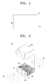
- FIGS. 1 and 2 A typical example of such an inverter power module for use in the electric/electronic device is illustrated in FIGS. 1 and 2 , and a construction thereof is briefly explained as follows.
- a general inverter power module 1 is configured, so that a power transformer 20, an inverter transformer 30 and a plurality of elements (not illustrated) are mounted on a driving circuit board 10.
- the inverter transformer 30 is provided with a bobbin 31 having a plurality of lead pins 31a connected to the driving circuit board 10, a first core 32 disposed in the bobbin 31, a coil 33 wound on the bobbin 31 and connected to the lead pins, and a cover 34 to accommodate the bobbin 31, the first core 32 and the coil 33.
- a magnetic flux is generated from the inverter transformer 30 as a single inverter transformer 30 drives a plurality of LCD lamps (not illustrated) in parallel. Such a magnetic flux is emitted to heat sinks (not illustrated) or shields (not illustrated) around the inverter power module 1.
- an electromagnetic interference (EMI) noise is greatly generated due to the emission of the magnetic flux to the outside.
- EMI noise exceeds a generally acceptable threshold (see one-dotted line in FIG. 3 ) by approximately 10dB (see dotted line in FIG. 3 ) in an area A due to the magnetic flux.
- an aspect of the present invention is to provide an inverter transformer, which blocks a magnetic flux that is generated from the inverter transformer from being emitted to the outside, thereby allowing an EMI noise, a heating problem, a noise of the system circuit, etc., to be minimized, and an inverter power module having the same for use in an electric/electronic device.
- an inverter power module for use in an electric/electronic device includes a driving circuit board, a power transformer mounted on the driving circuit board, an inverter transformer mounted on the driving circuit board, and a blocking unit to block a magnetic flux that is generated from the inverter transformer from being emitted to the outside.
- the inverter transformer may include a bobbin having a plurality of lead pins connected to the driving circuit board, a first core disposed in the bobbin, a coil wound on the bobbin and connected to the lead pins, and a cover to accommodate the bobbin, the first core and the coil.
- the blocking unit may include a first blocking unit to block the magnetic flux from being emitted above the inverter transformer.
- the first blocking unit comprises a second core detachably disposed to an upper surface of the cover.
- the second core is disposed side by side with respect to the first core.
- the second core has a horizontal area larger than that of the first core.
- the cover has an inserting groove formed in the upper surface thereof to insert the second core.
- the blocking unit further includes a second blocking unit to block the magnetic flux from being emitted below the inverter transformer.
- the second blocking unit comprises a third core detachably disposed with respect to a protection element installed below the driving circuit board to correspond to the inverter transformer.
- the third core is disposed side by side to the first and the second cores.
- the protection element has an inserting groove formed to insert the third core.
- the second core is detachably disposed on an upper surface of a cover.
- the cover has an inserting groove formed with respect to the upper surface thereof to insert the second core.
- FIG. 1 is a view schematically exemplifying a general inverter power module
- FIG. 2 is a perspective view of an inverter transformer illustrated in FIG. 1 ;
- FIG. 3 is a graph exemplifying the amount of EMI noise measured from the general inverter power module
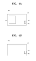
- FIGS. 4A and 4B are views schematically exemplifying an inverter power module according to an exemplary embodiment of the present invention.
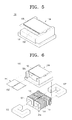
- FIG. 5 is a perspective view of an inverter transformer illustrated in FIG. 4A ;
- FIG. 6 is an exploded perspective view of the inverter transformer illustrated in FIG. 5 ;
- FIG. 7 is a perspective view of a protection element illustrated in FIG. 4B ;
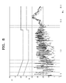
- FIG. 8 is a graph exemplifying the amount of EMI noise measured from the inverter power module according to an exemplary embodiment of the present invention.
- FIGS. 4A and 4B are views schematically exemplifying an inverter power module according to an exemplary embodiment of the present invention
- FIG. 5 is a perspective view of an inverter transformer illustrated in FIG. 4A
- FIG. 6 is an exploded perspective view of the inverter transformer illustrated in FIG. 5
- FIG. 7 is a perspective view of a protection element illustrated in FIG. 4B .
- the inverter power module 100 includes a driving circuit board 110, a power transformer 120, an inverter transformer 130 and a blocking unit, and uses a Hot output electric power as an input electric power of the inverter transformer 130.
- the driving circuit board 110 is configured in the form of one board, which drives a plurality of LCD lamps in parallel. As illustrated in FIG. 4A , on an upper surface of the driving circuit board 110 are mounted the power transformer 120, the inverter transformer 130, etc., and as illustrated in FIG. 4B , on a lower surface of the driving circuit board 110 are mounted a protection element 140, etc. On the upper and lower surfaces of the driving circuit board 110 are formed metal patterns (not illustrated), which electrically connect the respective elements mounted thereon.
- the inverter transformer 130 is provided with a bobbin 131 having a plurality of lead pins 131a connected to the driving circuit board 110, a first core 132 disposed in the bobbin 131, a coil 133 wound on the bobbin 131 and connected to the lead pins, and a cover 134 accommodating the bobbin 131, the first core 132 and the coil 133.
- an inserting groove 135a in which a second core 152 to be described later is inserted. It is preferable, but not necessary, that the inserting groove 135a is formed side by side or parallel to a longitudinal direction of the first core 132 and the coil 133.
- the blocking unit blocks a magnetic flux that is generated from the inverter transformer 130 from being emitted to the outside.
- the blocking unit is provided with a first blocking unit 150 to block the magnetic flux from being emitted above the inverter transformer 130, and a second blocking unit 160 to block the magnetic flux from being emitted below the inverter transformer 130.
- the first blocking unit 150 comprises a second core 152.
- the second core 152 is inserted in the inserting groove 135a formed in the upper surface 135 of the cover 134, so that it is detachably disposed on the upper surface of the cover 134.
- the second core 152 is a plate, which has a predetermined area, for example, a horizontal area larger than that of the first core 132, so as to cover upper parts of the first core 132 and the coil 133. It is preferable that the second core 152 has a thickness, which is inserted into the inserting groove 135a. It is preferable, but not necessary, that the second core 152 is constructed as at least one plate and disposed side by side to the first core 132.
- the second core 152 is shown comprising two plates. Also, it is preferable, but not necessary, that the second core 152 is formed of the same material as that of the first core 132. Although in the present embodiment, the second core 152 is illustrated as detachably installed to the cover 134, it can be also installed to mounting structures besides the cover 134.
- the second blocking unit 160 comprises a third core 162 disposed in a protection element 140 of insulating material.
- the protection element 140 is installed below the driving circuit board 110 to correspond to the inverter transformer 130. Since the protection element 140 is well-known in the art, detailed description thereof will be omitted.
- an inserting groove 140a which accommodates the third core 162 to be detachably installed therein.
- the third core 162 is constructed as at least one plate and disposed side by side to the first and the second cores 132 and 152. In this case, the third core 162 is shown comprising two plates. Also, it is preferable that the third core 162 is formed of the same material as that of the first and the second cores 132 and 152.
- the inverter power module 100 As a single inverter transformer 130 drives the plurality of LCD lamps in parallel, a magnetic flux is generated from the inverter transformer 130.
- the first and the second blocking units 150 and 160 for example, the second and the third cores 162, which are installed above and below the inverter transformer 130, respectively, block the magnetic flux generated from the inverter transformer 130 from being emitted to the outside.
- the second core 152 is inserted into the inserting groove 135a formed in the upper surface 135 of the cover 134 of the inverter transformer 130 mounted on the upper surface of the driving circuit board 110, so that it blocks the magnetic flux from being emitted above the inverter transformer 130.
- the third core 162 is inserted into the inserting groove 140a formed in the protection element 140 installed below the driving circuit board 110, so that it blocks the magnetic flux from being emitted below the inverter transformer 130.
- an EMI noise due to the magnetic flux is greatly reduced by approximately more than 20 dB (see an area B) when compared to the related art as shown in FIG. 3 , as the magnetic flux that is generated from the inverter transformer 130 of the driving circuit board 110 is blocked from being emitted to the outside.
- the inverter transformer and the inverter power module having the same block the magnetic flux that is generated from the inverter transformer from being emitted to the outside, thereby reducing the EMI noise due to the magnetic flux.
- the inverter transformer and the inverter power module having the same block the magnetic flux from being transmitted to the surrounding shields, so that the conventional problem of the increase of temperature due to the generation of heat can be addressed and thus the lifespan of the product can be extended.
Landscapes
- Engineering & Computer Science (AREA)
- Power Engineering (AREA)
- Physics & Mathematics (AREA)
- Electromagnetism (AREA)
- Thermal Sciences (AREA)
- Microelectronics & Electronic Packaging (AREA)
- Inverter Devices (AREA)
- Shielding Devices Or Components To Electric Or Magnetic Fields (AREA)
- Power Conversion In General (AREA)
Applications Claiming Priority (1)
| Application Number | Priority Date | Filing Date | Title |
|---|---|---|---|
| KR1020070008393A KR20080070377A (ko) | 2007-01-26 | 2007-01-26 | 인버터 트랜스포머 및 이를 구비한 전기/전자기기용 인버터파워 모듈 |
Publications (2)
| Publication Number | Publication Date |
|---|---|
| EP1950773A2 true EP1950773A2 (fr) | 2008-07-30 |
| EP1950773A3 EP1950773A3 (fr) | 2011-02-23 |
Family
ID=39232906
Family Applications (1)
| Application Number | Title | Priority Date | Filing Date |
|---|---|---|---|
| EP07119625A Withdrawn EP1950773A3 (fr) | 2007-01-26 | 2007-10-30 | Transformateur inverseur et module d'alimentation à inverseur équipé de celui-ci à utiliser dans un dispositif électrique/électronique |
Country Status (4)
| Country | Link |
|---|---|
| US (1) | US7746206B2 (fr) |
| EP (1) | EP1950773A3 (fr) |
| KR (1) | KR20080070377A (fr) |
| CN (1) | CN101231906B (fr) |
Cited By (12)
| Publication number | Priority date | Publication date | Assignee | Title |
|---|---|---|---|---|
| WO2011019712A1 (fr) * | 2009-08-10 | 2011-02-17 | Volterra Semiconductor Corporation | Bobine d'induction couplée à régulation améliorée de l'inductance de fuite |
| US7994888B2 (en) | 2009-12-21 | 2011-08-09 | Volterra Semiconductor Corporation | Multi-turn inductors |
| US8102233B2 (en) | 2009-08-10 | 2012-01-24 | Volterra Semiconductor Corporation | Coupled inductor with improved leakage inductance control |
| US8174348B2 (en) | 2009-12-21 | 2012-05-08 | Volterra Semiconductor Corporation | Two-phase coupled inductors which promote improved printed circuit board layout |
| US8294544B2 (en) | 2008-03-14 | 2012-10-23 | Volterra Semiconductor Corporation | Method for making magnetic components with M-phase coupling, and related inductor structures |
| EP2624261A1 (fr) * | 2012-01-31 | 2013-08-07 | Samsung Electronics Co., Ltd. | Inductor multi-utilisable avec slim appareil d'image ecran plat |
| US8674802B2 (en) | 2009-12-21 | 2014-03-18 | Volterra Semiconductor Corporation | Multi-turn inductors |
| US8847722B2 (en) | 2002-12-13 | 2014-09-30 | Volterra Semiconductor Corporation | Method for making magnetic components with N-phase coupling, and related inductor structures |
| US8975995B1 (en) | 2012-08-29 | 2015-03-10 | Volterra Semiconductor Corporation | Coupled inductors with leakage plates, and associated systems and methods |
| US9019063B2 (en) | 2009-08-10 | 2015-04-28 | Volterra Semiconductor Corporation | Coupled inductor with improved leakage inductance control |
| US9373438B1 (en) | 2011-11-22 | 2016-06-21 | Volterra Semiconductor LLC | Coupled inductor arrays and associated methods |
| US10128035B2 (en) | 2011-11-22 | 2018-11-13 | Volterra Semiconductor LLC | Coupled inductor arrays and associated methods |
Families Citing this family (2)
| Publication number | Priority date | Publication date | Assignee | Title |
|---|---|---|---|---|
| KR101503308B1 (ko) * | 2007-05-21 | 2015-03-18 | 엘지디스플레이 주식회사 | 액정표시장치 |
| JP5840669B2 (ja) * | 2013-12-17 | 2016-01-06 | 株式会社デンソー | 電力変換装置 |
Family Cites Families (9)
| Publication number | Priority date | Publication date | Assignee | Title |
|---|---|---|---|---|
| JPH01227410A (ja) * | 1988-03-08 | 1989-09-11 | Kijima:Kk | 小形トランス |
| JPH03171607A (ja) * | 1989-11-29 | 1991-07-25 | Tokyo Electric Co Ltd | インバータ用トランス |
| JPH09167708A (ja) * | 1995-12-15 | 1997-06-24 | Toko Inc | インバータトランス |
| JP2000124043A (ja) * | 1998-10-13 | 2000-04-28 | Toko Inc | インバータトランス |
| JP3906405B2 (ja) * | 2001-05-25 | 2007-04-18 | ミネベア株式会社 | インバータトランス |
| JP3906413B2 (ja) * | 2003-01-07 | 2007-04-18 | ミネベア株式会社 | インバータトランス |
| TWI228731B (en) * | 2003-04-01 | 2005-03-01 | Delta Electronics Inc | Inverter transformer and core structure thereof |
| WO2004109722A1 (fr) * | 2003-06-09 | 2004-12-16 | Minebea Co.,Ltd. | Transformateur a inverseur |
| KR100542566B1 (ko) * | 2003-08-04 | 2006-01-11 | 삼성전자주식회사 | 전기/전자 제품용 인버터 파워 모듈 |
-
2007
- 2007-01-26 KR KR1020070008393A patent/KR20080070377A/ko not_active Ceased
- 2007-06-29 US US11/770,770 patent/US7746206B2/en not_active Expired - Fee Related
- 2007-10-30 EP EP07119625A patent/EP1950773A3/fr not_active Withdrawn
- 2007-11-20 CN CN2007101928135A patent/CN101231906B/zh not_active Expired - Fee Related
Cited By (17)
| Publication number | Priority date | Publication date | Assignee | Title |
|---|---|---|---|---|
| US8847722B2 (en) | 2002-12-13 | 2014-09-30 | Volterra Semiconductor Corporation | Method for making magnetic components with N-phase coupling, and related inductor structures |
| US8294544B2 (en) | 2008-03-14 | 2012-10-23 | Volterra Semiconductor Corporation | Method for making magnetic components with M-phase coupling, and related inductor structures |
| US9019063B2 (en) | 2009-08-10 | 2015-04-28 | Volterra Semiconductor Corporation | Coupled inductor with improved leakage inductance control |
| WO2011019712A1 (fr) * | 2009-08-10 | 2011-02-17 | Volterra Semiconductor Corporation | Bobine d'induction couplée à régulation améliorée de l'inductance de fuite |
| US8237530B2 (en) | 2009-08-10 | 2012-08-07 | Volterra Semiconductor Corporation | Coupled inductor with improved leakage inductance control |
| US8102233B2 (en) | 2009-08-10 | 2012-01-24 | Volterra Semiconductor Corporation | Coupled inductor with improved leakage inductance control |
| US8362867B2 (en) | 2009-12-21 | 2013-01-29 | Volterra Semicanductor Corporation | Multi-turn inductors |
| US8674802B2 (en) | 2009-12-21 | 2014-03-18 | Volterra Semiconductor Corporation | Multi-turn inductors |
| US7994888B2 (en) | 2009-12-21 | 2011-08-09 | Volterra Semiconductor Corporation | Multi-turn inductors |
| US8890644B2 (en) | 2009-12-21 | 2014-11-18 | Volterra Semiconductor LLC | Two-phase coupled inductors which promote improved printed circuit board layout |
| US8174348B2 (en) | 2009-12-21 | 2012-05-08 | Volterra Semiconductor Corporation | Two-phase coupled inductors which promote improved printed circuit board layout |
| US9281115B2 (en) | 2009-12-21 | 2016-03-08 | Volterra Semiconductor LLC | Multi-turn inductors |
| US9373438B1 (en) | 2011-11-22 | 2016-06-21 | Volterra Semiconductor LLC | Coupled inductor arrays and associated methods |
| US10128035B2 (en) | 2011-11-22 | 2018-11-13 | Volterra Semiconductor LLC | Coupled inductor arrays and associated methods |
| EP2624261A1 (fr) * | 2012-01-31 | 2013-08-07 | Samsung Electronics Co., Ltd. | Inductor multi-utilisable avec slim appareil d'image ecran plat |
| US8975995B1 (en) | 2012-08-29 | 2015-03-10 | Volterra Semiconductor Corporation | Coupled inductors with leakage plates, and associated systems and methods |
| US9721719B1 (en) | 2012-08-29 | 2017-08-01 | Volterra Semiconductor LLC | Coupled inductors with leakage plates, and associated systems and methods |
Also Published As
| Publication number | Publication date |
|---|---|
| CN101231906B (zh) | 2012-09-05 |
| US20080180207A1 (en) | 2008-07-31 |
| KR20080070377A (ko) | 2008-07-30 |
| EP1950773A3 (fr) | 2011-02-23 |
| US7746206B2 (en) | 2010-06-29 |
| CN101231906A (zh) | 2008-07-30 |
Similar Documents
| Publication | Publication Date | Title |
|---|---|---|
| US7746206B2 (en) | Inverter transformer and inverter power module having the same for use in electric/electronic device | |
| US7808572B2 (en) | Liquid crystal display device including heat conducting pads between shield cover and inverter IC and transformer | |
| CN101082715A (zh) | 用于液晶显示器件的逆变器以及使用其的液晶显示模块 | |
| US8953339B2 (en) | Power module and display device | |
| JP4616217B2 (ja) | トランスを含む液晶表示装置 | |
| US8284342B2 (en) | Liquid crystal display device and backlight device thereof | |
| KR20130025202A (ko) | 표시장치 | |
| KR101018220B1 (ko) | 파워 모듈 및 디스플레이 장치 | |
| KR101220020B1 (ko) | 백라이트 유닛 및 이를 구비한 표시 장치 | |
| EP3579218B1 (fr) | Unité de commande de dispositif d'affichage et dispositif d'affichage | |
| JP7488280B2 (ja) | 圧縮機の電子制御装置、圧縮機および冷却装置 | |
| KR20080069806A (ko) | 인버터 회로 기판 및 이를 포함하는 백 라이트 어셈블리 | |
| KR101065491B1 (ko) | 트랜스포머 | |
| KR20110120188A (ko) | 액정표시장치용 인버터 트랜스포머 | |
| WO2021017865A1 (fr) | Pcba et appareil de cuisson à flamme électrique | |
| KR200416466Y1 (ko) | 캡코어를 구비한 트랜스포머 | |
| KR20050051913A (ko) | 액정표시장치 | |
| JP2018082028A (ja) | 電源装置 | |
| JP3370054B2 (ja) | 遊技機用液晶表示装置 | |
| KR20110127549A (ko) | 백라이트 유닛 | |
| KR20080027739A (ko) | 액정 표시 장치 | |
| JP2004342997A (ja) | ケース付き回路基板、冷陰極管制御回路、およびケース付き回路基板の製造方法 | |
| KR101254804B1 (ko) | 트랜스포머 및 이를 포함하는 액정표시장치 | |
| JP2010225531A (ja) | 照明装置、表示装置、及びテレビ受信装置 | |
| KR100683747B1 (ko) | 플라즈마 디스플레이 장치 |
Legal Events
| Date | Code | Title | Description |
|---|---|---|---|
| PUAI | Public reference made under article 153(3) epc to a published international application that has entered the european phase |
Free format text: ORIGINAL CODE: 0009012 |
|
| AK | Designated contracting states |
Kind code of ref document: A2 Designated state(s): AT BE BG CH CY CZ DE DK EE ES FI FR GB GR HU IE IS IT LI LT LU LV MC MT NL PL PT RO SE SI SK TR |
|
| AX | Request for extension of the european patent |
Extension state: AL BA HR MK RS |
|
| PUAL | Search report despatched |
Free format text: ORIGINAL CODE: 0009013 |
|
| AK | Designated contracting states |
Kind code of ref document: A3 Designated state(s): AT BE BG CH CY CZ DE DK EE ES FI FR GB GR HU IE IS IT LI LT LU LV MC MT NL PL PT RO SE SI SK TR |
|
| AX | Request for extension of the european patent |
Extension state: AL BA HR MK RS |
|
| 17P | Request for examination filed |
Effective date: 20110823 |
|
| AKX | Designation fees paid |
Designated state(s): DE GB NL |
|
| 17Q | First examination report despatched |
Effective date: 20120523 |
|
| RAP1 | Party data changed (applicant data changed or rights of an application transferred) |
Owner name: SAMSUNG ELECTRONICS CO., LTD. |
|
| RIC1 | Information provided on ipc code assigned before grant |
Ipc: H02M 7/00 20060101AFI20130228BHEP Ipc: H05B 41/282 20060101ALI20130228BHEP Ipc: H01F 38/10 20060101ALI20130228BHEP Ipc: H01F 27/36 20060101ALI20130228BHEP |
|
| GRAP | Despatch of communication of intention to grant a patent |
Free format text: ORIGINAL CODE: EPIDOSNIGR1 |
|
| INTG | Intention to grant announced |
Effective date: 20130426 |
|
| RIN1 | Information on inventor provided before grant (corrected) |
Inventor name: PARK, CHEOL-JIN |
|
| STAA | Information on the status of an ep patent application or granted ep patent |
Free format text: STATUS: THE APPLICATION IS DEEMED TO BE WITHDRAWN |
|
| 18D | Application deemed to be withdrawn |
Effective date: 20130907 |