EP1962229A2 - Étiquette RFID et procédé de fabrication d'étiquette RFID - Google Patents
Étiquette RFID et procédé de fabrication d'étiquette RFID Download PDFInfo
- Publication number
- EP1962229A2 EP1962229A2 EP07124106A EP07124106A EP1962229A2 EP 1962229 A2 EP1962229 A2 EP 1962229A2 EP 07124106 A EP07124106 A EP 07124106A EP 07124106 A EP07124106 A EP 07124106A EP 1962229 A2 EP1962229 A2 EP 1962229A2
- Authority
- EP
- European Patent Office
- Prior art keywords
- circuit
- chip
- circuit chip
- terminals
- pad
- Prior art date
- Legal status (The legal status is an assumption and is not a legal conclusion. Google has not performed a legal analysis and makes no representation as to the accuracy of the status listed.)
- Granted
Links
Images


Classifications
-
- G—PHYSICS
- G06—COMPUTING OR CALCULATING; COUNTING
- G06K—GRAPHICAL DATA READING; PRESENTATION OF DATA; RECORD CARRIERS; HANDLING RECORD CARRIERS
- G06K19/00—Record carriers for use with machines and with at least a part designed to carry digital markings
- G06K19/06—Record carriers for use with machines and with at least a part designed to carry digital markings characterised by the kind of the digital marking, e.g. shape, nature, code
- G06K19/067—Record carriers with conductive marks, printed circuits or semiconductor circuit elements, e.g. credit or identity cards also with resonating or responding marks without active components
- G06K19/07—Record carriers with conductive marks, printed circuits or semiconductor circuit elements, e.g. credit or identity cards also with resonating or responding marks without active components with integrated circuit chips
- G06K19/077—Constructional details, e.g. mounting of circuits in the carrier
- G06K19/07749—Constructional details, e.g. mounting of circuits in the carrier the record carrier being capable of non-contact communication, e.g. constructional details of the antenna of a non-contact smart card
-
- G—PHYSICS
- G06—COMPUTING OR CALCULATING; COUNTING
- G06K—GRAPHICAL DATA READING; PRESENTATION OF DATA; RECORD CARRIERS; HANDLING RECORD CARRIERS
- G06K19/00—Record carriers for use with machines and with at least a part designed to carry digital markings
- G06K19/06—Record carriers for use with machines and with at least a part designed to carry digital markings characterised by the kind of the digital marking, e.g. shape, nature, code
- G06K19/067—Record carriers with conductive marks, printed circuits or semiconductor circuit elements, e.g. credit or identity cards also with resonating or responding marks without active components
- G06K19/07—Record carriers with conductive marks, printed circuits or semiconductor circuit elements, e.g. credit or identity cards also with resonating or responding marks without active components with integrated circuit chips
- G06K19/077—Constructional details, e.g. mounting of circuits in the carrier
- G06K19/07749—Constructional details, e.g. mounting of circuits in the carrier the record carrier being capable of non-contact communication, e.g. constructional details of the antenna of a non-contact smart card
- G06K19/0775—Constructional details, e.g. mounting of circuits in the carrier the record carrier being capable of non-contact communication, e.g. constructional details of the antenna of a non-contact smart card arrangements for connecting the integrated circuit to the antenna
-
- H—ELECTRICITY
- H10—SEMICONDUCTOR DEVICES; ELECTRIC SOLID-STATE DEVICES NOT OTHERWISE PROVIDED FOR
- H10P—GENERIC PROCESSES OR APPARATUS FOR THE MANUFACTURE OR TREATMENT OF DEVICES COVERED BY CLASS H10
- H10P72/00—Handling or holding of wafers, substrates or devices during manufacture or treatment thereof
- H10P72/70—Handling or holding of wafers, substrates or devices during manufacture or treatment thereof for supporting or gripping
- H10P72/74—Handling or holding of wafers, substrates or devices during manufacture or treatment thereof for supporting or gripping using temporarily an auxiliary support
- H10P72/7428—Handling or holding of wafers, substrates or devices during manufacture or treatment thereof for supporting or gripping using temporarily an auxiliary support used to support diced chips prior to mounting
-
- H—ELECTRICITY
- H10—SEMICONDUCTOR DEVICES; ELECTRIC SOLID-STATE DEVICES NOT OTHERWISE PROVIDED FOR
- H10W—GENERIC PACKAGES, INTERCONNECTIONS, CONNECTORS OR OTHER CONSTRUCTIONAL DETAILS OF DEVICES COVERED BY CLASS H10
- H10W72/00—Interconnections or connectors in packages
- H10W72/01—Manufacture or treatment
- H10W72/0198—Manufacture or treatment batch processes
-
- H—ELECTRICITY
- H10—SEMICONDUCTOR DEVICES; ELECTRIC SOLID-STATE DEVICES NOT OTHERWISE PROVIDED FOR
- H10W—GENERIC PACKAGES, INTERCONNECTIONS, CONNECTORS OR OTHER CONSTRUCTIONAL DETAILS OF DEVICES COVERED BY CLASS H10
- H10W72/00—Interconnections or connectors in packages
- H10W72/071—Connecting or disconnecting
- H10W72/072—Connecting or disconnecting of bump connectors
- H10W72/07251—Connecting or disconnecting of bump connectors characterised by changes in properties of the bump connectors during connecting
-
- H—ELECTRICITY
- H10—SEMICONDUCTOR DEVICES; ELECTRIC SOLID-STATE DEVICES NOT OTHERWISE PROVIDED FOR
- H10W—GENERIC PACKAGES, INTERCONNECTIONS, CONNECTORS OR OTHER CONSTRUCTIONAL DETAILS OF DEVICES COVERED BY CLASS H10
- H10W72/00—Interconnections or connectors in packages
- H10W72/20—Bump connectors, e.g. solder bumps or copper pillars; Dummy bumps; Thermal bumps
-
- H—ELECTRICITY
- H10—SEMICONDUCTOR DEVICES; ELECTRIC SOLID-STATE DEVICES NOT OTHERWISE PROVIDED FOR
- H10W—GENERIC PACKAGES, INTERCONNECTIONS, CONNECTORS OR OTHER CONSTRUCTIONAL DETAILS OF DEVICES COVERED BY CLASS H10
- H10W90/00—Package configurations
- H10W90/701—Package configurations characterised by the relative positions of pads or connectors relative to package parts
- H10W90/721—Package configurations characterised by the relative positions of pads or connectors relative to package parts of bump connectors
- H10W90/724—Package configurations characterised by the relative positions of pads or connectors relative to package parts of bump connectors between a chip and a stacked insulating package substrate, interposer or RDL
Definitions
- the present invention relates to an RFID (Radio Frequency IDentification) tag which exchanges information with external equipment in a non-contact manner and relates to its manufacturing method.
- RFID Radio Frequency IDentification
- the "RFID tag” used in the present specification is also called as an "RFID tag inlay” among those skilled in the art, meaning an internal constituent part (inlay) used in the "RFID tag”.
- the "RFID tags” include a contactless IC card.
- RFID tag As a type of RFID tag, there has been proposed a configuration in which an antenna pattern for wireless communications and an IC chip are mounted on a base sheet made of plastics or paper.
- One possible application for RFID tags of this type is to affix them to goods and identify the goods by exchanging information about the goods with external equipment.
- Fig. 1 is a schematic cross-sectional view showing an example of RFID tags of this type.
- An RFID tag 10 shown here has an antenna 12 formed of a conductive pattern on a sheet type base 11 and a circuit chip 13 mounted thereon. A circuit for exchanging information with external equipment via the antenna 12 is incorporated into the circuit chip 13. Connection terminals 13a formed on the lower surface of the circuit chip 13 are electrically connected to two mounting pads of the antenna 12 (to be described later), which are formed to be close to each other, by soldering or the like, and each of their surroundings is fixed to the base 11 with an adhesive 14.
- connection terminals of the circuit chip is one condition that contributes to allowing mass production to reduce the cost of products.
- connection terminals are arranged in such a way that the circuit chip must be directed in a specific direction to be electrically connected to antenna terminals, postures of the circuit chip must be precisely controlled one by one at the time of connection. This may be an impediment to improvement in productivity.
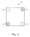
- Fig. 2 is a diagram showing a first example of connection terminals formed on the lower surface of the circuit chip.
- Fig. 2 shows a square circuit chip 13A. At four corners of the lower surface of the square circuit chip 13A, each of four terminals in total is formed, which is connected to one of two mounting pads 121 and 122 (see Fig. 3 ) to be described later.
- two terminals 131 of one diagonal are antenna terminals that are connected to an electronic circuit in the circuit chip 13A to provide an electrical connection to an antenna 12 (see Fig. 1 ).
- the other two terminals of the other diagonal are dummy terminals that are non-connected to the electronic circuit in the circuit chip 13A and that aim to improve stabilization of the posture of the circuit chip 13A when the circuit chip 13A is mounted.
- Fig. 3 is a diagram showing a positional relationship between the mounting pads and the circuit chip.
- FIG. 3 shows two mounting pads 121 and 122, these two mounting pads 121 and 122 correspond to two end sections of the antenna 12 shown in Fig. 1 , which are positioned at the circuit chip 13 sides and arranged close to each other.
- the circuit chip 13A may be disposed in a positional relationship with respect to the mounting pads 121and 122 as shown in Fig. 3 , and may be rotated about a central point O of the circuit chip 13A by any angle of 90 degrees, 180 degrees and 270 degrees in the direction of an arrow from the positional relationship shown in Fig. 3 .
- one of two antenna terminals 131 and 132 is connected to one of two mounting pads 121 and 122, and the other antenna is connected to the other mounting pad. Accordingly, even when the circuit chip is connected to the mounting pad at any rotation position, the normal operation as the RFID tag can be expected.
- this terminal arrangement eliminates the need for considering the direction of the circuit chip in mounting the circuit chip on the mounting pads, and is expected to simplify mounting equipment and achieve high-speed mounting.
- the antenna terminals 131 of one diagonal and the dummy terminals 132 of the other diagonal cannot be always arranged as shown in Fig. 2 .
- the terminals may be arranged as shown in Fig. 4 to be explained below.
- Fig. 4 is a diagram showing a second example of a terminal arrangement of the lower surface of the circuit chip.
- Fig. 4 shows a square circuit chip 13B, however, the terminal arrangement differs from that of the circuit chip 13A in Fig. 13A . Specifically, each of four terminals in total is formed at one of four corners of the lower surface of the circuit chip 13B. However, among the four terminals, each of two antennas terminals 131 in total is formed at one of two corners along one side 139 of the lower surface of the circuit chip 13B and the remaining two terminals are formed as dummy terminals 132.
- the circuit chip 13b having this terminal arrangement is assumed to be rotated by 90 degrees, 180 degrees and 270 degrees.
- Fig. 5 is a diagram showing the positional relationship between the mounting pads and the circuit chip 13B having the terminal arrangement shown in Fig. 4 .
- Part (A) of Fig. 5 shows a state in which the circuit chip 13B shown in Fig. 4 is formed on the mounting pads 121 and 122 with the posture shown in Fig. 4 unchanged.
- a state is shown in which the circuit chip 13B is rotated about a central point O of the circuit chip 13B by each of 90 degrees, 180 degrees and 270 degrees in the direction of an arrow from the posture shown in part (A) of Fig. 5 .
- Fig. 6 is a diagram showing a terminal arrangement of a circuit chip proposed in Japanese Patent Application Publication No. 2005-107882 .
- a circuit 13C shown in Fig. 6 also has a square shape, however, dummy terminals are not formed unlike those shown in Figs. 2 and 4 , and all of four terminals formed at four corners are antenna terminals connected to the internal circuit. It is noted that two antenna terminals 131a formed at two corners along one side 139a of the lower surface of the circuit chip 13C are connected to each other on the internal circuit, while two antenna terminals 131b formed at two corners along another one side 139b are also connected to each other on the internal circuit.
- Fig. 7 is a diagram showing a state in which a circuit chip having the terminal arrangement shown in Fig. 6 is formed on mounting pads each having a shape proposed in Japanese Patent Application Publication No. 2005-107882 .
- Pads 121' and 122' shown in Fig. 7 are shaped to be connected to only any one of four terminals formed at four corners of the circuit chip 13C.
- Part (A) of Fig. 7 shows a state in which the circuit chip 13C shown in Fig. 6 is formed on the mounting pads 121' and 122' with the posture shown in Fig. 6 unchanged.
- a state is shown in which the circuit chip 13C is rotated about a central point O of the circuit chip 13C by each of 90 degrees, 180 degrees and 270 degrees in the direction of an arrow from the posture shown in part (A) in Fig. 7 .
- circuit chip 13C having the terminal arrangement shown in Fig. 6 and the mounting pads 121' and 122' each having a shape shown in Fig. 7 , one and the other mounting pads 121' and 122' are formed on one and the other antenna terminals 131a and 131b, respectively, regardless of the rotation state of the circuit chip 13C. Therefore, it is possible to connect the circuit chip 13C to the mounting pads 121' and 122' without considering the rotation of the circuit chip 13C, which is expected to simplify mounting equipment and achieve high-speed mounting.
- circuit chip 13C shown in Fig. 6 although two terminals each are electrically connected to each other in the internal circuit, such connection originally allows the use of only terminals of one diagonal as antenna terminals and terminals of the other diagonal as dummy terminals as shown in Fig. 2 .
- all four terminals formed at four corners are used for connection without considering the rotation position of the circuit chip as shown in Fig. 3 , which makes it possible to improve stabilization of the circuit chip when the circuit chip is mounted, and therefore there are no merits in the configurations as in Figs. 6 and 7 .
- the present invention has been made in view of the above circumstances and provides an RFID tag in which a circuit chip is used when two terminals along one side are terminal antennas and the remaining two terminals are dummy terminals as shown in Fig. 4 and the circuit chip is mounted using all four terminals regardless of a rotation position thereof, and provides a manufacturing method of the RFID tag suitable for mass production.
- An RFID tag of the present invention includes: a base; a communication antenna which is wired on the base and has two mounting pads close to each other; and a square circuit chip mounted on the base and electrically connected to the mounting pads to perform radio communications via the mounted antenna, wherein:
- a first pad of two mounting pads is composed of first and second sub-pads connected to two terminals formed at two positions on one diagonal of a lower surface of a circuit chip, respectively, and a second pad is composed of third and fourth sub-pads connected to two terminals formed at two positions on the other diagonal of the lower surface of the circuit chip, respectively. Therefore, even when employing the circuit chip having the terminal arrangement shown in Fig. 4 where the terminals formed at two corners along one side of the lower surface of the circuit chip are antenna terminals and two terminals except for these antenna terminals are dummy terminals, it is possible to mount the circuit chip using all four terminals without considering the rotation state, which makes it possible to simplify mounting equipment and achieve high-speed mounting.
- each of the third sub-pad and the fourth sub-pad has an adding section expanding to a central position of the lower surface of the mounted circuit chip, so that a total area of the first sub-pad, the second sub-pad and the connection section becomes equal to a total area of the third sub-pad and the fourth sub-pad in terms of region overlapping with the mounted circuit chip.
- edge lines of each of regions of the first, second, third, and fourth sub-pads overlapping with the mounted circuit chip except for the connection section and the adding sections extend in parallel to each other or perpendicularly to each other, while the connection section and the adding sections are formed in regions overlapping with the mounted circuit chip.
- an RFID tag manufacturing method of manufacturing an RFID tag which has a base, a communication antenna having two mounting pads close to each other and wired on the base, and a square circuit chip mounted on the base and electrically connected to the mounting pads to perform radio communications via the antenna, includes:
- antenna wiring patterns are two-dimensionally arrayed on the web and the circuit chips are transferred on the web to be connected, thereby the RFID tags can be efficiently mass-produced.
- the rotation state of the circuit chips cannot be controlled in aligning the circuit chips on the alignment mask, but there is no need to control the rotation state of the circuit chips of the RFID tags according to the manufacturing method of the present invention.
- This manufacturing method allows high efficient production by use of the point that there is no need to control the rotation state of the circuit chip.
- the chip alignment step may be a step of aligning the plurality of circuit chips on the alignment mask while a lower surface of each of the circuit chips on which surface terminals are arrayed is directed downward, and
- the chip transfer step may be a step of placing an adhesive support member on upper surfaces of the circuit chips aligned on the alignment mask to transfer the circuit chips onto the support member at one time, and transferring the circuit chips transferred to the support member onto the web at one time.
- the chip alignment step may be a step of aligning the plurality of circuit chips on the alignment mask while a lower surface of each of the circuit chips on which surface terminals are arrayed is directed downward
- the chip transfer step may be a step of transferring, at one time, the circuit chips aligned on the alignment mask onto a downward-facing surface of the web on which surface the wiring patterns are formed.
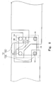
- Fig. 8 is an enlarged view of a circuit chip mounting section of an RFID tag according to a first embodiment of the present invention.
- This figure shows the same circuit chip 13B as that shown in Fig. 4 .
- the circuit chip 13B is square shaped, and has respective terminals at four corners of the lower surface of the circuit chip 13B.
- two terminals which are formed at two corners along one side 139, respectively, are antenna terminals 131 that connect a circuit mounted on the circuit chip 13B to an antenna.
- Remaining two terminals except for the two antenna terminals 131 are dummy terminals 132 that are non-connected to the circuit mounted on the circuit chip 13B, and that aim to improve stabilization of the posture of the circuit chip 13B when it is mounted.
- the circuit 13B is mounted in a mounting region enclosed by an alternate long and short dashed line.
- the mounting region has: a first mounting pad 121 which is composed of a first sub-pad 121a, a second sub-pad 121b and a connection section 121c; and a second mounting pad 122 which is composed of a third sub-pad 122a and a fourth sub-pad 122b.
- the first sub-pad 121a and the second sub-pad 121b of the first mounting pad 121 are connected to two terminals of one diagonal formed on the lower surface of the circuit chip 13B, respectively.
- the connection section 121c extends in a manner overlapping with the mounted circuit chip 13B, and connects the first sub-pad 121a to the second sub-pad 121b.
- the third sub-pad 122a and the fourth sub-pad 122b of the second mounting pad 122 are connected to two terminals of the other diagonal formed on the lower surface of the circuit chip 13B, respectively.
- the third sub-pad 122a and the fourth sub-pad 122b are connected to each other via a route that bypasses the mounted circuit chip 13B.
- the dummy terminal 132 is connected to the first sub-pad 121a, the antenna terminal 131 is connected to the second sub-pad 121b, the dummy terminal 132 is connected to the third sub-pad 122a, and the antenna terminal 131 is connected to the fourth sub-pad 122b.
- one antenna terminal 131 is connected to the first mounting pad 121, and another antenna terminal 131 is connected to the second mounting pad 122.
- the RFID tag under this connection state operates normally.
- Figs. 9 , 10 and 11 are diagrams each showing a state in which the circuit chip 13B shown in Fig. 8 is rotated by each of 90 degrees, 180 degrees and 270 degrees to be mounted on the mounting pads.
- the antenna terminal 131, the dummy terminal 132, the dummy terminal 132, and the antenna terminal 131 are connected to the first sub-pad 121a, the second sub-pad 121b, the third sub-pad 122a, and the fourth sub-pad 122b, respectively. Accordingly, the antenna terminals 131 are connected to both the first mounting pad 121 and the second mounting pad 122, respectively, in which case the RFID tag also operates normally.
- the antenna terminal 131, the dummy terminal 132, the antenna terminal 131, and the dummy terminal 132 are connected to the first sub-pad 121a, the second sub-pad 121b, the third sub-pad 122a, and the fourth sub-pad 122b, respectively. Accordingly, the antenna terminals 131 are connected to both the first mounting pad 121 and the second mounting pad 122, respectively, in which case the RFID tag also operates normally.
- the dummy terminal 132, the antenna terminal 131, the antenna terminal 131, and the dummy terminal 132 are connected to the first sub-pad 121a, the second sub-pad 121b, the third sub-pad 122a, and the fourth sub-pad 122b, respectively.
- the antenna terminals 131 are connected to both the first mounting pad 121 and the second mounting pad 122, respectively, in which case the normal operation of the RFID tag can be also expected.
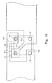
- Fig. 12 is an enlarged view of a circuit chip mounting section of an RFID tag according to a second embodiment of the present invention.
- Fig. 12 differs from Fig. 8 in the way of drawing the figure, for the purpose of explaining the adding sections 1222a and 1222b, and the difference in the RFID tag therebetween is only the presence or absence of the adding sections 1222a and 1222b.
- an overlapped region 1211a of the first sub-pad 121a with the mounted circuit chip 13B an overlapped region 1211b of the second sub-pad 121b with the mounted circuit chip 13B, an overlapped region 1221a of the third sub-pad 122a with the mounted circuit chip 13B, an overlapped region 1221b of the fourth sub-pad 122b with the mounted circuit chip 13B, its edge lines extend in parallel or perpendicularly (for example, vertical and horizontal lines each having a length "e" regarding the overlapped region 1221b, the same is applied to other overlapped regions 1221a, 1211a, 1211b) .
- each of these four regions 1211a, 1211b, 1221a, and 1221b has an area, "e x e", as a design central value with no consideration of the positional shift of the circuit chip 13B when it is mounted.
- the positional shift of the circuit chip 13B when it is mounted will be described later.
- each of the two adding sections 1222a and 1222b is decided such that an area of the connection section 121c and a total area of the two adding sections 1222a and 1222b are equal to each other. Specifically, in this embodiment, each of the two adding sections 1222a and 1222b has an area equal to a half of that of the connection section 121c.
- the total area of the overlapped region 1211a of the first sub-pad 121a with the mounted circuit chip 13B, the overlapped region 1211b of the second sub-pad 121b with the mounted circuit chip 13B and the connection section 121c becomes equal to the total area of the overlapped region 1221a and 1222a of the third sub-pad 122a with the mounted circuit chip 13B and the overlapped region 1221b and 1222b of the fourth sub-pad 122b with the mounted circuit chip 13B.
- Fig. 13 is a diagram of an RFID tag according to a second embodiment of the present invention shown in Fig. 12 to indicate a state in which the circuit chip is mounted at a standard position as in a design value.
- Fig. 14 is a diagram of the RFID according to the second embodiment of the present invention shown in Fig. 12 to indicate a state in which the circuit chip is mounted at a position shifted horizontally by ⁇ as compared with the standard position shown in Fig. 13 .
- circuit chip 13B has a square shape, and its contour line extends in up and down directions or left and right directions. Moreover, all the edge lines, of the respective overlapped regions 1211a, 1211b, 1221a and 1221b with the circuit chip 13B formed on the respective pads, also extend in up and down directions or left and right directions.
- the circuit chip 13B is horizontally shifted by the mounting shift length ⁇ , so that the area of the overlapped region 1211a of the first sub-pad is increased by " ⁇ ⁇ e", and the area of the overlapped region 1211b of the second sub-pad is decreased by " ⁇ ⁇ e".
- the area of the overlapped region of the first mounting pad with the circuit chip 13B -- which first mounting pad is composed of the first sub-pad, the second sub-pad, and the connection section 121c -- is maintained constant regardless of the length of the mounting shift " ⁇ ".
- Fig. 14 shows the state in which the circuit chip 13B is shifted in the left direction in Fig. 14 to be mounted. However, even if the circuit chip 13B is shifted in the right direction in Fig.
- the area of the overlapped region of the first mounting pad with the circuit chip 13B, and the area of the overlapped region of the second mounting pad with the circuit chip 13B are maintained constant. Moreover, even if the circuit chip 13B is shifted in the upward or downward direction in Fig. 14 to be mounted, the same result is obtained.
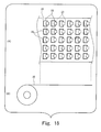
- Fig. 15 is a diagram showing a web serving as a base of the RFID tag after cutting (see the base 11 in Fig. 1 ).
- a web 20 shown in Fig. 15 is rolled as shown in part (B) of Fig. 15 .
- Part (A) of Fig. 15 is an enlarged plan view of a part of the web 20, and multiple wiring patterns 22 functioning as an antenna (see the antenna 12 in Fig. 1 ) are two-dimensionally arrayed on the web 20 with a fixed pitch after the RFID tag is manufactured.
- chip mounting regions 23 are each indicated by a broken line.
- Fig. 16 is a plan view of an alignment mask
- Fig. 17 is a cross-sectional view taken along line A-A' of Fig. 16 .
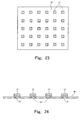
- the number of chip alignment holes 31 formed on an alignment mask 30 is reduced and shown in an enlarged manner.
- Fig. 18 is a diagram showing a state in which circuit chips are aligned on the alignment mask shown in Figs. 16 and 17 .
- the alignment mask 30 there are the two-dimensionally arrayed chip alignment holes 31 in which the circuit chips 13 are inserted as shown in Fig. 18 .
- the array pitch of the chip alignment holes 31 is the same as that of the wiring patterns 22 on the web 20 shown in Fig. 15 .
- Each chip alignment hole 31 has a taper shape that has a surface with a wide opening and becomes gradually narrower towards the rear face side in order to align the circuit chips 13 smoothly.
- the positional accuracy of the alignment of the circuit chips 13 depends on the accuracy of the array of chip alignment holes 31.
- a thin stainless steel plate or metallic plate made of a material such as aluminum is used as the alignment mask 30, and the chip alignment holes 31 are formed by etching.
- the chip alignment holes 31 can be formed with sufficiently high positional accuracy by etching.
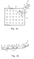
- Figs. 19 and 20 are a plan view and a cross-sectional view each showing a state of supply of circuit chips onto the alignment mask.
- a chip supply jig 40 having a frame 41 is attached to the alignment mask 30 to prevent the circuits chips 13 supplied onto the alignment mask 30 from dropping.
- the chip supply jig 40 is inclined as a whole as shown in Fig. 20 to supply the same number of circuit chips 13 as that of the alignment holes 31 formed on the alignment mask 30.
- the circuit chips 13 are supplied in a state that the terminal 13a (see the terminal 13a in Fig. 1 ) connected to the antenna is directed downward.
- a soldering ball (not shown) for soldering later is fixed onto the terminal 13a of the circuit chip 13.
- Figs. 21 and 23 are a plan view and a cross-sectional view each showing a state in which the circuit chips are aligned after the necessary number of circuit chips are supplied onto the alignment mask.
- Figs. 23 and 24 are a plan view and a cross-sectional view each showing a state in which the circuit chips are aligned on the alignment mask.
- the entirety of the alignment mask 30 is next oscillated or inclined in various directions as illustrated by arrows in Figs. 21 and 22 to insert the circuit chips 13 into the chip alignment holes 31 one by one to thereby align the circuit chips 13 as shown in Figs. 23 and 24 .
- Fig. 25 is a diagram showing a state in which an adhesive film is pressed onto the circuit chips on the alignment mask
- Fig. 26 is a diagram showing a state in which the circuit chips on the alignment mask are adhered onto the adhesive film and the result is lifted.
- Fig. 27 is a diagram showing a web to which adhesive is supplied.
- the circuit chips aligned on the alignment mask 30 are supplied onto the web 20 at one time after being lifted at one time as shown in Figs. 25 and 26 .
- an adhesive 24 is coated or disposed by printing on the regions 23 of the web 20 where the circuit chips are to be mounted as shown in Fig. 27 .
- Figs. 28 to 30 are diagrams each showing a state in which the circuit chips lifted from the alignment mask 30 at one time as shown in Fig. 26 are supplied onto the web at one time.
- a section of the web 20 where the circuit chips 13 are to be supplied is placed on a stage 53, the circuit chips 13 are conveyed to a position above the stage 53 such that the circuit chips 13 are aligned to be correctly overlapped with the chip mounting regions 23 on the web 20 (see Figs. 15 and 27 ) as shown in Fig. 28 , and the circuit chips 13 are pressed onto the web 20 at one time as shown in Fig. 29 .
- the adhesive film 51 is lifted as shown in Fig. 30
- the circuit chips 13 remain mounted on the web 20.
- the adhesive 24 to be supplied onto the web 20 there is used an adhesive having adhesion sufficiently stronger than that of the adhesive film 51 to prevent the circuit chips 13 from being lifted by being adhered to the adhesive film 51, and to prevent the positions of the circuit chips 13 from being shifted when the adhesive film 51 is lifted.
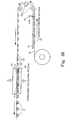
- Fig. 31 is a diagram showing a more reliable method for mounting circuit chips onto the web.
- a press plate having pin insertion holes 521 with the same array pitch as that of the circuit chip 13 is used here as the press plate 52.
- press pins 551 of a press pin mechanism 55 which are arranged with the same pitch as that of the pin insertion holes 521 of the press plate 52, are inserted into the pin insertion holes 521, and the adhesive film 51 is lifted while the circuit chips 13 are pressed from above. In this way, it is possible to mount the circuit chips 13 on the web 20 more reliably.
- Fig. 32 is a diagram showing a state of mounting the circuit chips 13 supplied on the web 20
- Fig. 33 is a diagram showing the web 20 in a state that the mounting of the circuit chips 13 is completed.
- the soldering ball (not shown) is fixed onto the terminal 13a of the circuit chip 13.
- a pressuring and heating head 56 is pressed onto the circuit chips 13 supplied onto the web 20 at one time to perform pressuring and heating, thereby mounting of the circuit chips 13 on the web 20 is completed as shown in Fig. 33 .
- Figs. 34 and 35 are a plan view and a cross-sectional view each showing a state of supply of circuit chips 13 onto the alignment mask 30.
- the circuit chips 13 are supplied with the terminals 13a directed upward.
- the alignment mask 30 is oscillated or inclined in various directions to align the circuit chips 13 on the alignment mask 30 after being supplied onto the alignment mask 30. Illustration of this point is omitted here.
- Figs. 36 and 37 are a plan view and a cross-sectional view each showing a state in which the circuit chips 13 are aligned on the alignment mask 30.
- circuit chips 13 are aligned on the chip alignment holes 31 of the alignment mask 30 with the terminals 13a directed upward.
- Fig. 38 is a diagram showing a mounting process of circuit chips 13 onto the web.
- the rolled web 20 where the wiring patterns are two-dimensionally arrayed to function as an antenna after manufacturing is unrolled from the rolled state and is first supplied to an adhesive printing section.
- the adhesive 24 is printed on the circuit chip mounting regions on the web 20 using a printing mask 61 and a squeegee 62.
- the web 20 with the adhesive printed is turned upside down by guide members 60.
- Fig. 39 is a diagram showing a positional relationship between the web 20 and the guide members 60.
- the web 20 with the wiring patterns 22 formed and the adhesive 24 printed is guided by the guide members 60.
- the guide members 60 guide the web 20 while being in contact with only both edge sections of the web 20 having neither wiring patterns 22 nor the adhesive 24.
- the guide member 60 may be a fixing member subjected to mirror surface treatment such that no damage to the web 20 is caused, may be a roll whose central section is formed to have a small diameter in such a way to come in contact with only both edge sections of the web 20, or may be a pair of short-length rolls each being provided to each of both edge sections.
- the web 20 turned upside down by the guide members 60 next moves to the pressuring and heating section.
- This pressuring and heating section is provided with a pair of pressuring and heating heads 57 and 58 that pressurize and heat the web 20 while holding the same therebetween.
- the circuit chips 13 aligned on the alignment mask 30 are disposed under the web 20 and lifted with the alignment mask 30, and then pressurized and heated directly, so that the circuit chips 13 are soldered to the wiring patterns of the web 20.
- circuit chips 13 are mounted on the web 20 at one time.
Landscapes
- Engineering & Computer Science (AREA)
- Microelectronics & Electronic Packaging (AREA)
- Computer Hardware Design (AREA)
- Physics & Mathematics (AREA)
- General Physics & Mathematics (AREA)
- Theoretical Computer Science (AREA)
- Credit Cards Or The Like (AREA)
- Semiconductor Integrated Circuits (AREA)
- Parts Printed On Printed Circuit Boards (AREA)
- Variable-Direction Aerials And Aerial Arrays (AREA)
Applications Claiming Priority (1)
| Application Number | Priority Date | Filing Date | Title |
|---|---|---|---|
| JP2007042192A JP4992465B2 (ja) | 2007-02-22 | 2007-02-22 | Rfidタグおよびrfidタグの製造方法 |
Publications (3)
| Publication Number | Publication Date |
|---|---|
| EP1962229A2 true EP1962229A2 (fr) | 2008-08-27 |
| EP1962229A3 EP1962229A3 (fr) | 2009-07-01 |
| EP1962229B1 EP1962229B1 (fr) | 2012-06-27 |
Family
ID=39495290
Family Applications (1)
| Application Number | Title | Priority Date | Filing Date |
|---|---|---|---|
| EP07124106A Not-in-force EP1962229B1 (fr) | 2007-02-22 | 2007-12-27 | Étiquette RFID et procédé de fabrication d'étiquette RFID |
Country Status (6)
| Country | Link |
|---|---|
| US (1) | US8302869B2 (fr) |
| EP (1) | EP1962229B1 (fr) |
| JP (1) | JP4992465B2 (fr) |
| KR (2) | KR100978874B1 (fr) |
| CN (2) | CN102117428B (fr) |
| TW (1) | TWI377506B (fr) |
Families Citing this family (13)
| Publication number | Priority date | Publication date | Assignee | Title |
|---|---|---|---|---|
| TW200935315A (en) * | 2008-02-01 | 2009-08-16 | Taiwan Name Plate Co Ltd | An ordering catalog with electronic bookmarks |
| JP5457741B2 (ja) | 2009-07-01 | 2014-04-02 | 富士通株式会社 | Rfidタグ |
| FR2948796A1 (fr) * | 2009-07-28 | 2011-02-04 | Ask Sa | Support de dispositif d'identification radiofrequence pour carte hybride et son procede de fabrication |
| WO2011103508A1 (fr) * | 2010-02-19 | 2011-08-25 | Cubic Corporation | Interconnexion de carte à puce |
| JP5754507B2 (ja) * | 2011-06-21 | 2015-07-29 | 株式会社村田製作所 | 回路モジュール |
| EP2742898A1 (fr) | 2012-12-17 | 2014-06-18 | 3M Innovative Properties Company | Dispositif à jet de poudre pour diffusion de matériau dentaire |
| WO2014099490A2 (fr) | 2012-12-17 | 2014-06-26 | 3M Innovative Properties Company | Dispositif d'administration de produit dentaire avec mécanisme de verrouillage |
| EP2742897A1 (fr) | 2012-12-17 | 2014-06-18 | 3M Innovative Properties Company | Buse, pièce à main et dispositif à jet de poudre pour appliquer un matériau dentaire |
| JP5621951B1 (ja) * | 2012-12-19 | 2014-11-12 | 株式会社村田製作所 | チップ部品の実装構造およびモジュール部品 |
| TWI601229B (zh) * | 2015-12-25 | 2017-10-01 | 韋僑科技股份有限公司 | 無線射頻識別裝置及其製造方法 |
| TWI621993B (zh) | 2016-12-19 | 2018-04-21 | 韋僑科技股份有限公司 | 無線射頻識別感測與記錄裝置及其製造方法 |
| EP3789919A1 (fr) * | 2019-09-09 | 2021-03-10 | Thales Dis France SA | Procédé de fabrication d'une carte à puce métallique avec mini antenne relais |
| CN112149779A (zh) * | 2020-09-15 | 2020-12-29 | 上海坤锐电子科技有限公司 | 电子标签芯片的识别方法、读取设备 |
Citations (5)
| Publication number | Priority date | Publication date | Assignee | Title |
|---|---|---|---|---|
| JP2000200322A (ja) | 1999-01-05 | 2000-07-18 | Mitsubishi Electric Corp | メ―タ自動読取装置 |
| JP2000311226A (ja) | 1998-07-28 | 2000-11-07 | Toshiba Corp | 無線icカード及びその製造方法並びに無線icカード読取り書込みシステム |
| JP2001351082A (ja) | 2000-06-08 | 2001-12-21 | Dainippon Printing Co Ltd | 非接触icチップ、非接触icモジュール及び非接触ic情報処理媒体 |
| EP1536373A1 (fr) | 2002-09-04 | 2005-06-01 | Hitachi, Ltd. | Etiquette d'identification par radiofrequence |
| WO2005088526A1 (fr) | 2004-03-12 | 2005-09-22 | Renesas Technology Corp. | Procede de fabrication d’une entree d’une etiquette electronique |
Family Cites Families (18)
| Publication number | Priority date | Publication date | Assignee | Title |
|---|---|---|---|---|
| JPH0783190B2 (ja) | 1993-04-23 | 1995-09-06 | 日本電気株式会社 | 折畳型電子機器 |
| JPH0888448A (ja) | 1994-09-16 | 1996-04-02 | Fuji Photo Optical Co Ltd | フレキシブルプリント基板 |
| JP2000099673A (ja) | 1998-09-17 | 2000-04-07 | Hitachi Maxell Ltd | 半導体装置 |
| JP3502557B2 (ja) | 1999-01-07 | 2004-03-02 | 松下電器産業株式会社 | 非接触icカードの製造方法 |
| EP1258370B1 (fr) * | 2000-02-22 | 2008-12-24 | Toray Engineering Co., Ltd. | Carte d'identification sans contact et procede de fabrication correspondant |
| JP2001257222A (ja) * | 2000-03-09 | 2001-09-21 | Hitachi Ltd | 半導体実装装置およびその製造方法 |
| JP2001339125A (ja) | 2000-05-30 | 2001-12-07 | Fujikura Ltd | フレキシブルプリント基板 |
| JP2003041234A (ja) | 2001-08-01 | 2003-02-13 | Fujikura Ltd | フレキシブルプリント基板用接着剤 |
| JP3789827B2 (ja) * | 2002-02-04 | 2006-06-28 | 大日本印刷株式会社 | Icチップ実装方法とicチップ付き包装体およびicチップ付き包装体の製造方法 |
| JP4109039B2 (ja) * | 2002-08-28 | 2008-06-25 | 株式会社ルネサステクノロジ | 電子タグ用インレットおよびその製造方法 |
| JP4184776B2 (ja) | 2002-12-16 | 2008-11-19 | 大日本印刷株式会社 | Icカード |
| JP2005107882A (ja) * | 2003-09-30 | 2005-04-21 | Toppan Forms Co Ltd | 半導体回路 |
| JP4353181B2 (ja) | 2003-12-05 | 2009-10-28 | 日立化成工業株式会社 | 電子装置の製造方法 |
| JP2005228101A (ja) * | 2004-02-13 | 2005-08-25 | Toppan Forms Co Ltd | スレッドの製造方法及びicチップ入りシートの製造方法 |
| JP2006252050A (ja) * | 2005-03-09 | 2006-09-21 | Matsushita Electric Ind Co Ltd | Icカードモジュール |
| JP2006302969A (ja) * | 2005-04-15 | 2006-11-02 | Sharp Corp | 半導体チップの実装方法、および半導体チップの実装方法を用いて形成される半導体パッケージが搭載された回路基板 |
| JP2007042087A (ja) * | 2005-07-04 | 2007-02-15 | Hitachi Ltd | Rfidタグ及びその製造方法 |
| JP2007102558A (ja) * | 2005-10-05 | 2007-04-19 | Toshiba Corp | 電子部品、および無線通信媒体 |
-
2007
- 2007-02-22 JP JP2007042192A patent/JP4992465B2/ja not_active Expired - Fee Related
- 2007-12-24 TW TW096149729A patent/TWI377506B/zh not_active IP Right Cessation
- 2007-12-27 EP EP07124106A patent/EP1962229B1/fr not_active Not-in-force
- 2007-12-28 US US11/966,350 patent/US8302869B2/en not_active Expired - Fee Related
-
2008
- 2008-01-08 KR KR1020080002128A patent/KR100978874B1/ko not_active Expired - Fee Related
- 2008-01-14 CN CN2011100437518A patent/CN102117428B/zh not_active Expired - Fee Related
- 2008-01-14 CN CN2008100007274A patent/CN101251903B/zh not_active Expired - Fee Related
-
2009
- 2009-12-31 KR KR1020090135736A patent/KR100968194B1/ko not_active Expired - Fee Related
Patent Citations (5)
| Publication number | Priority date | Publication date | Assignee | Title |
|---|---|---|---|---|
| JP2000311226A (ja) | 1998-07-28 | 2000-11-07 | Toshiba Corp | 無線icカード及びその製造方法並びに無線icカード読取り書込みシステム |
| JP2000200322A (ja) | 1999-01-05 | 2000-07-18 | Mitsubishi Electric Corp | メ―タ自動読取装置 |
| JP2001351082A (ja) | 2000-06-08 | 2001-12-21 | Dainippon Printing Co Ltd | 非接触icチップ、非接触icモジュール及び非接触ic情報処理媒体 |
| EP1536373A1 (fr) | 2002-09-04 | 2005-06-01 | Hitachi, Ltd. | Etiquette d'identification par radiofrequence |
| WO2005088526A1 (fr) | 2004-03-12 | 2005-09-22 | Renesas Technology Corp. | Procede de fabrication d’une entree d’une etiquette electronique |
Also Published As
| Publication number | Publication date |
|---|---|
| EP1962229A3 (fr) | 2009-07-01 |
| CN101251903A (zh) | 2008-08-27 |
| JP4992465B2 (ja) | 2012-08-08 |
| JP2008204346A (ja) | 2008-09-04 |
| US8302869B2 (en) | 2012-11-06 |
| KR20100008362A (ko) | 2010-01-25 |
| KR100968194B1 (ko) | 2010-07-06 |
| CN102117428A (zh) | 2011-07-06 |
| KR20080078535A (ko) | 2008-08-27 |
| TWI377506B (en) | 2012-11-21 |
| EP1962229B1 (fr) | 2012-06-27 |
| CN101251903B (zh) | 2011-04-20 |
| CN102117428B (zh) | 2013-11-06 |
| US20080203173A1 (en) | 2008-08-28 |
| TW200837639A (en) | 2008-09-16 |
| KR100978874B1 (ko) | 2010-08-31 |
Similar Documents
| Publication | Publication Date | Title |
|---|---|---|
| EP1962229B1 (fr) | Étiquette RFID et procédé de fabrication d'étiquette RFID | |
| KR100811039B1 (ko) | Ic 칩 실장 방법 | |
| US8698633B2 (en) | RFID tag manufacturing method with strap and substrate | |
| US20080001759A1 (en) | RFID tag manufacturing method and RFID tag | |
| CN100538731C (zh) | Rfid标签制造方法和rfid标签 | |
| US7595219B2 (en) | IC chip mounting method for mounting two or more IC chips by sequentially transferring the IC chips sucked onto a first roller to a second roller and mounting the IC chips transferred to the second roller on a traveling base | |
| CN100355050C (zh) | Rfid标签及其制造方法 | |
| EP1703448A2 (fr) | Etiquette RFID, composant modulaire, et procédé de fabrication d'une étiquette RFID | |
| US8299925B2 (en) | RFID tag and manufacturing method thereof | |
| KR20020087319A (ko) | 아이씨칩 내장 카드의 제조방법, 이에 사용되는 파레트 및클램핑테이블 | |
| JP2006269750A (ja) | 電子部品実装装置 | |
| JP2001203236A (ja) | 導電性ボールの搭載方法 |
Legal Events
| Date | Code | Title | Description |
|---|---|---|---|
| PUAI | Public reference made under article 153(3) epc to a published international application that has entered the european phase |
Free format text: ORIGINAL CODE: 0009012 |
|
| AK | Designated contracting states |
Kind code of ref document: A2 Designated state(s): AT BE BG CH CY CZ DE DK EE ES FI FR GB GR HU IE IS IT LI LT LU LV MC MT NL PL PT RO SE SI SK TR |
|
| AX | Request for extension of the european patent |
Extension state: AL BA HR MK RS |
|
| PUAL | Search report despatched |
Free format text: ORIGINAL CODE: 0009013 |
|
| AK | Designated contracting states |
Kind code of ref document: A3 Designated state(s): AT BE BG CH CY CZ DE DK EE ES FI FR GB GR HU IE IS IT LI LT LU LV MC MT NL PL PT RO SE SI SK TR |
|
| AX | Request for extension of the european patent |
Extension state: AL BA HR MK RS |
|
| 17P | Request for examination filed |
Effective date: 20091230 |
|
| AKX | Designation fees paid |
Designated state(s): DE FR GB |
|
| 17Q | First examination report despatched |
Effective date: 20100720 |
|
| GRAP | Despatch of communication of intention to grant a patent |
Free format text: ORIGINAL CODE: EPIDOSNIGR1 |
|
| RAP1 | Party data changed (applicant data changed or rights of an application transferred) |
Owner name: FUJITSU LIMITED |
|
| GRAS | Grant fee paid |
Free format text: ORIGINAL CODE: EPIDOSNIGR3 |
|
| GRAA | (expected) grant |
Free format text: ORIGINAL CODE: 0009210 |
|
| AK | Designated contracting states |
Kind code of ref document: B1 Designated state(s): DE FR GB |
|
| REG | Reference to a national code |
Ref country code: GB Ref legal event code: FG4D |
|
| REG | Reference to a national code |
Ref country code: DE Ref legal event code: R096 Ref document number: 602007023554 Country of ref document: DE Effective date: 20120823 |
|
| PLBE | No opposition filed within time limit |
Free format text: ORIGINAL CODE: 0009261 |
|
| STAA | Information on the status of an ep patent application or granted ep patent |
Free format text: STATUS: NO OPPOSITION FILED WITHIN TIME LIMIT |
|
| 26N | No opposition filed |
Effective date: 20130328 |
|
| REG | Reference to a national code |
Ref country code: DE Ref legal event code: R097 Ref document number: 602007023554 Country of ref document: DE Effective date: 20130328 |
|
| PGFP | Annual fee paid to national office [announced via postgrant information from national office to epo] |
Ref country code: DE Payment date: 20131224 Year of fee payment: 7 Ref country code: GB Payment date: 20131227 Year of fee payment: 7 |
|
| PGFP | Annual fee paid to national office [announced via postgrant information from national office to epo] |
Ref country code: FR Payment date: 20131209 Year of fee payment: 7 |
|
| REG | Reference to a national code |
Ref country code: DE Ref legal event code: R119 Ref document number: 602007023554 Country of ref document: DE |
|
| GBPC | Gb: european patent ceased through non-payment of renewal fee |
Effective date: 20141227 |
|
| REG | Reference to a national code |
Ref country code: FR Ref legal event code: ST Effective date: 20150831 |
|
| PG25 | Lapsed in a contracting state [announced via postgrant information from national office to epo] |
Ref country code: GB Free format text: LAPSE BECAUSE OF NON-PAYMENT OF DUE FEES Effective date: 20141227 Ref country code: DE Free format text: LAPSE BECAUSE OF NON-PAYMENT OF DUE FEES Effective date: 20150701 |
|
| PG25 | Lapsed in a contracting state [announced via postgrant information from national office to epo] |
Ref country code: FR Free format text: LAPSE BECAUSE OF NON-PAYMENT OF DUE FEES Effective date: 20141231 |