EP1962377A1 - Antenneneinrichtung - Google Patents
Antenneneinrichtung Download PDFInfo
- Publication number
- EP1962377A1 EP1962377A1 EP06782328A EP06782328A EP1962377A1 EP 1962377 A1 EP1962377 A1 EP 1962377A1 EP 06782328 A EP06782328 A EP 06782328A EP 06782328 A EP06782328 A EP 06782328A EP 1962377 A1 EP1962377 A1 EP 1962377A1
- Authority
- EP
- European Patent Office
- Prior art keywords
- antenna
- substrate
- photonic crystal
- crystal structure
- antenna device
- Prior art date
- Legal status (The legal status is an assumption and is not a legal conclusion. Google has not performed a legal analysis and makes no representation as to the accuracy of the status listed.)
- Withdrawn
Links
Images







Classifications
-
- H—ELECTRICITY
- H01—ELECTRIC ELEMENTS
- H01Q—ANTENNAS, i.e. RADIO AERIALS
- H01Q1/00—Details of, or arrangements associated with, antennas
- H01Q1/52—Means for reducing coupling between antennas; Means for reducing coupling between an antenna and another structure
- H01Q1/521—Means for reducing coupling between antennas; Means for reducing coupling between an antenna and another structure reducing the coupling between adjacent antennas
- H01Q1/525—Means for reducing coupling between antennas; Means for reducing coupling between an antenna and another structure reducing the coupling between adjacent antennas between emitting and receiving antennas
-
- H—ELECTRICITY
- H01—ELECTRIC ELEMENTS
- H01Q—ANTENNAS, i.e. RADIO AERIALS
- H01Q1/00—Details of, or arrangements associated with, antennas
- H01Q1/36—Structural form of radiating elements, e.g. cone, spiral, umbrella; Particular materials used therewith
- H01Q1/38—Structural form of radiating elements, e.g. cone, spiral, umbrella; Particular materials used therewith formed by a conductive layer on an insulating support
-
- H—ELECTRICITY
- H01—ELECTRIC ELEMENTS
- H01Q—ANTENNAS, i.e. RADIO AERIALS
- H01Q15/00—Devices for reflection, refraction, diffraction or polarisation of waves radiated from an antenna, e.g. quasi-optical devices
- H01Q15/0006—Devices acting selectively as reflecting surface, as diffracting or as refracting device, e.g. frequency filtering or angular spatial filtering devices
- H01Q15/006—Selective devices having photonic band gap materials or materials of which the material properties are frequency dependent, e.g. perforated substrates, high-impedance surfaces
-
- H—ELECTRICITY
- H01—ELECTRIC ELEMENTS
- H01Q—ANTENNAS, i.e. RADIO AERIALS
- H01Q17/00—Devices for absorbing waves radiated from an antenna; Combinations of such devices with active antenna elements or systems
-
- H—ELECTRICITY
- H01—ELECTRIC ELEMENTS
- H01Q—ANTENNAS, i.e. RADIO AERIALS
- H01Q9/00—Electrically-short antennas having dimensions not more than twice the operating wavelength and consisting of conductive active radiating elements
- H01Q9/04—Resonant antennas
Definitions
- the present invention relates to antenna devices, and more particularly to an antenna device which has a plurality of antenna elements on a substrate and which is used for a wireless communication device, a radar device for determining a distance from or a position of an object, or the like.
- radar devices which use millimeter waves or quasi-millimeter waves to realize high-accuracy position determination, aiming for collision prevention in automobile traffic and the like.
- One example of such radar devices is a pulse radar device which transmits pulse signals by a transmission antenna and detects waves reflected at an object by a receiving antenna. This pulse radar device determines a distance from and a position of the object by calculating a delay difference between the transmitted pulse signal and the received pulse signal.
- isolation between the transmission antenna and the receiving antenna is crucial.
- the isolation between the transmission antenna and the receiving antenna means a degree of leakage or interference of waves or signals between the transmission antenna and the receiving antenna.
- the isolation providing less leakage or interference is considered as good isolation.
- radio field intensity of received waves is quite lower than radio field intensity of transmitted waves. This is because waves which are reflected at an object and received by a radar device are attenuated in proportion to a power of 4 of a distance from the object. For example, when transmitted waves are reflected at a human body 10 m ahead and then return, an attenuation amount of the reflected waves is approximately -90 dB.
- a distance within which a radar device can detect an object depends on how much isolation can be established between a transmission antenna and a receiving antenna. Therefore, the isolation between a transmission antenna and a receiving antenna is the most important characteristic to decide radar efficiency.
- FIG, 1 is a plan view showing a structure of a conventional radar device.
- the radar device shown in FIG. 1 includes a transmission antenna 1301, a receiving antenna 1302, and a ground conductor 1303.
- the ground conductor 1303 is arranged between the transmission antenna 1301 and the receiving antenna 1302, and is electrically connected to ground. By forming the ground conductor 1303, the conventional radar device improves isolation between the transmission antenna and the receiving antenna.
- the conventional radar device has a problem that the isolation between the transmission antenna and the receiving antenna is not satisfactory.
- an object of the present invention is to provide an antenna device having good isolation between a transmission antenna and a receiving antenna.
- an antenna device including: a first antenna element formed on a surface of a substrate; a second antenna element formed on the surface of the substrate; and a photonic crystal structure formed between the first antenna element and the second antenna element.
- the photonic crystal structure formed between the first antenna element and the second antenna element reduces wave leakage between the first antenna element and the second antenna element. That is, when the first antenna element is used as a transmission antenna and the second antenna element is used as a receiving antenna, the antenna device according to the present invention can achieve good isolation between the transmission antenna and the receiving antenna.
- the photonic crystal structure may include a part of the substrate.
- the antenna device according to the present invention can reduce wave leakage between the first antenna element and the second antenna element.
- the antenna device may further include a ground conductor on a rear surface of the substrate, wherein the photonic crystal structure includes a part of the ground conductor.
- the antenna device according to the present invention can reduce wave leakage between the first antenna element and the second antenna element.
- the antenna device may further include a top surface conductor formed on a surface of the substrate between the first antenna element and the second antenna element, wherein the top surface conductor is electrically connected to ground.
- the antenna device according to the present invention can reduce wave leakage between the first antenna element and the second antenna element.
- the photonic crystal structure may include a part of the top surface conductor.
- the antenna device according to the present invention can reduce wave leakage between the first antenna element and the second antenna element.
- the antenna device may further include a plurality of throughholes arranged at equal spaces in the substrate, wherein the photonic crystal structure includes the plurality of throughholes.
- the antenna device according to the present invention by forming the throughholes on the substrate, it is possible to easily realize the photonic crystal structure.
- the photonic crystal structure may be made of (i) a substance of the substrate and (ii) a substance different from the substance of the substrate.
- the antenna device by increasing a difference of a refraction index between two substances of the photonic crystal structure, it is possible to reduce a region in which the photonic crystal structure is formed. As a result, it is possible to reduce a size of the antenna device according to the present invention.
- the formed photonic crystal structure can thereby block waves of a wide frequency band.
- the substance different from the substance of the substrate may be a wave absorber.
- the wave absorber absorbs waves which are leaked between the first antenna element and the second antenna element, and converts the leaked waves into heat.
- the antenna device according to the present invention can improve the isolation between the first antenna element and the second antenna element.
- a dielectric loss tangent of the substance different from the substance of the substrate may be greater than a dielectric loss tangent of the substance of the substrate.
- the antenna device according to the present invention can improve the isolation between the first antenna element and the second antenna element.
- the substance different from the substance of the substrate may protrude from the surface of the substrate.
- the antenna device by forming the photonic crystal structure on a surface of the substrate, it is possible to block waves leaked above a surface of the substrate.
- a frequency band which is blocked by the photonic crystal structure may include a frequency band of a wave which is transmitted or received by at least one of the first antenna element and the second antenna element.
- the antenna device can reduce wave leakage between the first antenna element and the second antenna element, regarding waves which are used in least one of the first antenna element and the second antenna element.
- an antenna device including: a first antenna element formed on a surface of a substrate; a second antenna element formed on the surface of the substrate; and a ground conductor on a rear surface of the substrate, wherein the ground conductor has a gap between the first antenna element and the second antenna element.
- the antenna device according to the present invention can reduce waves which are leaked between the first antenna element and the second antenna element through the ground conductor. As a result, the antenna device according to the present invention can improve the isolation between the first antenna element and the second antenna element.
- the ground conductor may include: a first ground conductor formed on a region of a rear surface of the substrate, on the region being formed the first antenna element; a second ground conductor formed on another region of the rear surface of the substrate, on the another region being formed the second antenna element; and a connection line electrically connecting the first ground conductor to the second ground conductor, wherein the first ground conductor and the second ground conductor are formed with the gap being positioned between the first ground conductor and the second ground conductor.
- the antenna device in the antenna device according to the present invention, it is possible to electrically connect the first ground conductor to the second ground conductor.
- connection line may be a serpentine line formed on the rear surface of the substrate.
- the antenna device according to the present invention can extend a line length of the connection line. As a result, the antenna device according to the present invention can reduce waves which are leaked through the connection line between the first antenna element and the second antenna element.
- an antenna device including: a first antenna element formed on a surface of a substrate; a second antenna element formed on the surface of the substrate; and a wave absorber between the first antenna element and the second antenna element.
- the waves leakage between the first antenna element and the second antenna element are absorbed and then converted into heat by the wave absorber.
- the antenna device according to the present invention can improve the isolation between the first antenna element and the second antenna element.
- the present invention can provide an antenna device having good isolation between a transmission antenna and a receiving antenna.
- the antenna device can achieve good isolation between a transmission antenna and a receiving antenna, by forming a photonic crystal structure between the transmission antenna and the receiving antenna.
- FIG. 2A is a perspective view of the antenna device according to the first embodiment of the present invention.
- FIG. 2B is a cross sectional view taken along line A1 - B1 of FIG. 2A .
- the antenna device includes a substrate 103, a transmission antenna 101, a receiving antenna 102, a ground conductor 104, and a photonic crystal structure 110.
- the substrate 103 is a monolayer substrate made of dielectric substance such as Teflon TM .
- the transmission antenna 101 is the first antenna element formed on a surface of the substrate 103, and transmits radio waves.
- the receiving antenna 102 is the second antenna element formed on the surface of the substrate 103, and receives radio waves which have been transmitted from the transmission antenna 101 and then reflected at an object.
- each of the transmission antenna 101 and the receiving antenna 102 is a planar microstrip patch antenna.
- a structure of feeding power to the transmission antenna 101 and the receiving antenna 102 employs a coplanar feeding scheme, forming a feed line and these antenna elements on the same plane.
- the ground conductor 104 is a conductor formed on a rear surface of the substrate 103, and is electrically connected to ground.
- the photonic crystal structure 110 is formed between the transmission antenna 101 and the receiving antenna 102 to block waves of a specific frequency band.
- the photonic crystal structure 110 includes a plurality of throughholes 105.
- the photonic crystal structure 110 is a two-dimensional photonic crystal structure.
- the plurality of throughholes 105 are arranged at equal spaces on the substrate 103. As shown in FIGS. 2A and 2B , the circular throughholes 105 each having radius r are arranged at equal spaces a on the substrate 103. Moreover, on the ground conductor 104, a plurality of circular parts each having radius r arranged at equal spaces a are removed. In other words, a part of the substrate 103 and a part of the ground conductor 104 form the photonic crystal structure 110. For example, the radius r is approximately 1.45 mm, and the space a is approximately 3.0 mm.
- the plurality of throughholes 105 are formed by piercing the substrate 103 using a drill or the like.
- FIG. 3A is a plane view of the two-dimensional photonic crystal structure.
- FIG. 3B is a perspective view of the two-dimensional photonic crystal structure.
- the photonic crystal structure has a structure in which dielectric substance or a semiconductor forms a lattice pattern such as a crystal lattice.
- a plurality of throughholes 205 are arranged at equal spaces on the substrate 203.
- the throughholes 205 are arranged at spaces a, and each of the throughhole 205 has a radius r.
- two kinds of substances having different refraction indexes are arranged at equal spaces.
- the two kinds of substances of the photonic crystal structure 110 are dielectric substance which is substance of the substrate 103 and air.
- the photonic crystal structure 110 is made of the substance of the substrate 103 and air. Like a crystal lattice, such a structure having refractive-index dispersion at a regular pattern has a specific frequency band, and waves of the specific frequency band cannot be propagated or passed in all directions in the structure.
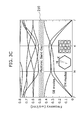
- the two-dimensional photonic crystal structure is a photonic crystal structure in which an arrangement pattern is arranged two-dimensionally as shown in FIGS. 3A and 3B (for more detail, refer to "Photonic Crystals: modeling the flow of light", John D. Joannopulos, et al., Princeton University Press, ISBN0-691-03744-2).
- waves having a normalized frequency ⁇ a/2 ⁇ C, where ⁇ is an angular frequency and C is a light speed
- This frequency band is herein called a photonic band gap 210.
- the photonic band gap 210 of the photonic crystal structure 110 between the transmission antenna 101 and the receiving antenna 102 is formed to have the same frequency band as a frequency band of waves to be transmitted and received.
- the frequency band which is blocked by the photonic crystal structure 110 includes a frequency band of waves which are transmitted or received by the receiving antenna 101 and the transmission antenna 102.
- wave leakage can be prevented in all directions between the transmission antenna 101 and the receiving antenna 102.
- the antenna device according to the first embodiment can achieve good isolation between the transmission antenna and the receiving antenna.
- the photonic band gap 210 exists near a frequency f determined by the following equation (1).
- c represents a light speed
- n eq represents an equivalent refractive index
- r represents a radius of the throughhole 205
- a represents an arrangement space of the throughhole 205
- no represents a refractive index of the throughhole 205 (air in the first embodiment)
- n 1 represents a refractive index of the substrate 205.
- the frequency band of the photonic band gap 210 varies depending on a difference of refractive indexes between substances of the photonic crystal structure.
- the photonic crystal structure 110 is formed by forming a plurality of throughholes between the transmission antenna 101 and the receiving antenna 102.
- the photonic crystal structure 110 has the photonic band gap 210 including a frequency of waves used by the transmission antenna 101 and the receiving antenna 102.
- the antenna device according to the first embodiment can prevent wave leakage between the transmission antenna 101 and the receiving antenna 102.
- the antenna device according to the first embodiment can achieve good isolation between the transmission antenna and the receiving antenna.
- the present invention is not limited to this embodiment.
- each of the elements (throughholes 105) of the photonic crystal structure 110 has been described to have a circular shape, but each throughhole 105 may be formed to have a polygonal shape or an ellipse shape.
- the throughholes 105 are arranged in a lattice pattern on the dielectric substrate 103 thereby realizing the photonic crystal structure 110, but, on the other hand, the photonic crystal structure may be realized by leaving parts of the dielectric substrate 103 in a lattice pattern.
- the photonic crystal structure 110 has been described to be a two-dimensional photonic crystal structure, but the photonic crystal structure 110 may be a three-dimensional photonic crystal structure.
- each of the transmission antenna 101 and the receiving antenna 102 has been described to be a planar microstrip patch antenna, but these antennas may be any antennas having other structures. Furthermore, each of the transmission antenna 101 and the receiving antenna 102 may have an array antenna structure. Still further, although the feeding scheme for the transmission antenna 101 and the receiving antenna 102 has been described to be the coplanar feeding scheme, the scheme may be any other schemes such a slot feeding scheme.
- the substrate 103 has been described to be a substrate made of dielectric substance, but the substrate 103 may be a substrate made of other substances, such as an alumina substrate or a ceramic substrate. Furthermore, although the substrate 103 has been described to be a monolayer substrate, the substrate 103 may be a multilayer substrate.
- the arrangement of the throughholes 105 has described to be an lattice pattern, but the arrangement may be any other arrangement.
- the antenna device has been described to have two elements of the transmission antenna 101 and the receiving antenna 102, but the antenna device may have two or more antenna elements. Moreover, the antenna device may have only one antenna element. If the antenna device has only one antenna device, the photonic crystal structure surrounds the antenna element to prevent unnecessary leakage from the antenna element. Here, by surrounding the antenna element by the photonic crystal structure, it is also possible to prevent noise into the antenna element. Even if the antenna device has two or more antenna elements, the photonic crystal structure can surround the antenna elements.
- the throughholes 105 have been described to pierce the substrate 103 and the ground conductor 104, but it is also possible that the throughholes 105 pierce only the substrate 103 and the ground conductor 104 does not have any holes.
- a photonic crystal structure is realized by filling each of the plurality of throughholes 105 of FIGS. 2A and 2B with a substance different from the substance of the substrate 103.
- FIG. 4A is a perspective view showing a structure of the antenna device according to the second embodiment.
- FIG. 4B is a cross sectional view taken along line A2 - B2 of FIG. 4A .
- the same reference numerals of FIGS. 2A and 2B are assigned to identical elements of FIGS. 4A and 4B , so that the detailed explanation for the identical elements is not given again below.
- the antenna device according to the second embodiment includes a photonic crystal structure 310 having a plurality of throughholes 306.
- the plurality of throughholes 306 are formed between the transmission antenna 101 and the receiving antenna 102.
- Each of the plurality of throughholes 306 is filled with a filling of a substance different from the substance of the substrate 103.
- the photonic crystal structure 310 is made of the substance of the substrate 103 and a substance different from the substance of the substrate 103.
- the substance of the fillings used for the throughholes 306 has a refraction index (relative permittivity) greater than a refraction index (relative permittivity) of the substance of the substrate 103.
- the fillings used for the throughholes 306 are made of silicon resin or the like.
- the antenna device in the antenna device according to the second embodiment, even if the space a for arranging the throughholes 306 is shorter than the space a of the antenna device according to the first embodiment, it is possible to form the photonic band gap 210 having the same frequency band as the first embodiment. As a result, it is possible to reduce a size of the photonic crystal structure 310.
- the antenna device by increasing a difference of refraction indexes between substances of the photonic crystal structure 310, it is possible to form the photonic crystal structure 310 having the photonic band gap 210 of a wide frequency band. As a result, the antenna device using a wide frequency range can improve isolation between the transmission antenna and the receiving antenna.
- the substance of the fillings for the throughholes 306 may be a wave absorber which can absorb waves.
- the substance of the wave absorber for the throughholes 306 is a substance which converts waves into heat using a carbon resistance loss, a magnetism loss of ferrite or the like.
- the same effects can be achieved, when a substance having a dielectric loss tangent greater than a dielectric loss tangent of dielectric substance which is a substance of the substrate 103 is used as the fillings for the throughholes 306.
- the throughholes 305 are arranged in a lattice pattern on the dielectric substrate 103 and then filled with the fillings to form the photonic crystal structure, but, on the other hand, the photonic crystal structure may be formed by leaving parts of the dielectric substrate 103 in a lattice pattern and a part except the parts of the dielectric substance 103 are filled with the fillings.
- the antenna device according to the third embodiment can achieve high isolation between the transmission antenna and the receiving antenna, by further including a ground conductor formed on a surface of the substrate 103 in the antenna device according to the second embodiment.
- FIG. 5A is a perspective view showing a structure of the antenna device according to the third embodiment.
- FIG. 5B is a cross sectional view taken along line A3 - B3 of FIG. 5A .
- the same reference numerals of FIGS. 4A and 4B are assigned to identical elements of FIGS. 5A and 5B , so that the detailed explanation for the identical elements is not given again below.
- the antenna device shown in FIGS. 5A and 5B differs from the antenna device according to the second embodiment in including the a top surface conductor 407 and a connection conductor 408.
- the top surface conductor 407 is formed on a surface of the substrate 103 between the transmission antenna 101 and the receiving antenna 102.
- connection conductor 408 is formed on an entire internal surface of each of the throughholes 306. After forming the throughholes, the inside of each of the throughholes 306 is plated, thereby forming the connection conductor 408. Then, after forming the connection conductor 408, each of the throughholes 306 is filled with a filling. The connection conductor 408 is contact to the ground conductor 104 and the top surface conductor 407. Therefore, the ground conductor 104, the top surface conductor 407, and the connection conductor 408 are electrically connected to ground.
- the top surface conductor 407 has holes with the same shape of the throughholes 306 formed on the substrate 103. This means that a part of the substrate 103, a part of the ground conductor 104, and a part of the top surface conductor 407 form a photonic crystal structure 410.
- the antenna device can improve isolation between the transmission antenna 101 and the receiving antenna 102, by forming the top surface conductor 407 on a top surface of the substrate 103 and the connection conductor 408 inside of each of the throughholes 306.
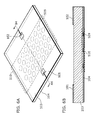
- the photonic crystal structure 410 is formed in all of the throughholes 306, the ground conductors 104, and the top surface conductor 407, but the third embodiment is not limited to the above.
- FIG. 6A is a perspective view of an antenna device in which a photonic crystal structure 510 is formed only in the ground conductor 104.
- FIG. 6B is a cross sectional view taken along line A4 - B4 of FIG. 6A .
- the photonic crystal structure 510 may be realized by forming circular holes 509 only in the ground conductor 104.
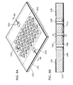
- FIG. 7A is a perspective view of an antenna device in which a photonic crystal structure 610 is formed only in a conductor 104 formed on a surface of the substrate 103.
- FIG. 7B is a cross sectional view taken along line A5 - B5 of FIG. 7A .
- the photonic crystal structure 610 may be realized by forming circular holes 609 only in the top surface conductor 407.
- the ground conductor 104 has a photonic crystal structure which has an arrangement pattern different from the arrangement pattern of the photonic crystal structure formed on the substrate 103.
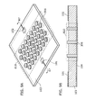
- FIG. 8A is a perspective view showing a structure of the antenna device according to the fourth embodiment.
- FIG. 8B is a cross sectional view taken along line A6 - B6 of FIG. 8A .
- the same reference numerals of FIGS. 2A and 2B are assigned to identical elements of FIGS. 8A and 8B , so that the detailed explanation for the identical elements is not given again below.
- a radius r1 of each of the plurality of throughholes 105 is different from a radius r2 of each of a plurality of holes 709 which are formed in the ground conductor 104.
- a photonic crystal structure 720 having an arrangement pattern different from a arrangement pattern of a photonic crystal structure 710 formed on the substrate 103 is formed.
- the arrangement pattern of the photonic crystal structure is determined by an arrangement space a, a radius, a shape (circular or polygonal, for example), and the like of the throughhole 105.
- the antenna device according to the fourth embodiment by forming the throughhole 105 and the hole 709 to have different arrangement patterns, a frequency band of the photonic band gaps 210 of each of the photonic crystal structure 710 and the photonic crystal structure 720 is adjusted to the frequency band of waves used by the antenna device. As a result, the antenna device according to the fourth embodiment can improve isolation between the transmission antenna and the receiving antenna.
- the radius r2 of the hole 709 is longer than the radius r1 of the throughhole 105, but the radius r2 of the hole 709 may be shorter than the radius r1 of the throughhole 105.
- it has been described to form the throughhole 105 and the hole 709 to have different radius it is also possible to form the throughhole 105 and the hole 709 to have different arrangement space a, without making a difference in the radius. Still further, it is also possible to form the throughhole 105 and the hole 709 to have different radius and also different arrangement space a.
- shapes of both of the throughhole 105 and the hole 709 are the same, but the shape may be different between the throughhole 105 and the hole 709.
- one of the throughhole 105 and the hole 709 may have an ellipse shape or a polygonal shape.
- the conductor 407 is formed on the surface of the substrate 103 as shown in FIGS. 5A and 5B , it is possible to form, in the top surface conductor 407, a photonic crystal structure having an arrangement pattern different from the arrangement pattern of the photonic crystal structure formed on the substrate 103. Further, arrangement patterns of the photonic crystal structures formed in the top surface conductor 407, the substrate 103, and the ground conductor 104 may be different from one another.
- each of the fillings in the throughholes forming the photonic crystal structure protrudes from a surface of the substrate.
- FIG. 9A is a perspective view showing a structure of the antenna device according to the fifth embodiment.
- FIG. 9B is a cross sectional view taken along line A7 - B7 of FIG. 9A .
- the same reference numerals of FIGS. 4A and 4B are assigned to identical elements of FIG. 9A and 9B , so that the detailed explanation for the identical elements is not given again below.
- the antenna device according to the fifth embodiment differs from the antenna device according to the second embodiment in that each of fillings with which each of the throughholes 306 is filled protrudes from a surface of the substrate 103.
- the antenna device according to the fifth embodiment can block waves leaked above the surface of the substrate.
- the antenna device can improve isolation between the transmission antenna and the receiving antenna, by removing a part of the ground conductor 104 between the transmission antenna and the receiving antenna.
- FIG. 10A is a perspective view showing a structure of the antenna device according to the sixth embodiment.
- FIG. 10B is a cross sectional view taken along line A8 - B8 of FIG. 10A .
- the same reference numerals of FIGS. 2A and 2B are assigned to identical elements of FIGS. 10A and 10B , so that the detailed explanation for the identical elements is not given again below.
- the antenna device according to the sixth embodiment differs from the antenna device according to the first embodiment in that a part of the ground conductor between the transmission antenna 101 and the receiving antenna 102 is removed.
- the antenna device according to the sixth embodiment includes ground conductors 104a and 104b, instead of the ground conductor 104 which is formed on an entire rear surface of the substrate 103 in the first to fifth embodiments.
- the ground conductor 104 of the sixth embodiment has a gap between the transmission antenna 101 and the receiving antenna 102.
- the ground conductor 104a and the ground conductor 104b are arranged with a gap being positioned therebetween.
- the ground conductor 104a is formed on a region of a rear surface of the substrate 103.
- the transmission antenna 101 is formed on a region corresponding to the above region.
- the ground conductor 104b is formed on another region of the rear surface of the substrate 103.
- the receiving antenna 102 is formed on a region corresponding to the above region.
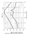
- FIG. 11 is a graph plotting a propagation amount of the waves leaked between the transmission antenna and the receiving antenna versus a frequency of waves used by the antenna device.
- a waveform 1001 shown in FIG. 11 represents a propagation amount of waves between the transmission antenna and the receiving antenna, in the case where, in FIGS 10A and 10B , a relative permittivity of the substrate 103 is 3.02, a radius r of the throughhole 105 is 1.8 mm, an arrangement space a of the throughhole 105 is 4.5 mm, a space between the transmission antenna 101 and the receiving antenna 102 is 30 mm, an isolation region of each of the ground conductors 104a and 104b is 20 mm, and a size of each patch antenna element in the transmission antenna 101 and the receiving antenna 102 is 3.1-mm-square.
- a waveform 1002 shown in FIG. 11 represents a propagation amount of waves between the transmission antenna and the receiving antenna, in the conventional case where the photonic crystal structure is not formed and the ground conductor 104 is arranged on an entire rear surface of the substrate 103.
- an amount of propagation waves having the waveform 1001 becomes smaller by about 30 dB, in comparison with the waveform 1002,.
- an amount of propagation waves having the waveform 1001 becomes smaller by about 17 dB on an average, in comparison with the waveform 1002.
- the antenna device can achieve very good isolation between the transmission antenna and the receiving antenna. Furthermore, if the ground conductor is separated into plural ground conductors set apart from each other without forming the photonic crystal structure (not shown), it is possible to reduce the propagated waves between the transmission antenna and the receiving antenna by about 10 dB. Still further, in the case of the antenna device in which the photonic crystal structure 110 is formed without the separation of the ground conductor 104 as shown in FIGS. 2A and 2B , it is possible to reduce the propagated waves between the transmission antenna and the receiving antenna by about 8 dB.
- the antenna device can improve the isolation between the transmission antenna and the receiving antenna, by separating the ground conductor 104 into plural ground conductors formed on a rear surface corresponding to the transmission antenna 101 and on a rear surface corresponding to the receiving antenna 102, respectively.
- FIGS. 10A and 10B it should be noted that a photonic crystal structure 901 is shown in FIGS. 10A and 10B , but it is possible to separate the ground conductor 104 into plural ground conductors set apart from each other without forming the photonic crystal structure 910.
- the antenna device can improve isolation between the transmission antenna and the receiving antenna, by embedding a wave absorber between the transmission antenna and the receiving antenna.
- FIG. 12A is a perspective view showing a structure of the antenna device according to the seventh embodiment.
- FIG. 12B is a cross sectional view taken along line A9 - B9 of FIG. 12A .
- the same reference numerals of FIGS. 2A and 2B are assigned to identical elements of FIGS. 12A and 12B , so that the detailed explanation for the identical elements is not given again below.
- a wave absorber 1110 is formed between the transmission antenna 101 and the receiving antenna 102.
- the wave absorber 1110 is embedded in a region where the photonic crystal structure 110 is formed in the first embodiment.
- the substance of the wave absorber 1110 converts waves into heat using a carbon resistance loss, a magnetism loss of ferrite or the like.
- the antenna device can improve isolation between the transmission antenna and the receiving antenna, since waves leaked between the transmission antenna and the receiving antenna are absorbed and then converted into heat by the wave absorber 1110.
- the ground conductor 104a formed on a rear side corresponding to the transmission antenna 101 and the ground conductor 104b formed on a rear side corresponding to the receiving antenna 102 are completely separated from each other.
- the ground conductors 104a and 104b may be connected via a line.
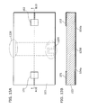
- FIG. 13A is a plane view of an antenna device in which ground conductors are connected to each other via a line.
- FIG. 13B is a cross sectional view taken along line A10 - B10 of FIG. 13A .
- a connection line which electrically connects the ground conductor 104a to the ground conductor 104b.
- a connection serpentine line which has serpentines, to connect the ground conductor 104a to the ground conductor 104b.
- the connection serpentine line 1230 By using the connection serpentine line 1230, a propagation distance of the leaked waves can be extended. In other words, by using the connection serpentine line 1230, the waves leaked between the transmission antenna and the receiving antenna through the connection line can be reduced more than the case of using the connection line 1220 which is a straight line.
- the present invention can be used as an antenna device, and more specifically as a high-efficiency wireless communication device or a radar device.
Landscapes
- Physics & Mathematics (AREA)
- Optics & Photonics (AREA)
- Details Of Aerials (AREA)
- Waveguide Aerials (AREA)
- Aerials With Secondary Devices (AREA)
Applications Claiming Priority (2)
| Application Number | Priority Date | Filing Date | Title |
|---|---|---|---|
| JP2005358219A JP2007166115A (ja) | 2005-12-12 | 2005-12-12 | アンテナ装置 |
| PCT/JP2006/315470 WO2007069367A1 (ja) | 2005-12-12 | 2006-08-04 | アンテナ装置 |
Publications (1)
| Publication Number | Publication Date |
|---|---|
| EP1962377A1 true EP1962377A1 (de) | 2008-08-27 |
Family
ID=38162683
Family Applications (1)
| Application Number | Title | Priority Date | Filing Date |
|---|---|---|---|
| EP06782328A Withdrawn EP1962377A1 (de) | 2005-12-12 | 2006-08-04 | Antenneneinrichtung |
Country Status (4)
| Country | Link |
|---|---|
| US (1) | US8081117B2 (de) |
| EP (1) | EP1962377A1 (de) |
| JP (1) | JP2007166115A (de) |
| WO (1) | WO2007069367A1 (de) |
Cited By (4)
| Publication number | Priority date | Publication date | Assignee | Title |
|---|---|---|---|---|
| WO2014009069A3 (de) * | 2012-07-10 | 2014-03-20 | Endress+Hauser Gmbh+Co. Kg | Leiterplatte mit einer störwellen aussendenden hochfrequenzbaugruppe |
| EP2551956A4 (de) * | 2010-03-23 | 2014-12-03 | Furukawa Electric Co Ltd | Antenne und integrierte antenne |
| EP2790270A4 (de) * | 2011-12-08 | 2015-07-29 | Denki Kogyo Co Ltd | Sende-/empfangsgetrennte antenne mit gemeinsamer polarisation |
| WO2018111394A1 (en) * | 2016-12-14 | 2018-06-21 | Raytheon Company | Isolation barrier |
Families Citing this family (42)
| Publication number | Priority date | Publication date | Assignee | Title |
|---|---|---|---|---|
| US9666933B2 (en) * | 2005-03-09 | 2017-05-30 | Xirrus, Inc. | Wireless local area network antenna array |
| JP4650302B2 (ja) * | 2006-03-07 | 2011-03-16 | 三菱電機株式会社 | アレーアンテナ |
| JP5019033B2 (ja) * | 2007-03-16 | 2012-09-05 | 日本電気株式会社 | コモンモード電流抑制ebgフィルタ |
| JP5012407B2 (ja) * | 2007-10-22 | 2012-08-29 | 日本電気株式会社 | Ebg材料を用いたコモンモード電流抑制フィルタ |
| JP4527760B2 (ja) * | 2007-10-26 | 2010-08-18 | 三菱電機株式会社 | アンテナ装置 |
| JP5112204B2 (ja) * | 2008-07-15 | 2013-01-09 | 原田工業株式会社 | アンテナエレメント間の相互結合を抑制可能なアンテナ装置 |
| US7773033B2 (en) * | 2008-09-30 | 2010-08-10 | Raytheon Company | Multilayer metamaterial isolator |
| JP5414451B2 (ja) * | 2009-10-21 | 2014-02-12 | パナソニック株式会社 | アンテナ装置 |
| EP2533362B1 (de) * | 2010-02-05 | 2017-08-16 | Mitsubishi Electric Corporation | Mikrostreifenantenne und radarmodul |
| JP5638827B2 (ja) * | 2010-04-02 | 2014-12-10 | 古河電気工業株式会社 | 内蔵型レーダ用送受一体アンテナ |
| US8659480B2 (en) * | 2010-05-05 | 2014-02-25 | The Boeing Company | Apparatus and associated method for providing a frequency configurable antenna employing a photonic crystal |
| CN102227039A (zh) * | 2011-04-17 | 2011-10-26 | 江苏大学 | 一种交叉异质排列光子晶体天线 |
| JP6281868B2 (ja) * | 2013-03-08 | 2018-02-21 | 国立大学法人大阪大学 | フォトニック結晶スラブ電磁波吸収体および高周波金属配線回路、電子部品、および送信器、受信器および近接無線通信システム |
| JP6095444B2 (ja) * | 2013-03-29 | 2017-03-15 | 富士通テン株式会社 | アンテナ装置およびレーダ装置 |
| EP3063832B1 (de) * | 2013-10-29 | 2022-07-06 | Zoll Medical Israel Ltd. | Antennensysteme und vorrichtungen sowie verfahren zur herstellung davon |
| US11013420B2 (en) | 2014-02-05 | 2021-05-25 | Zoll Medical Israel Ltd. | Systems, apparatuses and methods for determining blood pressure |
| US9891266B2 (en) | 2014-02-25 | 2018-02-13 | Taiwan Semiconductor Manufacturing Co., Ltd. | Test circuit and method |
| WO2016040337A1 (en) | 2014-09-08 | 2016-03-17 | KYMA Medical Technologies, Inc. | Monitoring and diagnostics systems and methods |
| US9960485B2 (en) * | 2014-11-19 | 2018-05-01 | Panasonic Intellectual Property Management Co., Ltd. | Antenna device using EBG structure, wireless communication device, and radar device |
| US10548485B2 (en) | 2015-01-12 | 2020-02-04 | Zoll Medical Israel Ltd. | Systems, apparatuses and methods for radio frequency-based attachment sensing |
| JP6512402B2 (ja) * | 2015-05-20 | 2019-05-15 | パナソニックIpマネジメント株式会社 | アンテナ装置、無線通信装置、及びレーダ装置 |
| US10422870B2 (en) | 2015-06-15 | 2019-09-24 | Humatics Corporation | High precision time of flight measurement system for industrial automation |
| US10591592B2 (en) | 2015-06-15 | 2020-03-17 | Humatics Corporation | High-precision time of flight measurement systems |
| AU2016371057A1 (en) | 2015-12-17 | 2018-07-19 | Humatics Corporation | Radio-frequency localization techniques and associated systems, devices, and methods |
| US10811784B2 (en) * | 2016-03-01 | 2020-10-20 | Kymeta Corporation | Broadband RF radial waveguide feed with integrated glass transition |
| CN107706529B (zh) * | 2016-08-08 | 2021-01-15 | 华为技术有限公司 | 一种去耦组件、多天线系统及终端 |
| US10505255B2 (en) * | 2017-01-30 | 2019-12-10 | Infineon Technologies Ag | Radio frequency device packages and methods of formation thereof |
| CN106953173B (zh) * | 2017-02-23 | 2020-04-28 | 上海华为技术有限公司 | 一种双极化天线隔离装置及方法 |
| JP7057517B2 (ja) | 2017-06-23 | 2022-04-20 | 株式会社ソシオネクスト | アンテナ装置 |
| EP3664694B1 (de) | 2017-08-10 | 2025-12-10 | ZOLL Medical Israel Ltd. | System zur physiologischen überwachung von patienten |
| JP7019366B2 (ja) * | 2017-10-04 | 2022-02-15 | 株式会社ヨコオ | アンテナ装置 |
| JP7244243B2 (ja) * | 2018-09-28 | 2023-03-22 | 株式会社デンソーテン | アンテナ装置 |
| CN112970146B (zh) * | 2018-10-31 | 2024-05-24 | 株式会社村田制作所 | 布线基板、天线模块和通信装置 |
| EP3926756A4 (de) * | 2019-02-13 | 2022-11-09 | The University of Tokyo | Schaltungssubstrat, antennenelement, millimeterwellenabsorber zum einbau in ein substrat und verfahren zur rauschverminderung in einem schaltungssubstrat |
| EP3700005A1 (de) * | 2019-02-25 | 2020-08-26 | Nokia Solutions and Networks Oy | Senden und/oder empfangen von hochfrequenzsignalen |
| EP3918664B1 (de) | 2019-03-14 | 2023-10-11 | Huawei Technologies Co., Ltd. | Umlenkstruktur für elektromagnetische wellen |
| US11467468B2 (en) * | 2019-05-28 | 2022-10-11 | The Board Of Trustees Of The Leland Stanford Junior University | Dispersion engineered phased array |
| DE102019214124A1 (de) * | 2019-09-17 | 2021-03-18 | Continental Automotive Gmbh | Antennenvorrichtung und Fahrzeug aufweisend eine Antennenvorrichtung |
| US11784416B2 (en) * | 2020-01-06 | 2023-10-10 | Raytheon Company | Tunable radio frequency (RF) absorber and thermal heat spreader |
| CN111817000B (zh) * | 2020-07-07 | 2023-06-16 | 西安朗普达通信科技有限公司 | 一种采用散热孔结构改善多天线系统的耦合性能的方法 |
| US12080415B2 (en) | 2020-10-09 | 2024-09-03 | Humatics Corporation | Radio-frequency systems and methods for co-localization of medical devices and patients |
| US11924963B2 (en) | 2022-02-03 | 2024-03-05 | Raytheon Company | Printed-circuit isolation barrier for co-site interference mitigation |
Family Cites Families (22)
| Publication number | Priority date | Publication date | Assignee | Title |
|---|---|---|---|---|
| JPH04140905A (ja) | 1990-10-01 | 1992-05-14 | Hitachi Chem Co Ltd | 平面アンテナ |
| JP3115032B2 (ja) | 1991-07-06 | 2000-12-04 | コニカ株式会社 | トナー |
| JPH0511501U (ja) * | 1991-07-19 | 1993-02-12 | 三菱電機株式会社 | マイクロ波回路 |
| JPH10200326A (ja) | 1997-01-07 | 1998-07-31 | Mitsubishi Electric Corp | アンテナ装置 |
| US20030186725A1 (en) | 1997-03-18 | 2003-10-02 | Matsushita Electric Industrial Co., Ltd. | Calibration apparatus for array antenna radio receiving apparatus |
| US5923225A (en) * | 1997-10-03 | 1999-07-13 | De Los Santos; Hector J. | Noise-reduction systems and methods using photonic bandgap crystals |
| US6262495B1 (en) | 1998-03-30 | 2001-07-17 | The Regents Of The University Of California | Circuit and method for eliminating surface currents on metals |
| US6597851B2 (en) * | 2000-08-09 | 2003-07-22 | Massachusetts Institute Of Technology | Periodic dielectric structure having a complete three-dimensional photonic band gap |
| JP4702870B2 (ja) * | 2001-07-27 | 2011-06-15 | 独立行政法人理化学研究所 | 3次元フォトニック結晶およびその製造方法ならびにプローブ |
| JP2003078337A (ja) | 2001-08-30 | 2003-03-14 | Tokai Univ | 積層アンテナ |
| JP2003289215A (ja) | 2002-03-28 | 2003-10-10 | Murata Mfg Co Ltd | アンテナの配置構成およびアンテナモジュールおよび通信機 |
| JP3821039B2 (ja) * | 2002-04-09 | 2006-09-13 | 株式会社デンソー | アンテナ装置 |
| US6954177B2 (en) | 2002-11-07 | 2005-10-11 | M/A-Com, Inc. | Microstrip antenna array with periodic filters for enhanced performance |
| US7432775B2 (en) * | 2003-03-05 | 2008-10-07 | Banpil Photonics, Inc. | High speed electronics interconnect having a dielectric system with cylindrical holes therein |
| JP2005094440A (ja) | 2003-09-18 | 2005-04-07 | Tdk Corp | アンテナ装置およびレーダ装置 |
| US7145518B2 (en) | 2003-09-30 | 2006-12-05 | Denso Corporation | Multiple-frequency common antenna |
| JP2005124056A (ja) | 2003-10-20 | 2005-05-12 | Alps Electric Co Ltd | パッチアンテナ |
| JP4418250B2 (ja) * | 2004-02-05 | 2010-02-17 | 株式会社ルネサステクノロジ | 高周波回路モジュール |
| JP3784807B2 (ja) * | 2004-02-24 | 2006-06-14 | 株式会社エヌ・ティ・ティ・ドコモ | マイクロストリップアンテナ |
| WO2005083902A1 (en) | 2004-02-27 | 2005-09-09 | Matsushita Electric Industrial Co., Ltd. | Method and apparatus for transmitting data in a multi-antenna wireless system |
| JP4140905B2 (ja) | 2004-03-22 | 2008-08-27 | インターナショナル・ビジネス・マシーンズ・コーポレーション | 記憶装置及びプログラム |
| JP4843611B2 (ja) * | 2004-10-01 | 2011-12-21 | デ,ロシェモント,エル.,ピエール | セラミックアンテナモジュール及びその製造方法 |
-
2005
- 2005-12-12 JP JP2005358219A patent/JP2007166115A/ja active Pending
-
2006
- 2006-08-04 US US12/092,741 patent/US8081117B2/en not_active Expired - Fee Related
- 2006-08-04 WO PCT/JP2006/315470 patent/WO2007069367A1/ja not_active Ceased
- 2006-08-04 EP EP06782328A patent/EP1962377A1/de not_active Withdrawn
Non-Patent Citations (1)
| Title |
|---|
| See references of WO2007069367A1 * |
Cited By (10)
| Publication number | Priority date | Publication date | Assignee | Title |
|---|---|---|---|---|
| EP2551956A4 (de) * | 2010-03-23 | 2014-12-03 | Furukawa Electric Co Ltd | Antenne und integrierte antenne |
| US9070967B2 (en) | 2010-03-23 | 2015-06-30 | Furukawa Electric Co., Ltd. | Antenna and combination antenna |
| EP2790270A4 (de) * | 2011-12-08 | 2015-07-29 | Denki Kogyo Co Ltd | Sende-/empfangsgetrennte antenne mit gemeinsamer polarisation |
| US9379434B2 (en) | 2011-12-08 | 2016-06-28 | Denki Kogyo Co., Ltd. | Transmitting-receiving-separated dual-polarization antenna |
| WO2014009069A3 (de) * | 2012-07-10 | 2014-03-20 | Endress+Hauser Gmbh+Co. Kg | Leiterplatte mit einer störwellen aussendenden hochfrequenzbaugruppe |
| CN104488365A (zh) * | 2012-07-10 | 2015-04-01 | 恩德莱斯和豪瑟尔两合公司 | 装备有发射干扰波的高频部件的电路板 |
| US9801268B2 (en) | 2012-07-10 | 2017-10-24 | Endress + Hauser Gmbh + Co. Kg | Circuit board equipped with a high-frequency component emitting interference waves |
| CN104488365B (zh) * | 2012-07-10 | 2018-07-17 | 恩德莱斯和豪瑟尔两合公司 | 装备有发射干扰波的高频部件的电路板 |
| WO2018111394A1 (en) * | 2016-12-14 | 2018-06-21 | Raytheon Company | Isolation barrier |
| US10454180B2 (en) | 2016-12-14 | 2019-10-22 | Raytheon Company | Isolation barrier |
Also Published As
| Publication number | Publication date |
|---|---|
| JP2007166115A (ja) | 2007-06-28 |
| US20090153433A1 (en) | 2009-06-18 |
| US8081117B2 (en) | 2011-12-20 |
| WO2007069367A1 (ja) | 2007-06-21 |
Similar Documents
| Publication | Publication Date | Title |
|---|---|---|
| EP1962377A1 (de) | Antenneneinrichtung | |
| CN115280181B (zh) | 具有低纹波辐射方向图的天线装置 | |
| EP2146556B1 (de) | Wellenleiterstruktur und Leiterplatte | |
| EP0883328B1 (de) | Leiterplatte mit einer Übertragungsleitung für hohe Frequenzen | |
| US9184505B2 (en) | Dielectric cavity antenna | |
| KR101761920B1 (ko) | 유전체 도파관 안테나 | |
| KR101492714B1 (ko) | 마이크로스트립 라인 및 도파관 결합용 어댑터 | |
| CN105470611B (zh) | 高频电力转换机构 | |
| US9705174B2 (en) | Dielectric waveguide having a core and cladding formed in a flexible multi-layer substrate | |
| JP2004516734A (ja) | アンテナ装置 | |
| KR102536245B1 (ko) | 레이돔, 차량용 레이더 센서 및 이를 포함하는 차량용 감지 장치 | |
| CN113394560B (zh) | 天线组件、天线装置以及可移动平台 | |
| US12603439B2 (en) | Waveguides and waveguide sensors with signal-improving grooves and/or slots | |
| CN114039212A (zh) | 一种低通宽阻的透波结构 | |
| US11011814B2 (en) | Coupling comprising a conductive wire embedded in a post-wall waveguide and extending into a hollow tube waveguide | |
| EP1432064A1 (de) | HF Modul und Methode zur Anordnung von Durchgangslöchern in einem HF Modul | |
| JPWO2019139003A1 (ja) | フィルタ | |
| JPH10107518A (ja) | 誘電体導波管線路および配線基板 | |
| KR102059329B1 (ko) | 초광대역 다이폴 안테나 | |
| JP5242362B2 (ja) | アンテナ装置 | |
| TWI738119B (zh) | 天線模組 | |
| JPH04140905A (ja) | 平面アンテナ | |
| KR20150008765A (ko) | 레이더 장치 | |
| JPH11136009A (ja) | 高周波用フレキシブル線路 | |
| JPH07191129A (ja) | 送受信アンテナ分離型レーダー装置 |
Legal Events
| Date | Code | Title | Description |
|---|---|---|---|
| PUAI | Public reference made under article 153(3) epc to a published international application that has entered the european phase |
Free format text: ORIGINAL CODE: 0009012 |
|
| RAP1 | Party data changed (applicant data changed or rights of an application transferred) |
Owner name: PANASONIC CORPORATION |
|
| STAA | Information on the status of an ep patent application or granted ep patent |
Free format text: STATUS: THE APPLICATION IS DEEMED TO BE WITHDRAWN |
|
| 18D | Application deemed to be withdrawn |
Effective date: 20080714 |